
Recommended
Recommended
More Related Content
What's hot
What's hot (19)
Similar to Pwbs331 reliable RS485 network solution
Similar to Pwbs331 reliable RS485 network solution (20)
Recently uploaded
Recently uploaded (20)
Pwbs331 reliable RS485 network solution
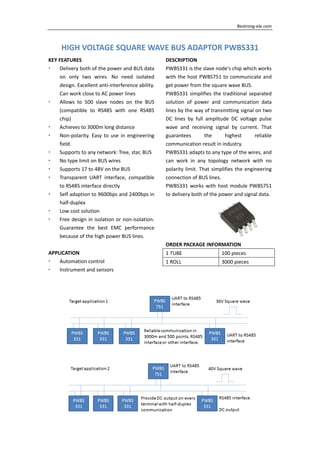
- 1. Bestrong‐ele.com HIGH VOLTAGE SQUARE WAVE BUS ADAPTOR PWBS331 KEY FEATURES Delivery both of the power and BUS data on only two wires. No need isolated design. Excellent anti‐interference ability. Can work close to AC power lines Allows to 500 slave nodes on the BUS (compatible to RS485 with one RS485 chip) Achieves to 3000m long distance Non‐polarity. Easy to use in engineering field. Supports to any network: Tree, star, BUS No type limit on BUS wires Supports 17 to 48V on the BUS Transparent UART interface, compatible to RS485 interface directly Self adaption to 9600bps and 2400bps in half‐duplex Low cost solution Free design in isolation or non‐isolation. Guarantee the best EMC performance because of the high power BUS lines. APPLICATION Automation control Instrument and sensors DESCRIPTION PWBS331 is the slave node's chip which works with the host PWBS751 to communicate and get power from the square wave BUS. PWBS331 simplifies the traditional separated solution of power and communication data lines by the way of transmitting signal on two DC lines by full amplitude DC voltage pulse wave and receiving signal by current. That guarantees the highest reliable communication result in industry. PWBS331 adapts to any type of the wires, and can work in any topology network with no polarity limit. That simplifies the engineering connection of BUS lines. PWBS331 works with host module PWBS751 to delivery both of the power and signal data. ORDER PACKAGE INFORMATION 1 TUBE 100 pieces 1 ROLL 3000 pieces
- 2. Bestrong‐ele.com ABSOLUTE MAXIMUM RATINGS(1) Table1. PARAMETER RANGE Vcc to Ground (GNG) ‐0.3V~6.0V TX, RX, PI, PO ‐0.3V~Vcc+0.3V Storage temperature ‐65 to +150℃ Operating temperature ‐40℃ to +85℃ Soldering temperature (10s) 220℃ ESD (HBM) 4KV ESD (CDM) 2KV ESD (MM) 400V (1) Stresses beyond those listed under "Absolute Maximum Ratings" may cause permanent damage to the device. Working on the absolute maximum rating in long time will cause unstable performance PIN NAME Fig.1 ESD warning ESD (Electrostatic discharge) protection notice Circuit board and the components on the board may have static with high power. Discharging may cause damage on the device. ESD protection is important to ensure the best performance of the device. Table2. PIN DESCRIPTION PIN NUMBER PIN NAME FUNCTION 1 VCC Power supply 2 TX Data transmitter 3 RX Data receiver 4 NC No connection 5 PO Square wave BUS signal output 6 PI Square wave BUS signal input 7 NC No connection 8 GND Ground
- 3. Bestrong‐ele.com GENERAL ELECTRICAL CHARACTERISTICS All voltage referenced to GND, unless otherwise noted Table3. PARAMETER CONDITIONS MIN TYPE MAX UNIT DC electrical characteristics VCC power supply input Test on Vcc 2.7 5.5 V ICC quiescent current Vcc=3.3V, no data communicate 0.8 mA Vcc=5V, no data communicate 1.2 mA UART electrical characteristics VIL RX low level voltage 2.7<Vcc<5.5V 0.2Vcc V VIH RX high level voltage 2.7<Vcc<5.5V 0.6Vcc V VOL TX low level voltage ITX=1.1mA 0.6 V VOH TX high level voltage ITX=1.1mA Vcc‐0.7 V UART timer characteristics TON power on delay (1) 2 20 mS Tbit communication time for 1bit 9600bps 100 104 108 uS 2400bps 410 416 428 uS Td(TX) transmitting delay (2) 11*Tbit uS Td(RX) receiving delay (2) 11*Tbit uS (1) The delay time from power on to the device working well (2) The delay time caused by data buffer. No more extra delay time after the device transmitting or receiving in continues UART INTERFACE PWBS331 detects and adapts the data rate of 9600bps or 2400bps automatically. Transmit and receive 8bits or 9bits automatically. The 9th bit can be used as data, check or address 8bits mode: start + 8bits data + stop 9bits mode: start + 8bits data + 9th data+ stop
- 4. Bestrong‐ele.com APPLICATION GUIDE Target power got from square wave BUS DC output can be got from the DCS terminal on fig.6. This terminal deliveries rectified DC power which comes from square wave BUS and host side. This terminal can also be used directly as a DC output or use DC/DC (LDO) to have a target fixed output. Notice: The target load can’t be connected to the square wave BUS lines directly. That may cause a protection action by host side. Target load Square wave BUS provides high power DC output to slave nodes. Target load can be any style: resistance, capacitive, inductive load from motor, electric actuator, electric relay, high power LED and so on. Fluctuant current on the load won't influence the communication ability on square wave BUS. Vcc on PWBS331 Vcc on PWBS331 can be large range to adapt any LDO or DC/DC converter. Vcc also can share from the power of MCU. It can be got from rectified square wave BUS or local battery of other way. FUSE and protection circuit on slave site The fuse on fig.6 can be PPTC (Polyer Positive Temperature Coefficent) or resistance, which can avoid the circuit short and surging caused by power on. Fuse can help to make the damaged slave node break away from BUS system, and then host side can detect the fault on slave site. Fuse is not essential. Pure load in system If there are pure loads in slave nodes of the system, fig.5 a simple circuit can be used to down the total cost.
- 5. Bestrong‐ele.com Note: BRIDGE: MB6S or 1N4007 (M7). BRIDGE can't use schottky bridge rectifier in here. D1: US1M or RS1M. Here must be fast recovery diode R1, R2: Do not change value on these two parts. CX1 CX2: EMC capacitor, range from 30pF to 100pF C1 and the output wave on DCS terminal C1 is storage energy capacitor to make a stabilizing voltage output. C1 is selected by target current load. Voltage wave on the DCS terminal has no influence on the communication ability. The requirement on DCS terminal must be high than 10V. C1 can be electrolytic capacitor and tantalum capacitor or ceramic capacitor. It is the best to use 470uf or 1000uF Power level on the square wave BUS lines There must be at least 12V peak voltage on the BUS line's slave site to ensure PWBS331 working well. Please provide right DC input to host site to make sure the slave terminal of BUS can be high than 12V. APPLICATION CIRCUIT Isolated design and other power supply source If slave node needs power from other source such as local AC commercial power, please refer fig.7 circuit below. Compare with the isolated RS485 application, below circuit doesn't need isolated DC/DC power which can down the cost. Power on the op‐coupler side can be got from square wave BUS. Battery backup for slave node If adopts battery backup, please refer fig.8 which means the power source for slave node can be got from either of the BUS or battery