X-Ray Properties of NGC 253ʼs Starburst-driven Outflow
MERRY-MAF-WNF-PosterFinalFinal-1
1. GDOES Characterization of TaN as Cu Diffusion Barrier
Scott P. Merry1,2, Tianna Hankins1,2, Liam Bradshaw2, Fred Newman3, and Michael Khbeis3
1Nanotechnology Department, North Seattle College, Seattle, WA 98103
2Molecular Analysis Facility, University of Washington, Seattle, WA 98195
3Washington Nanofabrication Facility, University of Washington, Seattle, WA 98195
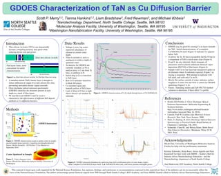
Data /Results
Figure 4. GDOES characterization of Cu by depth through layers of Cu/TaN/SiO2/Si.
• Voltage (y axis, log scale)
represents abundance of
element at current crater
depth.
• Time in seconds (x axis) is
analogous to relative depth of
sputtered crater.
• Ta detector for GDOES not
currently installed, so Ni is
used as proxy (<1 nm from Ta
line), in addition to N.
• Initial drop in Cu is transition
to TaN layer.
• Rise in O indicates transition
to thick SiO2 layer.
• Cu increases again just
beneath surface of SiO2 layer.
• Lack of drop in O line at right
shows haven’t yet reached Si
substrate.
Introduction
• Thru-silicon via holes (TSVs) can dramatically
increase computing memory and speed while
reducing device size and power.
• A tantalum nitride (TaN) barrier layer is thought to
reduce diffusion of copper (Cu) into silicon (Si), thus
preventing unwanted electric signal crosstalk.
• Glow discharge optical emission spectrometry
(GDOES) identifies the elements present at each
depth in a stack of film layers.
• We hypothesized GDOES could be used to
characterize the effectiveness of different TaN deposit
methods as Cu diffusion barriers.
Conclusions
• GDOES may be good for sensing Cu in layers beneath
the TaN. Initial characterization of a complete
Cu/TaN/SiO2/Si stack (Figure 4) indicates Cu appears
below TaN.
• As proxy for Ta, Ni line is acceptable but the N line as
a component of TaN is much more clear (Figure 4).
• H and C are also detected, likely remnants of
precursors used in plasma enhanced chemical vapor
deposition (PECVD) of film layers (Figure 4).
• Sample with Cu on top layer had unexpected spikes in
all elements where Si substrate expected (Figure 5 a).
Arcing is suspected. Will attempt to replicate with
full stack, and with only Cu on Si.
• Mostly flat surface outside of crater indicates surface
roughness at crater rim and floor is caused by GDOES
sputtering (Figure 5 b, d).
• Future: Annealing studies and TaN PECVD method
variation to determine if these affect Cu profile.
References
• Horiba GD-Profiler-2: Glow Discharge Optical
Emission Spectrometer. Molecular Engineering &
Sciences Institute,
http://www.moles.washington.edu/maf/research-
tools/gdoes/ (accessed May 16, 2016).
• Lamont, Paul W. Leading-edge Materials Science
Research. New York: Nova Science, 2008.
• Nelis, T.; Payling, R. Glow Discharge Optical Emission
Spectroscopy: a Practical Guide; Royal Society of
Chemistry: Cambridge, UK, 2003.
• Schneider, Claus M., and Wetzig Klaus. Metal Based
Thin Films for Electronics. Weinheim: Wiley-VCH,
2003. Print.
Acknowledgments
Micah Glaz, University of Washington Molecular Analysis
Facility for help with the profilometer instrument.
Kristine Schroeder, Brian Rucci, Alissa Agnello and Peter
Kazarinoff for their work with SHINE – Seattle’s Hub for
Industry-driven Nanotechnology Education – and the
Nanotechnology department at North Seattle College.
Ann Murkowski, RST Academy, North Seattle College.
Figures 5. GDOES elemental abundance by sputtering time (left); profilometer plots of crater shapes (right).
a, b: Complete Cu/TaN/SiO2/Si layer stack. c, d: TaN/SiO2/Si stack only, with lower pressure and higher power.
Methods
GDOES Instrument
a. b.
Figure 1. a. Ideal thru-silicon via hole. b. Flat thin films test setup.
Cu
TaN
SiO2
Si
Thin Film Test Setup
Thru-Silicon Via Hole
TaN
SiO2
SiCu
a.
b.
Figure 2. GDOES plasma ionizes argon to sputter crater in sample;
ejected sample atoms ionized; e- transition wavelengths detected.
Source: Horiba Scientific, GD Profiler 2 User Manual rev
September 2010.
Oxygen
Copper
Nickel (Tantalum Proxy)
c. d.
Crater Sputtered in Sample
Figure 3. Crater, diameter 4 mm.
Source: Micah Glaz, MolecularAnalysis Facility, University of
Washington.
-5000
-4000
-3000
-2000
-1000
0
1000
2000
3000
4000
5000
0 1 2 3 4 5 6 7
z-position (nm)
x-position (mm)
1
3
4
5
6
9
10 01
10 02
-4000
-3000
-2000
-1000
0
1000
2000
3000
4000
0 1 2 3 4 5 6 7 8z position (nm)
x position (mm)
Cu_TaN_01
Cu_TaN_02
0.01
0.1
1
10
100
0 20 40 60 80 100 120 140
Axis Title
Axis Title
20160325-1 06 TaN/SiO2/Si
650 Pa / 60 W
N 06
O 06
Si 06
Ideal thru-silicon via hole
Flat layers faster, more
convenient for initial
characterization
0.001
0.01
0.1
1
10
100
1000
0 20 40 60 80 100 120
Voltage (V)
Sputtering Time (s)
TSV1 Cu/TaN/SiO2/Si
700 Pa 40 W
N
Cu
C
O
Si
H
Ni
Voltage (V)
Sputtering Time (s)
This material is based upon work supported by the National Science Foundation. Any opinions, findings, and conclusions or recommendations expressed in this material are those of the author(s) and do not necessarily reflect the
views of the National Science Foundation. The authors acknowledge partial financial support from NSF through North Seattle College’s RSTAcademy, and from SHINE (Seattle’s Hub for Industry-driven Nanotechnology Education).