MYD-J1028X Development Board Overview
•
0 likes•20 views

The MYD-J1028X development board consists of a MYC-J1028X CPU module containing an NXP LS1028A dual core processor and a base board providing connectivity. The board provides evaluation and prototyping capabilities for applications like industrial control and edge computing. It has features like Gigabit Ethernet, USB 3.0, and an optional camera or RS232/485 module. The board runs Linux distributions and driver source code is provided to support development on the LS1028A processor.

Recommended
Recommended
More Related Content
Similar to MYD-J1028X Development Board Overview
Similar to MYD-J1028X Development Board Overview (20)
More from Linda Zhang
More from Linda Zhang (10)
Recently uploaded
Recently uploaded (20)
MYD-J1028X Development Board Overview
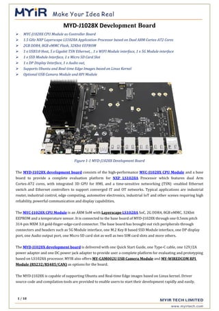
- 1. 1 / 10 MYD-J1028X Development Board MYC-J1028X CPU Module as Controller Board 1.5 GHz NXP Layerscape LS1028A Application Processor based on Dual ARM Cortex-A72 Cores 2GB DDR4, 8GB eMMC Flash, 32Kbit EEPROM 1 x USB3.0 Host, 5 x Gigabit TSN Ethernet, , 1 x WIFI Module interface, 1 x 5G Module interface 1 x SSD Module Interface, 1 x Micro SD Card Slot 1 x DP Display Interface, 1 x Audio out, Supports Ubuntu and Real-time Edge Images based on Linux Kernel Optional USB Camera Module and RPI Module Figure 1-1 MYD-J1028X Development Board The MYD-J1028X development board consists of the high-performance MYC-J1028X CPU Module and a base board to provide a complete evaluation platform for NXP LS1028A Processor which features dual Arm Cortex-A72 cores, with integrated 3D GPU for HMI, and a time-sensitive networking (TSN) -enabled Ethernet switch and Ethernet controllers to support converged IT and OT networks. Typical applications are industrial router, industrial control, edge computing, automotive electronics, industrial IoT and other scenes requiring high reliability, powerful communication and display capabilities. The MYC-J1028X CPU Module is an ARM SoM with Layerscape LS1028A SoC, 2G DDR4, 8GB eMMC, 32Kbit EEPROM and a temperature sensor. It is connected to the base board of MYD-J1028X through one 0.5mm pitch 314-pin MXM 3.0 gold-finger-edge-card connector. The base board has brought out rich peripherals through connectors and headers such as 5G Module interface, one M.2 Key B based SSD Module interface, one DP display port, one Audio output port, one Micro SD card slot as well as two SIM card slots and more others. The MYD-J1028X development board is delivered with one Quick Start Guide, one Type-C cable, one 12V/2A power adapter and one DC power jack adapter to provide user a complete platform for evaluating and prototyping based on LS1028A processor. MYIR also offers MY-CAM002U USB Camera Module and MY-WIREDCOM RPI Module (RS232/RS485/CAN) as options for the board. The MYD-J1028X is capable of supporting Ubuntu and Real-time Edge images based on Linux kernel. Driver source code and compilation tools are provided to enable users to start their development rapidly and easily.
- 2. 2 / 10 Figure 1-2 MYD-J1028X Development Board Top-view Figure 1-3 MYD-J1028X Development Board Bottom-view
- 3. 3 / 10 Hardware Specification The MYC-J1028X CPU Module is using NXP’s 17 x 17 x 2.46 mm, 0.75 mm pitch, FBGA448 of fine-pitch ball grid array package Layerscape LS1028A dual-core application processor (LS1028AXN7PQA). The LS1028A processor is equipped with TSN-enabled Ethernet switches and Ethernet controllers to support converged IT and OT networks. Two 64-bit Arm v8 cores provide industrial-controlled real-time processing and virtualization support for IoT edge computing. Integrated GPU and LCD controllers enable human-machine interface (HMI) systems to support new high-speed interfaces. The main features of Layerscape LS1028A processor are as follows: Dual Arm v8 Processors for Industrial Applications 4 port Time-Sensitive Networking enabled switch 2 Time-Sensitive Networking-capable Ethernet controllers GPU and LCD Controller Configurable cryptographic offload engines Integrated trust architecture PCI Express CAN Bus Figure 1-4 Layerscape LS1028A System Block Diagram
- 4. 4 / 10 The MYD-J1028X Development Board is using MYC-J1028X CPU Module as core controller board. It takes full features of NXP LS1028A processor and the main features are characterized as below: Mechanical Parameters • Dimensions: 150mm x 200mm (base board), 82mm x 45mm (CPU Module) • PCB Layers: 4-layer design (base board), 12-layer design (CPU Module) • Power supply: +12V/2A (base board), 5V/2A (CPU Module) • Working temperature: -40~85 Celsius (industrial grade) The MYD-J1028X Controller Board (MYC-J1028X CPU Module) Figure 1-5 MYC-J1028X CPU Module Top-view Figure 1-6 MYC-J1028X CPU Module Bottom-view
- 5. 5 / 10 Processor • NXP Layerscape LS1028A Dual-core Processor -1.5 GHz Dual-core ARM Cortex-A72 CPU (LS1028AXN7PQA, industrial grade) - Integrated TSN Ethernet switches and Ethernet controllers - Integrated GPU and LCD controller Memory • 2GB DDR4 ( supports 3GB / 4GB DDR4) • 8GB eMMC Flash (supports 16GB / 32GB eMMC) • 32Kbit EEPROM • QSPI Nand Flash (DNP by default) • XSPI NOR Flash (DNP by default) Peripherals and Signals Routed to Pins • Temperature Sensor • 0.5mm pitch 314-pin MXM 3.0 Gold-finger-edge-card Connector - 1 x SGMII signal and 1 x QSGMII signal - 2 x PCIe 3.0 and 1 x SATA 3.0 - 2 x CAN-FD - 2 x USB3.0 - 8 x I2C and 3 x SPI - 2 x SDIO - 2 x UART and 6 x LPUART - 1 x DP1.3/eDP1.4 (supports 4K@60fps) - 1 x JTAG - 6 x SAI - GPIOs Note: the peripheral signals brought out to the expansion interface are listed in maximum number. Some signals are reused. Please refer to the processor datasheet.
- 6. 6 / 10 The MYD-J1028X Development Board Base Board Figure 1-6 MYD-J1028X Development Board Base Board • 1 x Power Jack • 1 x Power Switch • Serial ports - 1 x Debug UART (TTL, USB Type-C connector) - 2 x TTL serial ports (brought out from expansion header) USB - 1 x USB 3.0 Host port - 1 x USB 3.0 based M.2 Key B 5G Module interface (J10) • 2 x SIM card slots • 5 x 10/100/1000 Mbps TSN Ethernet interfaces (RJ45) • 1 x M.2 Key E PCIe 3.0 based WiFi module interface (J14) • 1 x M.2 Key B SATA 3.0 based SSD Module interface (J13) • 1 x Micro SD card slot • 1 x DP Display port (supports DP1.3 and eDP1.4, resolution up to 4K@60FPS) • 1 x 3.5mm Audio Output interface • 1 x 2.54mm 2 x 20-pin male expansion header (J18, GPIO/I2C/SPI/UART/CAN, compatible with Raspberry PI standard 40-pin extension interface) Supports MYIR’s MY-WIREDCOM RPI Module through J18 to extend RS232, RS485 and RS232 functions • 2 x Buttons (one for Reset and one for User) • 1 x LED (Power on indicator: Green)
- 7. 7 / 10 Figure 1-7 MYC-J1028X CPU Module Function Block Diagram Figure 1-8 MYD-J1028X Development Board Function Block Diagram
- 8. 8 / 10 Figure 1-9 MYC-J1028X Dimensions Chart (Unit: MM) Figure 1-10 MYD-J1028X Base Board Dimensions Chart (Unit: MM)
- 9. 9 / 10 Software Features The MYD-J1028X development board is ready to run Linux which is provided with software package. Many peripheral drivers are in source code to help accelerate customer’s designs. The software package provided is characterized as following: Table 1-1 Linux Software Features Item Features Description Source Code Provided Bootstrap program RCW Initializing system clocks, PIN MUX YES ATF Switching between secure and unsafe environments, DDR initialization YES uboot u-boot 2020.04 YES Linux kernel Image Customized based on official Kernel_5.4.47 (Ubuntu) YES Custom based on official Kernel 5.10.9 (Edge) YES Drivers MMC eSDHC driver YES SPI SPI driver YES I2C I2C driver YES USB Host USB driver YES Ethernet Gigabit Ethernet driver YES DSA Switch Switch driver YES TSN TSN driver YES XPSI XPSI driver YES UART Serial driver YES CAN CAN driver YES GPIO GPIO driver YES RTC RTC driver YES SATA SATA driver YES PCIE PCIE driver YES SAI SAI driver YES DP DP driver YES File System Ubuntu Ubuntu file system built on LSDK 20.12 YES myir-image-full Edge file system built on Yocto 3.2.1 YES Compiler Tool Chain Cross compiler aarch64-linux-gnu-gcc BINARY
- 10. 10 / 10 Order Information Product Item Part No. Packing List MYD-J1028X Development Board MYD-J1028N-8E2D-150-I One MYD-J1028X Development Board (including MYC-J1028X CPU Module) One USB Type-A to Type-C cable One 12V/2A Power adapter One DC power jack adapter One Quick Start Guide MYC-J1028X CPU Module MYC-J1028N-8E2D-150-I Add-on Options MYC-J1028X CPU Module MY-CAM002U USB Camera Module MY-WIREDCOM RPI Module MY-CAM002U USB Camera MY-CAM002U MY-WIREDCOM RPI Module (RS232/RS485/CAN) MY-WIREDCOM MYIR Tech Limited Room 04, 6th Floor, Building No.2, Fada Road, Yunli Smart Park, Bantian, Longgang District, Shenzhen, Guangdong, China 518129 E-mail: sales@myirtech.com Phone: +86-755-22984836 Fax: +86-755-25532724 Website: http://www.myirtech.com