(ANVI) Koregaon Park Call Girls Just Call 7001035870 [ Cash on Delivery ] Pun...
irl530.pdf
1. IRL530
www.vishay.com
Vishay Siliconix
S21-1046-Rev. C, 25-Oct-2021 1 Document Number: 91299
For technical questions, contact: hvm@vishay.com
THIS DOCUMENT IS SUBJECT TO CHANGE WITHOUT NOTICE. THE PRODUCTS DESCRIBED HEREIN AND THIS DOCUMENT
ARE SUBJECT TO SPECIFIC DISCLAIMERS, SET FORTH AT www.vishay.com/doc?91000
Power MOSFET
FEATURES
• Dynamic dV/dt rating
• Repetitive avalanche rated
• Logic-level gate drive
• RDS(on) specified at VGS = 4 V and 5 V
• 175 °C operating temperature
• Fast switching
• Ease of paralleling
• Material categorization: for definitions of compliance
please see www.vishay.com/doc?99912
Note
* This datasheet provides information about parts that are
RoHS-compliant and / or parts that are non RoHS-compliant. For
example, parts with lead (Pb) terminations are not RoHS-compliant.
Please see the information / tables in this datasheet for details
DESCRIPTION
Third generation power MOSFETs from Vishay provide the
designer with the best combination of fast switching,
ruggedized device design, low on-resistance and cost
effectiveness.
The TO-220AB package is universally preferred for all
commercial-industrial applications at power dissipation
levels to approximately 50 W. The low thermal resistance
and low package cost of the TO-220AB contribute to its
wide acceptance throughout the industry.
Notes
a. Repetitive rating; pulse width limited by maximum junction temperature (see fig. 11)
b. VDD = 25 V, starting TJ = 25 °C, L = 1.9 mH, Rg = 25 Ω, IAS = 15 A (see fig. 12)
c. ISD ≤ 15 A, dI/dt ≤ 140 A/ms, VDD ≤ VDS, TJ ≤ 175 °C
d. 1.6 mm from case
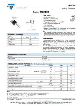
PRODUCT SUMMARY
VDS (V) 100
RDS(on) (Ω) VGS = 5.0 V 0.16
Qg (Max.) (nC) 28
Qgs (nC) 3.8
Qgd (nC) 14
Configuration Single
N-Channel MOSFET
G
D
S
TO-220AB
G
D
S
Available
Available
ORDERING INFORMATION
Package TO-220AB
Lead (Pb)-free IRL530PbF
Lead (Pb)-free and halogen-free IRL530PbF-BE3
ABSOLUTE MAXIMUM RATINGS (TC = 25 °C, unless otherwise noted)
PARAMETER SYMBOL LIMIT UNIT
Drain-source voltage VDS 100
V
Gate-source voltage VGS ± 10
Continuous drain current VGS at 5 V
TC = 25 °C
ID
15
A
TC = 100 °C 11
Pulsed drain current a IDM 60
Linear derating factor 0.59 W/°C
Single pulse avalanche energy b EAS 290 mJ
Repetitive avalanche current a IAR 15 A
Repetitive avalanche energy a EAR 8.8 mJ
Maximum power dissipation TC = 25 °C PD 88 W
Peak diode recovery dV/dt c dV/dt 5.5 V/ns
Operating junction and storage temperature range TJ, Tstg -55 to +175
°C
Soldering recommendations (peak temperature) d For 10 s 300 d
Mounting torque 6-32 or M3 screw
10 lbf · in
1.1 N · m
2. IRL530
www.vishay.com
Vishay Siliconix
S21-1046-Rev. C, 25-Oct-2021 2 Document Number: 91299
For technical questions, contact: hvm@vishay.com
THIS DOCUMENT IS SUBJECT TO CHANGE WITHOUT NOTICE. THE PRODUCTS DESCRIBED HEREIN AND THIS DOCUMENT
ARE SUBJECT TO SPECIFIC DISCLAIMERS, SET FORTH AT www.vishay.com/doc?91000
Notes
a. Repetitive rating; pulse width limited by maximum junction temperature (see fig. 11)
b. Pulse width ≤ 300 μs; duty cycle ≤ 2 %
THERMAL RESISTANCE RATINGS
PARAMETER SYMBOL TYP. MAX. UNIT
Maximum junction-to-ambient RthJA - 62
°C/W
Case-to-sink, flat, greased surface RthCS 0.50 -
Maximum junction-to-case (drain) RthJC - 1.7
SPECIFICATIONS (TJ = 25 °C, unless otherwise noted)
PARAMETER SYMBOL TEST CONDITIONS MIN. TYP. MAX. UNIT
Static
Drain-source breakdown voltage VDS VGS = 0 V, ID = 250 μA 100 - - V
VDS temperature coefficient ΔVDS/TJ Reference to 25 °C, ID = 1 mA - 0.14 - V/°C
Gate-source threshold voltage VGS(th) VDS = VGS, ID = 250 μA 1.0 - 2.0 V
Gate-source leakage IGSS VGS = ± 10 - - ± 100 nA
Zero gate voltage drain current IDSS
VDS = 100 V, VGS = 0 V - - 25
μA
VDS = 80 V, VGS = 0 V, TJ = 150 °C - - 250
Drain-source on-state resistance RDS(on)
VGS = 5.0 V ID = 9.0 Ab - - 0.16
Ω
VGS = 4.0 V ID = 7.5 Ab - - 0.22
Forward transconductance gfs VDS = 50 V, ID = 9.0 Ab 6.4 - - S
Dynamic
Input capacitance Ciss
VGS = 0 V,
VDS = 25 V,
f = 1.0 MHz, see fig. 5
- 930 -
pF
Output capacitance Coss - 250 -
Reverse transfer capacitance Crss - 57 -
Total gate charge Qg
VGS = 5.0 V
ID = 15 A, VDS = 80 V,
see fig. 6 and 13b
- - 28
nC
Gate-source charge Qgs - - 3.8
Gate-drain charge Qgd - - 14
Turn-on delay time td(on)
VDD = 50 V, ID = 15 A,
Rg = 12 Ω, RD = 32 Ω, see fig. 10b
- 4.7 -
ns
Rise time tr - 100 -
Turn-off delay time td(off) - 22 -
Fall time tf - 48 -
Internal drain inductance LD
Between lead,
6 mm (0.25") from
package and center of
die contact
- 4.5 -
nH
Internal source inductance LS - 7.5 -
Drain-Source Body Diode Characteristics
Continuous source-drain diode current IS
MOSFET symbol
showing the
integral reverse
p - n junction diode
- - 15
A
Pulsed diode forward current a ISM - - 60
Body diode voltage VSD TJ = 25 °C, IS = 15 A, VGS = 0 Vb - - 2.5 V
Body diode reverse recovery time trr
TJ = 25 °C, IF = 15 A, dI/dt = 100 A/μsb
- 150 200 ns
Body diode reverse recovery charge Qrr - 0.93 1.4 μC
Forward turn-on time ton Intrinsic turn-on time is negligible (turn-on is dominated by LS and LD)
D
S
G
S
D
G
3. IRL530
www.vishay.com
Vishay Siliconix
S21-1046-Rev. C, 25-Oct-2021 3 Document Number: 91299
For technical questions, contact: hvm@vishay.com
THIS DOCUMENT IS SUBJECT TO CHANGE WITHOUT NOTICE. THE PRODUCTS DESCRIBED HEREIN AND THIS DOCUMENT
ARE SUBJECT TO SPECIFIC DISCLAIMERS, SET FORTH AT www.vishay.com/doc?91000
TYPICAL CHARACTERISTICS (25 °C, unless otherwise noted)
Fig. 1 - Typical Output Characteristics, TC = 25 °C
Fig. 2 - Typical Output Characteristics, TC = 175 °C
Fig. 3 - Typical Transfer Characteristics
Fig. 4 - Normalized On-Resistance vs. Temperature
4. IRL530
www.vishay.com
Vishay Siliconix
S21-1046-Rev. C, 25-Oct-2021 4 Document Number: 91299
For technical questions, contact: hvm@vishay.com
THIS DOCUMENT IS SUBJECT TO CHANGE WITHOUT NOTICE. THE PRODUCTS DESCRIBED HEREIN AND THIS DOCUMENT
ARE SUBJECT TO SPECIFIC DISCLAIMERS, SET FORTH AT www.vishay.com/doc?91000
Fig. 5 - Typical Capacitance vs. Drain-to-Source Voltage
Fig. 6 - Typical Gate Charge vs. Gate-to-Source Voltage
Fig. 7 - Typical Source-Drain Diode Forward Voltage
Fig. 8 - Maximum Safe Operating Area
5. IRL530
www.vishay.com
Vishay Siliconix
S21-1046-Rev. C, 25-Oct-2021 5 Document Number: 91299
For technical questions, contact: hvm@vishay.com
THIS DOCUMENT IS SUBJECT TO CHANGE WITHOUT NOTICE. THE PRODUCTS DESCRIBED HEREIN AND THIS DOCUMENT
ARE SUBJECT TO SPECIFIC DISCLAIMERS, SET FORTH AT www.vishay.com/doc?91000
Fig. 9 - Maximum Drain Current vs. Case Temperature
Fig. 10a - Switching Time Test Circuit
Fig. 10b - Switching Time Waveforms
Fig. 11 - Maximum Effective Transient Thermal Impedance, Junction-to-Case
Pulse width ≤ 1 µs
Duty factor ≤ 0.1 %
RD
VGS
RG
D.U.T.
5 V
+
-
VDS
VDD
VDS
90 %
10 %
VGS
td(on) tr td(off) tf
6. IRL530
www.vishay.com
Vishay Siliconix
S21-1046-Rev. C, 25-Oct-2021 6 Document Number: 91299
For technical questions, contact: hvm@vishay.com
THIS DOCUMENT IS SUBJECT TO CHANGE WITHOUT NOTICE. THE PRODUCTS DESCRIBED HEREIN AND THIS DOCUMENT
ARE SUBJECT TO SPECIFIC DISCLAIMERS, SET FORTH AT www.vishay.com/doc?91000
Fig. 12a - Unclamped Inductive Test Circuit Fig. 12b - Unclamped Inductive Waveforms
Fig. 12c - Maximum Avalanche Energy vs. Drain Current
Fig. 13a - Basic Gate Charge Waveform Fig. 13b - Gate Charge Test Circuit
RG
IAS
0.01 Ω
tp
D.U.T
L
VDS
+
-
VDD
5 V
Vary tp to obtain
required IAS
IAS
VDS
VDD
VDS
tp
QGS QGD
QG
VG
Charge
5.0 V
D.U.T.
3 mA
VGS
VDS
IG ID
0.3 µF
0.2 µF
50 kΩ
12 V
Current regulator
Current sampling resistors
Same type as D.U.T.
+
-
7. IRL530
www.vishay.com
Vishay Siliconix
S21-1046-Rev. C, 25-Oct-2021 7 Document Number: 91299
For technical questions, contact: hvm@vishay.com
THIS DOCUMENT IS SUBJECT TO CHANGE WITHOUT NOTICE. THE PRODUCTS DESCRIBED HEREIN AND THIS DOCUMENT
ARE SUBJECT TO SPECIFIC DISCLAIMERS, SET FORTH AT www.vishay.com/doc?91000
Fig. 14 - For N-Channel
Vishay Siliconix maintains worldwide manufacturing capability. Products may be manufactured at one of several qualified locations. Reliability data for Silicon
Technology and Package Reliability represent a composite of all qualified locations. For related documents such as package/tape drawings, part marking, and
reliability data, see www.vishay.com/ppg?91299.
P.W.
Period
dI/dt
Diode recovery
dV/dt
Ripple ≤ 5 %
Body diode forward drop
Re-applied
voltage
Reverse
recovery
current
Body diode forward
current
VGS = 10 Va
ISD
Driver gate drive
D.U.T. lSD waveform
D.U.T. VDS waveform
Inductor current
D =
P.W.
Period
+
-
+
+
+
-
-
-
Peak Diode Recovery dV/dt Test Circuit
VDD
• dV/dt controlled by Rg
• Driver same type as D.U.T.
• ISD controlled by duty factor “D”
• D.U.T. - device under test
D.U.T.
Circuit layout considerations
• Low stray inductance
• Ground plane
• Low leakage inductance
current transformer
Rg
Note
a. VGS = 5 V for logic level devices
VDD
8. Package Information
www.vishay.com
Vishay Siliconix
Revison: 04-Nov-2021 1 Document Number: 66542
For technical questions, contact: hvm@vishay.com
THIS DOCUMENT IS SUBJECT TO CHANGE WITHOUT NOTICE. THE PRODUCTS DESCRIBED HEREIN AND THIS DOCUMENT
ARE SUBJECT TO SPECIFIC DISCLAIMERS, SET FORTH AT www.vishay.com/doc?91000
TO-220-1
Note
• M* = 0.052 inches to 0.064 inches (dimension including protrusion), heatsink hole for HVM
DIM.
MILLIMETERS INCHES
MIN. MAX. MIN. MAX.
A 4.24 4.65 0.167 0.183
b 0.69 1.02 0.027 0.040
b(1) 1.14 1.78 0.045 0.070
c 0.36 0.61 0.014 0.024
D 14.33 15.85 0.564 0.624
E 9.96 10.52 0.392 0.414
e 2.41 2.67 0.095 0.105
e(1) 4.88 5.28 0.192 0.208
F 1.14 1.40 0.045 0.055
H(1) 6.10 6.71 0.240 0.264
J(1) 2.41 2.92 0.095 0.115
L 13.36 14.40 0.526 0.567
L(1) 3.33 4.04 0.131 0.159
Ø P 3.53 3.94 0.139 0.155
Q 2.54 3.00 0.100 0.118
ECN: E21-0621-Rev. D, 04-Nov-2021
DWG: 6031
M*
3
2
1
L
L(1)
D
H(1)
Q
Ø P
A
F
J(1)
b(1)
e(1)
e
E
b
C