SiGe epitaxy on a 300 mm batch furnace
•
1 like•1,368 views

SiGe epitaxy on a 300 mm batch furnace, Presentation at The EuroCVD 18 conference will take place in Kinsale, County Cork, Ireland from the 4th – 9th September 2011

Recommended
More Related Content
Viewers also liked
Viewers also liked (19)
Similar to SiGe epitaxy on a 300 mm batch furnace
Similar to SiGe epitaxy on a 300 mm batch furnace (20)
Recently uploaded
Recently uploaded (20)
SiGe epitaxy on a 300 mm batch furnace
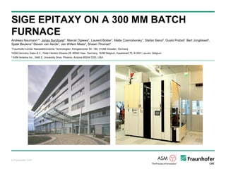
- 1. © Fraunhofer CNT SIGE EPITAXY ON A 300 MM BATCH FURNACE Andreas Naumann1*, Jonas Sundqvist1, Marcel Ogiewa1, Laurent Boitier1, Malte Czernohorsky1, Stefan Sienz2, Guido Probst2, Bert Jongbloed3, Sjaak Beulens3 Steven van Aerde3, Jan Willem Maes3, Shawn Thomas4 1Fraunhofer-Center Nanoelektronische Technologien, Königsbrücker Str. 180, 01099 Dresden, Germany 2ASM Germany Sales B.V., Peter-Henlein-Strasse 28, 85540 Haar, Germany, 3ASM Belgium, Kapeldreef 75, B-3001 Leuven, Belgium 4 ASM America Inc., 3440 E. University Drive, Phoenix, Arizona 85034-7200, USA
- 2. © Fraunhofer CNT Table of Content 1. Fraunhofer CNT 2. SiGe Epitaxy on ASM A412 300mm Batch Furnace 3. Characterization Results 4. Summary
- 3. © Fraunhofer CNT The Heart of Microelectronics in Europe… Area Dresden North
- 4. © Fraunhofer CNT Fraunhofer Center Nanoelectronic Technologies Docking Research into Manufacturing 800m2 Clean Room Area 200m2 Lab Area 40 Tools (Processing and Metrology/Analytics) External customers (IC manufacturers, Foundries) Platform for material and process development on 300mm Si wafer Short learning cycles Industrial-grade clean room Infrastructure Linked to 300mm production lines
- 5. © Fraunhofer CNT Table of Content 1. Fraunhofer CNT 2. Epitaxy on ASM A412 300mm Batch Furnace 3. Characterization Results 4. Summary
- 6. © Fraunhofer CNT Potential Batch Epi Applications 2011-09-20Confidential and Proprietary Information 6 S/D epi of cell transistor PCRAM diode Logic devices high mobility channel (Selective) SiGe + Si o (Selective) un-doped Ge source-drain stressor w/ doping Un-doped Si, SiGe o Doped Si, SiGe o Complex S/D epi designs questionable Memory DRAM peri source-drain stressor selective Si, SiGe DRAM access transistor S/D epi selective Si DRAM Bit Line Contact Selective SiGe PCRAM Diode Selective Si Solar Low cost of ownership solution Blanket (selective) Si (B, P, As doped)
- 7. © Fraunhofer CNT Motivation for Large Batch Furnace Si, SiGe Epitaxy Pro Reduced cost of ownership Less product sensitive Low temperature processing New applications (e.g. Solar) Con Process development challenging Less flexibility (cycle time penalty)
- 8. © Fraunhofer CNT ASM A412 300mm Furnace @ Fraunhofer CNT Properties of A412 Batch Furnace: Two reactors (TiN/TaCN + aSi, Poly, Si/SiGe EPI) Batch size up to 100 wafer (300mm) Inert minienvironment (< 10ppm O2) Internal stocker Atmospheric N2 loading ambient, i.e., no vacuum loadlock, which is more costly, complicated, and takes more (cycle) time. Epitaxy Setup on Reactor1: Max. temperature 900°C SiH4, GeH4, H2, N2, HCL available Base pressure <5 mTorr
- 9. © Fraunhofer CNT Target Demonstrate Feasibility of Batch Furnace for SiGe Epitaxy. Layer thickness 10 - 100 nm Germanium concentration 10 - 45 at.% Within wafer uniformity < 2% (1σ) (Ge concentration and layer thickness) Oxygen background at interface below SIMS detection limit ( < 1E12 O/cm²) Layer roughness < 0.2 nm RMS Demonstrate SEG (25 at.%, 50 nm, selective to oxide and nitride)
- 10. © Fraunhofer CNT Table of Content 1. Fraunhofer CNT 2. Epitaxy on ASM A412 300mm Batch Furnace 3. Characterization Results 4. Summary
- 11. © Fraunhofer CNT Surface Cleaning Clean conditions: HF last wet clean Insitu clean with H2 Temperature 800°C Low pressure 20 min With 800°C bake: Oxygen not detectable with ToFSIMS 0 200 400 600 800 1000 0 100 200 300 400 500 600 700 0 25 50 75 100 125 150 175 OxygenIntensity[cts/s] Sputter time [s] Oxygen [cts/s] 725°C Bake 775°C Bake 800°C Bake Sputter depth [nm] Oxygen free surface is a prerequisite for silicon epitaxy!
- 12. © Fraunhofer CNT Control of Layer Composition SiGe composition tuneable with gas mixture No penalty with layer properties 0 10 20 30 40 0 0.5 1 1.5 2 Germane flow [a.u.] Germaniumconcentration[at.%]
- 13. © Fraunhofer CNT Layer Uniformity Thickness: 50 nm, wiw 2.5% (1σ) Ge concentration: 25at.%, wiw 1.6% (1σ) Root cause gas depletion 1 2 3 4 5 6 7 8 9 10 11 12 13 14 15 16 17 18 19 20 21 22 23 24 25 2627 28 29 30 31 32 33 34 35 36 37 38 39 40 41 42 43 44 45 46 47 48 49 -150 -100 -50 0 50 100 150 -150 -100 -50 0 50 100 150 SiGelayer thickness(Run60) [nm] Y[mm] X [mm] 48,0 48,3 48,6 48,9 49,2 49,6 49,9 50,2 50,5 50,8 51,1 51,5 51,8 52,1 52,4 52,7 53,0 53,4 53,7 54,0 54,3 0 25 50 75 100 125 150 46 47 48 49 50 51 52 53 54 55 56 57 58 Layerthickness[nm] Wafer radius [mm] 23 24 25 26 GermaniumConcentration[at.%] 1 2 3 4 5 6 7 8 9 10 11 12 13 14 15 16 17 18 19 20 21 22 23 24 25 2627 28 29 30 31 32 33 34 35 36 37 38 39 40 41 42 43 44 45 46 47 48 49 -150 -100 -50 0 50 100 150 -150 -100 -50 0 50 100 150 Geconcentration(Run60) [at.%] Y[mm] X [mm] 23,6 23,7 23,8 23,8 23,9 24,0 24,1 24,1 24,2 24,3 24,4 24,4 24,5 24,6 24,7 24,8 24,8 24,9 25,0 25,1 25,1 Thickness [nm] Ge concentration [at.%]
- 14. © Fraunhofer CNT Layer Roughness Layer roughness similar compared to test wafer used. This example has a RMS of 0.17 nm
- 15. © Fraunhofer CNT Strain Analysis Sharp SiGe peak and thickness fringes in ω-2θ-scan No offset between SiGe-224 and Si-224 in h-direction of RSM SiGe layer is fully strained SiGe-224 Si-224
- 16. © Fraunhofer CNT Selective Epitaxial Growth (SEG) results Silicon SEG with DCS+H2 @ 680°C Selective to oxide But unselective to nitride Silicon nitride HM SiGe SEG with SiH4+GeH4+HCl @520°C Selective to oxide Ge concentration not yet on target
- 17. © Fraunhofer CNT Table of Content 1. Fraunhofer CNT 2. Epitaxy on ASM A412 300mm Batch Furnace 3. Characterization results 4. Summary
- 18. © Fraunhofer CNT March 17 2011 18 Rough throughput estimates Process: SiGe (25 atm%), thickness <50 nm 100 wafer load 30 minutes boat-out, boat-in 60 minutes temperature ramp up, bake, cool down < 30 minutes deposition 30 minutes overhead Through put: >40 wafers/hour/chamber (>80 wafers/hour/tool)
- 19. © Fraunhofer CNT Summary Accomplishments: Layer thickness 10 - 100 nm Germanium concentration 10 - 32 at.% Within wafer uniformity < 2.5% (1σ) (Ge concentration and layer thickness) Oxygen background at interface below SIMS detection limit ( < 1E12 O/cm²) Layer roughness < 0.2 nm RMS Si and SiGe grown selective to oxide Further Investigation: Uniformity optimization SiGe SEG with nitride and oxide hard mask Improved epitaxial quality for selective growth Insitu doping (B, P) (started) √ √ √ √ √ √
- 20. © Fraunhofer CNT Thank you !