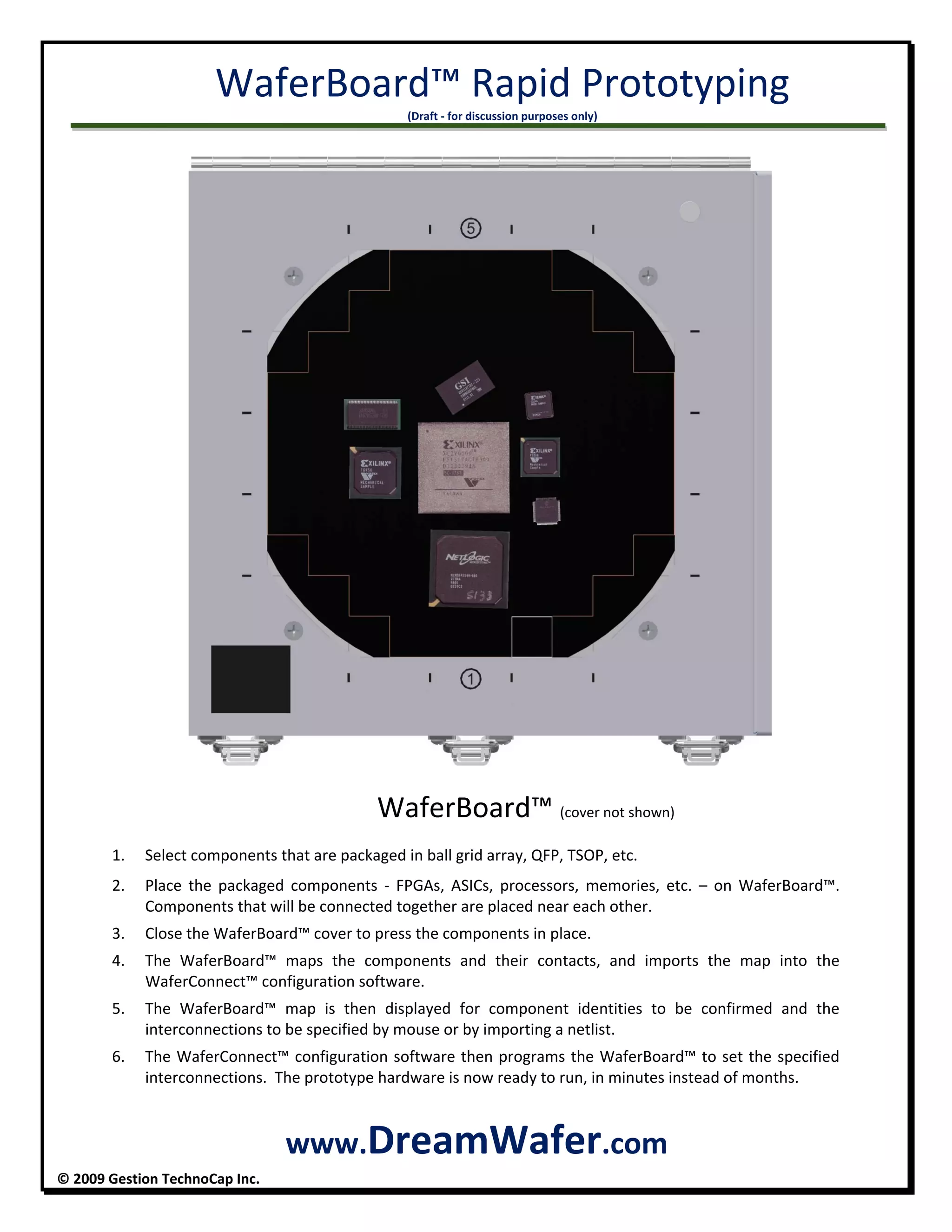
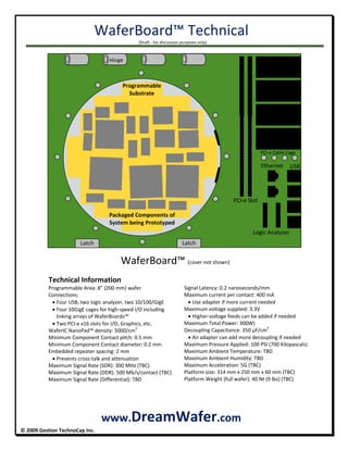
WaferBoard™ Rapid Prototyping                                              
(Draft ‐ for discussion purposes only) 
 
© 2009 Gestion TechnoCap Inc. 
 
                  WaferBoard™ (cover not shown) 
1. Select components that are packaged in ball grid array, QFP, TSOP, etc. 
2. Place  the  packaged  components  ‐  FPGAs,  ASICs,  processors,  memories,  etc.  –  on  WaferBoard™. 
Components that will be connected together are placed near each other. 
3. Close the WaferBoard™ cover to press the components in place. 
4. The  WaferBoard™  maps  the  components  and  their  contacts,  and  imports  the  map  into  the 
WaferConnect™ configuration software.  
5. The  WaferBoard™  map  is  then  displayed  for  component  identities  to  be  confirmed  and  the 
interconnections to be specified by mouse or by importing a netlist.   
6. The WaferConnect™ configuration software then programs the WaferBoard™ to set the specified 
interconnections.  The prototype hardware is now ready to run, in minutes instead of months. 
 
  www.DreamWafer.com 
WaferBoard™ for Electronic Systems 
      (Draft ‐ for discussion purposes only) 
 
               © 2009 Gestion TechnoCap Inc.  
 
WaferBoard™ Rapid Prototyping for Electronic Systems enhances creativity and invention and slashes 
prototyping  costs,  risks  and  time  to  market  by  allowing  hardware  from  simple  electronics  to  high‐
density electronics, micro‐nano systems or system‐on‐chip ASICs to be prototyped in minutes. 
 
A WaferBoard™ is a “waffle iron” for prototyping electronic systems. Simply place packaged components (“dough”) 
on the WaferBoard™ and close the cover.  The WaferBoard™ then senses the component contacts and recognizes 
the components and intelligently interconnects them (“cooks them”). The prototype (“waffle”) is now ready to be 
brought  up  and  run.  WaferBoard™  prototyping  can  save  the  electronic  systems  development  process  weeks  or 
months of time to market and tens to hundreds of thousands of dollars (or more). 
 
In developing new technologies for micro‐nano systems, displays, sensors, telecommunication devices, multimedia 
and computing systems; diverse components ranging from processors and memories, ASICs and FPGAs, analog and 
RF, photonics and sensors, and MEMs and microfluidics are interconnected to form complex systems.  Whether 
these electronics are the new technology or whether they merely support the new technology, The WaferBoard™ 
makes prototyping such systems simple by providing what these diverse components all need: power, ground and 
communications with each other and with the external world. 
 
Compared to traditional development, the WaferBoard™ approach is simple: 
1. Select components that are packaged in ball grid array, QFP, TSOP, etc. 
2. Place  the  packaged  components  ‐  FPGAs,  ASICs,  processors,  memories,  etc.  –  on  WaferBoard™, 
components that will be connected together are placed near each other. 
3. Close the WaferBoard™ cover to press the components in place. 
4. The WaferBoard™ maps the components and their contacts, and imports the map into the WaferConnect™ 
configuration software.  
5. The  WaferBoard™  map  is  then  displayed  for  component  identities  to  be  confirmed  and  the 
interconnections to be specified by mouse or by importing a netlist.   
6. The  WaferConnect™  configuration  software  then  programs  the  WaferBoard™  to  set  the  specified 
interconnections.  The prototype hardware is now ready to run. 
 
The  WaferBoard™  establishes  the  specified  control  and  data  connections  between  components,  and  supplies 
power to specified component contacts at controlled voltages.  WaferBoard™ built‐in PCI‐express and USB provide 
links to the external world.  User‐specific connections can also be added; non‐digital connections, such as analog 
sensors, antennae and micro‐fluidics, are not programmable but can be made directly to components if needed.  
 
Hardware  bring‐up  begins  immediately.    Debugging  is  simplified  –  any  signals  can  be  cloned  at  any  point,  and 
copies routed to software or to WaferBoard™ scope or logic analyzer connectors at any time.   Software integration 
starts early, and with a system that uses the actual components rather than emulation1
. 
 
1
 For SoC, where emulation is desired, partitioning is simplified by every FPGA connection being available where it is most useful. Complex hard IP (e.g. 
processors) can be used in component form when available to further speed prototype performance and peripherals can be added to replicate the SoC’s 
environment.  Thus software testing can proceed on a complete near‐real‐time prototype, allowing increased coverage while speeding time‐to‐market. 


www.DreamWafer.com 
WaferBoard™ for Researchers 
   (Draft ‐ for discussion purposes only) 
 
               © 2009 Gestion TechnoCap Inc.  
 
Imagine  it,  then  WaferBoard™  it.  The  WaferBoard™  enhances  creativity  by  removing  obstacles  to 
experimental  and  iterative  development.  Hand‐placing  packaged  components  is  sufficient  because 
WaferBoard™ detects and adapts to component position, connections can be made or removed at any 
time without worrying about signal integrity.  Components are added, moved or replaced as needed.  
 
1. Why a WaferBoard™ is essential for research 
The  WaferBoard™  is  essential  for  experimentation  because  it  lets  “what  if”  questions  be 
answered quickly.   Whether the system being prototyped is the research or whether it supports 
the research, the ability to rapidly and reprogrammably customize it to research needs speeds up 
the research process. 
 The FPGAs can be reprogrammed. 
 Custom ASICs can be added and integrated.  
 Commercial ASICs can be added and integrated.  
 All interconnections between FPGAs, memories, commercial and custom ASICs are 
completely reprogrammable at any time. 
 
2.  What do I the researcher do with it? 
Many systems simply require selecting the right FPGA‐to‐memory and FPGA‐to‐FPGA connections 
for the ‘hardware’, compiling C code to FPGA firmware, and the system is ready to run.  Right out 
of the box WaferBoard™ is an FPGA‐based development platform on steroids! 
 Select components that are packaged in ball grid array, QFP, TSOP, etc. 
 Programmable FPGA‐to‐memory connectivity allows custom algorithms to be prototyped.  
 Custom FPGA accelerators can give super‐computer performance on a desk‐top platform. 
Other research systems are centered on custom ASICs, but need supporting logic and memories. 
 The WaferBoard™ Central User Area allows high‐pin‐count customer or commercial to be 
densely inter‐connected with the supplied FPGAs and memories. 
 The  WaferBoard™  User  Areas  allow  custom  PACKAGED  chip  sets  to  be  added  and 
reprogrammably interconnected to each other and to the supplied FPGAs and memories.  
Testing of experimental systems is enhanced, too; the WaferBoard™ provides the ability to clone 
any signals at any point and display them using its virtual logic analyzer software. 
 
3. What tools do I need? 
Only a desk‐top or lap‐top computer and your research goals! 
 The WaferBoard™ WaferConnect™ software lets all system interconnections be specified 
through  its  intuitive  graphical  interface,  supplied  libraries  provide  the  basic  memory 
controllers  and  customizable  FPGA‐to‐FPGA  connections,  the  CMC‐supplied  FPGA  tools 
allow compiling RTL, Verilog, VHDL  or C algorithms to FPGA firmware. 
 If you already have system design tools, the WaferConnect™ software will import netlist 
files from PCB tools, configuration bit‐streams from FPGA tools, ASIC descriptions from 
parts libraries, and will export cloned signals to logic analyzer connectors.   
 
 
www.DreamWafer.com 
 WaferBoard™ for FPGAs 
   (Draft ‐ for discussion purposes only) 
 
               © 2009 Gestion TechnoCap Inc.  


    WaferBoard™ FPGA Platform (cover not shown) 
  
1. User Area is for packaged components of system being prototyped 
 The larger user areas are on the sides for easy access and support complex custom packaged chip sets 
              and peripherals for the system being prototyped. 
 
2. Central User Area is for packaged components needing the fastest access to FPGAs e.g. custom ASICs  
 If the prototype needs specialized chips, the central user area is ideal for a high‐performance user ASIC,   
    being close to all the large FPGAs and a variety of fast memories (with bulk RAM available further away). 
 
3. Flex PCB Cable (optional) is greater than 100 connections per cm
2
 
 ADC/DAC, custom I/O, optics, etc. 
 
4. Support PCB Underside includes Control CPU, PCI‐e Switch, Flash memory and DIMMS 


www.DreamWafer.com 
Any chip can be reprogrammably connected to any other chips; this flexibility makes 
the FPGAs and memories by themselves sufficient for prototyping many systems. 
  USB
    PCI‐e Slot 
Logic Analyzer
  PCI‐e Cable Cage
UserArea
1 
User Area
1
 
User Area
1 
Central 
User Area2
 
RLDRAM 
RLDRAM 
FPGA 
 
QDR 
FPGA 
FPGA 
FPGA 
RLDRAM 
 
QDR
 
QDR
QDR  QDR 
 
QDR
 
QDR 
 
RLDRAM 
RLDRAM 
RLDRAM 
RLDRAM 
RAM 
 
QDR
 
QDR
 
QDR
QDRQDR
RLDRAM 
RAM  RAM  RAM  RAM 
RAM RAM  RAM  RAM 
RAM  RAM 
RLDRAM 
RLDRAM 
RLDRAM 
RLDRAM 
Flex PCB Cable3 
(Optional)
 
 
Latch  Latch 
  Hinge
Support PCB 
Ethernet
  WaferIC™ 
Details 
    (Draft ‐ for discussion purposes only) 
 
© 2009 Gestion TechnoCap Inc.  
 
 
                         www.DreamWafer.com 
Z-Axis Film
Wafer 
TSV Layers 
Power Blocks
Back Plate
Reticle 
 WaferIC™ 
Numbers 
                                                                              (Draft ‐ for discussion purposes only) 
 
© 2009 Gestion TechnoCap Inc. 
 
The WaferIC™ is a wafer scale FPGA 
One WaferIC™ includes: 
 
                                  1   Wafer which is a single chip of 24,500 mm2
                                  1   Z-axis Film
                                21   PowerBlocks active (plus 4 filler triangles in corners)
                                  1   BackPlate
                                76   Reticles active (plus 8 blank partial reticles in corners)
                          4,864   Through Silicon Vias TSVs (8x8=64 per reticle)
                        77,824   Solder Bumps (4x4=16 per TSV)
                  1,245,184   Nanopads (128x128=16,384 per reticle)
                80,000,000   Z-axis Fibers (8x8=64 per nanopad)
                     155,648   User Component Distinct Connection Points (two per 4x4=16 nanopads)
                  1,477,120   Millimeter-scale programmable interconnection segments (20 per 4x4 nanopads, minus edges)
                          9,850   Meters of millimeter-scale programmable interconnection segments
                  1,710,848   Sub-millimeter programmable interconnect segments (22 per 4x4 nanopads, minus edges)
                             510   Meters of sub-millimeter programmable interconnection segments
                22,750,000   Bits of configuration memory
          1,900,000,000   Microns of gate width in programmable power transistors


                          www.DreamWafer.com 
WaferBoard™ Technical 
      (Draft ‐ for discussion purposes only) 
 
© 2009 Gestion TechnoCap Inc.  


   WaferBoard™ (cover not shown) 
 
Technical Information
                  Programmable Area: 8” (200 mm) wafer 
   Connections: 
 Four USB, two logic analyzer, two 10/100/GigE 
 Four 10GigE cages for high‐speed I/O including  
   linking arrays of WaferBoards™ 
 Two PCI‐e x16 slots for I/O, Graphics, etc. 
                      WaferIC NanoPad™ density: 5000/cm2
  
                      Minimum Component Contact pitch: 0.5 mm 
                      Minimum Component Contact diameter: 0.2 mm 
                      Embedded repeater spacing: 2 mm 
 Prevents cross‐talk and attenuation 
                      Maximum Signal Rate (SDR): 300 MHz (TBC) 
                      Maximum Signal Rate (DDR): 500 Mb/s/contact (TBC) 
                      Maximum Signal Rate (Differential): TBD 
 
www.DreamWafer.com 
Signal Latency: 0.2 nanoseconds/mm 
Maximum current per contact: 400 mA 
 Use adapter if more current needed 
Maximum voltage supplied: 3.3V 
 Higher‐voltage feeds can be added if needed 
Maximum Total Power: 300W) 
Decoupling Capacitance: 350 µF/cm2
  
 An adapter can add more decoupling if needed 
Maximum Pressure Applied: 100 PSI (700 Kilopascals) 
Maximum Ambient Temperature: TBD 
Maximum Ambient Humidity: TBD 
Maximum Acceleration: 5G (TBC) 
Platform size: 314 mm x 250 mm x 60 mm (TBC) 
Platform Weight (full wafer): 40 Nt (9 lbs) (TBC) 
  USB


Hinge  
    PCI‐e Slot 
Logic Analyzer
  PCI‐e Cable Cage
Latch  Latch 
Packaged Components of 
System being Prototyped
Programmable 
Substrate
  USBEthernet
WaferBoard™ Details 
  (Draft ‐ for discussion purposes only) 
 
© 2009 Gestion TechnoCap Inc.  
 
 
                           www.DreamWafer.com 
WaferIC™
Pouch
Top PCB
Power Supply
Bottom PCB

WaferBoard