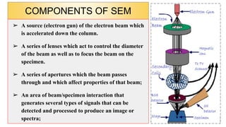
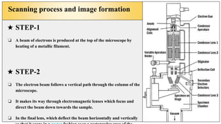
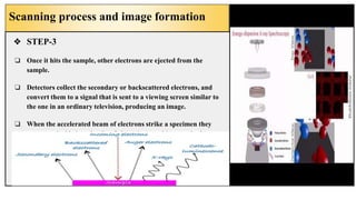
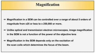
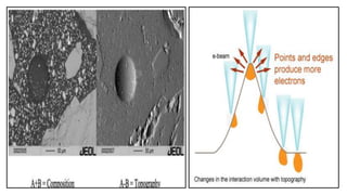
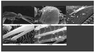
Scanning Electron
Microscopy-SEM
Submitted to - Dr. Alok Kumar
Submitted by-
Piyush Tripathi
2016MSES008
M.SC.-3rd
Semester
Department of
Environmental Science
Electron Microscope
★ The electron microscope is a type of microscope that uses a
beam of electrons to create an image of the specimen.
★ Have a higher resolving power than light microscope and can
reveal the structure of smaller objects.
★ Electrons are very sensitive to magnetic fields and can
therefore be controlled by changing the current through the
lenses.
★ Used to investigate the ultrastructure of a wide range of
biological and inorganic specimens including cells,
Microorganisms, biopsy samples, metals, and crystals.
SEM v/s TEM
❖ SEM=Scanning Electron Microscope and TEM Transmission Electron Microscope
❖ SEM is based on scattered electrons while TEM is based on transmitted electrons.
❖ SEM focuses on the sample’s surface and its composition whereas TEM provides the
details about internal composition.
❖ SEM allows for large amount of sample to be analysed at a time whereas with TEM
only small amount of sample can be analysed at a time.
❖ SEM also provides a 3-dimensional image while TEM provides a 2-dimensional
Scanning Electron Microscope - SEM
❏ Von Ardenne first constructed STEM in 1938
by rastering the electron beam in a TEM
followed by first commercial SEM in 1965.
❏ The typical scanning electron microscope
laboratory contains a machine with 2
components:
❏ 1. the microscope column, including the electron gun
at the top, the column, down which the electron beam
travels, and the sample chamber at the base.
❏ 2. the computer that drives the microscope, with the
additional bench controls
Principle:
When the accelerated primary
electrons strikes the sample , it produces
secondary electrons . these secondary
electrons are collected by a positive
charged electron detector which in turn
gives a 3- dimensional image of the
sample.
SEM- continue…..
❏ SEM images the sample surface by scanning it with a high-energy beam of
electrons in a raster scan pattern.
❏ The electrons interact with sample atoms producing signals that contain
information about the sample's surface topography, composition and other
properties such as electrical conductivity.
❏ The types of signals made by an SEM can include secondary electrons,
backscattered electrons, characteristic x-rays and light (cathodoluminescence).
COMPONENTS OF SEM
➢ A source (electron gun) of the electron beam which
is accelerated down the column.
➢ A series of lenses which act to control the diameter
of the beam as well as to focus the beam on the
specimen.
➢ A series of apertures which the beam passes
through and which affect properties of that beam;
➢ An area of beam/specimen interaction that
generates several types of signals that can be
detected and processed to produce an image or
spectra;
Scanning process and image formation
★ STEP-1
❏ A beam of electrons is produced at the top of the microscope by
heating of a metallic filament.
★ STEP-2
❏ The electron beam follows a vertical path through the column of the
microscope.
❏ It makes its way through electromagnetic lenses which focus and
direct the beam down towards the sample.
❏ In the final lens, which deflect the beam horizontally and vertically
Scanning process and image formation
❖ STEP-3
❏ Once it hits the sample, other electrons are ejected from the
sample.
❏ Detectors collect the secondary or backscattered electrons, and
convert them to a signal that is sent to a viewing screen similar to
the one in an ordinary television, producing an image.
❏ When the accelerated beam of electrons strike a specimen they
penetrate inside it to depths of about 1 μm and interact both
elastically and inelastically with the solid, from which various types
of radiation emerges -
Magnification
➔ Magnification in a SEM can be controlled over a range of about 5 orders of
magnitude from x25 or less to x 250,000 or more.
➔ Unlike optical and transmission electron microscopes, image magnification
in the SEM is not a function of the power of the objective lens
➔ Magnification in the SEM depends only on the excitation of
the scan coils which determines the focus of the beam.
Sample Preparation
❖ Starters-
samples need to be coated to make them conductive. Most often, a thin layer of gold
works.
❖ Sample Cleaning-
A clean sample is essential for image clarity.
For biological samples, use appropriate buffers or distilled water for cleaning the
samples. Use a surfactant if the sample requires more vigorous cleaning like in
metals.
❖ Sample Fixation and Dehydration
Use a fixative like glutaraldehyde or osmium vapor to maintain the structural details
of the sample.
Sample Preparation cont…..
❖ Drying-
➢ Prior to placing the sample in a high vacuum environment, it must be totally dry.
Otherwise, water vaporization will obstruct the electron beam and interfere with
image clarity.
➢ When using biological samples, be careful when doing critical point drying (or CPD),
so as to not compromise the structural integrity of the sample.
➢ freeze drying causes the least amount of sample shrinkage in comparison to air
drying or critical point drying. However, freeze drying carries the risk of ice crystal
Interference and Troubleshooting
Charging
Interference- Charging is produced by buildup of electrons in the sample and
their uncontrolled discharge, and can produce unwanted artefacts, particularly in
secondary electron images.
❖ When the number of incident electrons is greater than the number of electrons
escaping from the specimen, then a negative charge builds up at the point where the
beam hits the sample.
Troubleshooting -The level of charge will relate to the energy and the number
of electrons. The energy of the electrons is related to the kV so reducing kV can
reduce charging. And The number of electrons relates to parameters including, the
emission level of the gun, the spot size, and the apertures between the gun and the
specimen. So reducing the number of electrons by adjusting these parameters can also
reduce charging.
Edge effects
Interference-
❖ Edge effects are due to the enhanced emission of electrons from edges and peaks
within the specimen.
❖ They are caused by the effects of topography on the generation of secondary
electrons and are what gives form and outline to the images produced by the
Secondary Electron detector.
❖ Poor signal intensity occurs in those regions shielded from the detector, such as
depressions.
❖ Troubleshooting--Topographic contrast is also enhanced by Backscattered
electrons emitted from regions of the sample facing towards the detector.
False Sample Touch Alarms
Interference-
❖ We will usually get a false alarm when we are loading the sample into the chamber.
Troubleshooting -
❖ If we get a Sample Touch alarm when the system under vacuum, check the monitor
to make sure the sample is not touching the sides or top of the chamber.
Lack of detail of surface structures
Interference-
❖ At high kV the beam penetration and diffusion become larger and result in signal
(electrons coming out of the sample) being generated from deeper within the
specimen. This can obscure fine surface structures.
❖ It will also increase BSE and so the image will start to show changes in contrast based
on composition.
Troubleshooting-
The solution therefore, for obtaining fine surface structure is to exclude these
backscattered electrons by using lower kVs such as 3-10kV. Hence lower energy provides
better detail of surface structure.
Specimen damage
Interference-
❖ Irradiating a specimen with an electron beam results in a loss of the beam energy to
the sample in the form of heat.
❖ A higher kV results in a higher temperature at the irradiated point and this can
damage (e.g. melt) fragile specimens, such as polymers or proteins, and volatilise
waxes or other sample components.
❖ This can ruin a sample (as well as contaminate the SEM chamber).
Troubleshooting-
❖ The solution is to lower the beam energy, sometimes down to a few kV.
Biological samples Shrinking
Interference-
❏ Some tissues might shrink when excised.
Troubleshooting-
❏ It might be desirable to keep the tissue at its physiological length during
the fixation process
❏ use glutaraldehyde-cacodylate fixative,
Low contrast of cellular structures
Interference-
❏ Insufficient stain
Troubleshooting
❏ Tannic acid is a mordant and can improve the staining.
References
1. Michler, Goerg H. "Scanning electron microscopy (SEM)." (2008): 87-120.
2. Reed, Stephen Jervis Brent, and Stephen Jarvis Brent Reed. Electron microprobe analysis.
Vol. 2. Cambridge: Cambridge University Press, 1975.
3. Lee, Robert Edward. Scanning electron microscopy and X-ray microanalysis. PTR
Prentice Hall, 1993.
4. Reimer, Ludwig. "Scanning electron microscopy: physics of image formation and
microanalysis." (2000): 1826.
5. Google photos.
THANK YOU !

Scanning electron microscopy-SEM

  • 1.
    Scanning Electron Microscopy-SEM Submitted to- Dr. Alok Kumar Submitted by- Piyush Tripathi 2016MSES008 M.SC.-3rd Semester Department of Environmental Science
  • 2.
    Electron Microscope ★ Theelectron microscope is a type of microscope that uses a beam of electrons to create an image of the specimen. ★ Have a higher resolving power than light microscope and can reveal the structure of smaller objects. ★ Electrons are very sensitive to magnetic fields and can therefore be controlled by changing the current through the lenses. ★ Used to investigate the ultrastructure of a wide range of biological and inorganic specimens including cells, Microorganisms, biopsy samples, metals, and crystals.
  • 3.
    SEM v/s TEM ❖SEM=Scanning Electron Microscope and TEM Transmission Electron Microscope ❖ SEM is based on scattered electrons while TEM is based on transmitted electrons. ❖ SEM focuses on the sample’s surface and its composition whereas TEM provides the details about internal composition. ❖ SEM allows for large amount of sample to be analysed at a time whereas with TEM only small amount of sample can be analysed at a time. ❖ SEM also provides a 3-dimensional image while TEM provides a 2-dimensional
  • 4.
    Scanning Electron Microscope- SEM ❏ Von Ardenne first constructed STEM in 1938 by rastering the electron beam in a TEM followed by first commercial SEM in 1965. ❏ The typical scanning electron microscope laboratory contains a machine with 2 components: ❏ 1. the microscope column, including the electron gun at the top, the column, down which the electron beam travels, and the sample chamber at the base. ❏ 2. the computer that drives the microscope, with the additional bench controls
  • 5.
    Principle: When the acceleratedprimary electrons strikes the sample , it produces secondary electrons . these secondary electrons are collected by a positive charged electron detector which in turn gives a 3- dimensional image of the sample.
  • 6.
    SEM- continue….. ❏ SEMimages the sample surface by scanning it with a high-energy beam of electrons in a raster scan pattern. ❏ The electrons interact with sample atoms producing signals that contain information about the sample's surface topography, composition and other properties such as electrical conductivity. ❏ The types of signals made by an SEM can include secondary electrons, backscattered electrons, characteristic x-rays and light (cathodoluminescence).
  • 7.
    COMPONENTS OF SEM ➢A source (electron gun) of the electron beam which is accelerated down the column. ➢ A series of lenses which act to control the diameter of the beam as well as to focus the beam on the specimen. ➢ A series of apertures which the beam passes through and which affect properties of that beam; ➢ An area of beam/specimen interaction that generates several types of signals that can be detected and processed to produce an image or spectra;
  • 8.
    Scanning process andimage formation ★ STEP-1 ❏ A beam of electrons is produced at the top of the microscope by heating of a metallic filament. ★ STEP-2 ❏ The electron beam follows a vertical path through the column of the microscope. ❏ It makes its way through electromagnetic lenses which focus and direct the beam down towards the sample. ❏ In the final lens, which deflect the beam horizontally and vertically
  • 9.
    Scanning process andimage formation ❖ STEP-3 ❏ Once it hits the sample, other electrons are ejected from the sample. ❏ Detectors collect the secondary or backscattered electrons, and convert them to a signal that is sent to a viewing screen similar to the one in an ordinary television, producing an image. ❏ When the accelerated beam of electrons strike a specimen they penetrate inside it to depths of about 1 μm and interact both elastically and inelastically with the solid, from which various types of radiation emerges -
  • 10.
    Magnification ➔ Magnification ina SEM can be controlled over a range of about 5 orders of magnitude from x25 or less to x 250,000 or more. ➔ Unlike optical and transmission electron microscopes, image magnification in the SEM is not a function of the power of the objective lens ➔ Magnification in the SEM depends only on the excitation of the scan coils which determines the focus of the beam.
  • 11.
    Sample Preparation ❖ Starters- samplesneed to be coated to make them conductive. Most often, a thin layer of gold works. ❖ Sample Cleaning- A clean sample is essential for image clarity. For biological samples, use appropriate buffers or distilled water for cleaning the samples. Use a surfactant if the sample requires more vigorous cleaning like in metals. ❖ Sample Fixation and Dehydration Use a fixative like glutaraldehyde or osmium vapor to maintain the structural details of the sample.
  • 12.
    Sample Preparation cont….. ❖Drying- ➢ Prior to placing the sample in a high vacuum environment, it must be totally dry. Otherwise, water vaporization will obstruct the electron beam and interfere with image clarity. ➢ When using biological samples, be careful when doing critical point drying (or CPD), so as to not compromise the structural integrity of the sample. ➢ freeze drying causes the least amount of sample shrinkage in comparison to air drying or critical point drying. However, freeze drying carries the risk of ice crystal
  • 13.
  • 14.
    Charging Interference- Charging isproduced by buildup of electrons in the sample and their uncontrolled discharge, and can produce unwanted artefacts, particularly in secondary electron images. ❖ When the number of incident electrons is greater than the number of electrons escaping from the specimen, then a negative charge builds up at the point where the beam hits the sample. Troubleshooting -The level of charge will relate to the energy and the number of electrons. The energy of the electrons is related to the kV so reducing kV can reduce charging. And The number of electrons relates to parameters including, the emission level of the gun, the spot size, and the apertures between the gun and the specimen. So reducing the number of electrons by adjusting these parameters can also reduce charging.
  • 15.
    Edge effects Interference- ❖ Edgeeffects are due to the enhanced emission of electrons from edges and peaks within the specimen. ❖ They are caused by the effects of topography on the generation of secondary electrons and are what gives form and outline to the images produced by the Secondary Electron detector. ❖ Poor signal intensity occurs in those regions shielded from the detector, such as depressions. ❖ Troubleshooting--Topographic contrast is also enhanced by Backscattered electrons emitted from regions of the sample facing towards the detector.
  • 16.
    False Sample TouchAlarms Interference- ❖ We will usually get a false alarm when we are loading the sample into the chamber. Troubleshooting - ❖ If we get a Sample Touch alarm when the system under vacuum, check the monitor to make sure the sample is not touching the sides or top of the chamber.
  • 17.
    Lack of detailof surface structures Interference- ❖ At high kV the beam penetration and diffusion become larger and result in signal (electrons coming out of the sample) being generated from deeper within the specimen. This can obscure fine surface structures. ❖ It will also increase BSE and so the image will start to show changes in contrast based on composition. Troubleshooting- The solution therefore, for obtaining fine surface structure is to exclude these backscattered electrons by using lower kVs such as 3-10kV. Hence lower energy provides better detail of surface structure.
  • 18.
    Specimen damage Interference- ❖ Irradiatinga specimen with an electron beam results in a loss of the beam energy to the sample in the form of heat. ❖ A higher kV results in a higher temperature at the irradiated point and this can damage (e.g. melt) fragile specimens, such as polymers or proteins, and volatilise waxes or other sample components. ❖ This can ruin a sample (as well as contaminate the SEM chamber). Troubleshooting- ❖ The solution is to lower the beam energy, sometimes down to a few kV.
  • 19.
    Biological samples Shrinking Interference- ❏Some tissues might shrink when excised. Troubleshooting- ❏ It might be desirable to keep the tissue at its physiological length during the fixation process ❏ use glutaraldehyde-cacodylate fixative,
  • 20.
    Low contrast ofcellular structures Interference- ❏ Insufficient stain Troubleshooting ❏ Tannic acid is a mordant and can improve the staining.
  • 23.
    References 1. Michler, GoergH. "Scanning electron microscopy (SEM)." (2008): 87-120. 2. Reed, Stephen Jervis Brent, and Stephen Jarvis Brent Reed. Electron microprobe analysis. Vol. 2. Cambridge: Cambridge University Press, 1975. 3. Lee, Robert Edward. Scanning electron microscopy and X-ray microanalysis. PTR Prentice Hall, 1993. 4. Reimer, Ludwig. "Scanning electron microscopy: physics of image formation and microanalysis." (2000): 1826. 5. Google photos.
  • 24.