This document discusses power electronics and provides an overview of key concepts:
1. Power electronics refers to controlling and converting electrical power using power semiconductor devices like SCRs. Main applications include rectification, inversion, DC-DC conversion, and AC-AC conversion.
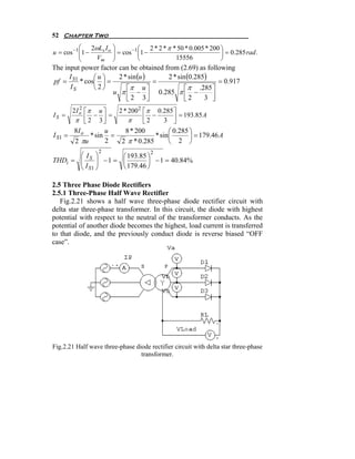
2. Rectification can be uncontrolled using diodes or controlled using SCRs. Common rectifier configurations include single and three-phase bridge rectifiers. Inversion converts DC to AC using devices like SCRs, IGBTs, and MOSFETs.
3. DC-DC conversion is commonly done using switch-mode power supplies with devices like BJTs and MOSFETs. AC-AC conversion using cycloconverters


![6 Chapter One
“Harmonics”. Also, the harmonics can be defined as a sinusoidal
component of a periodic waves or quality having frequencies that are an
integral multiple of the fundamental frequency.
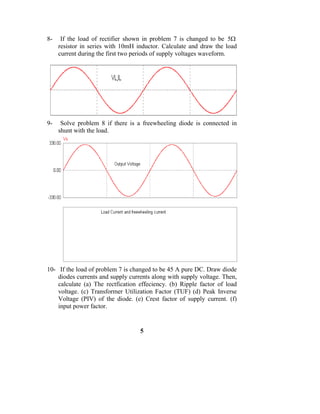
Among the devices that can generate nonlinear currents transformers
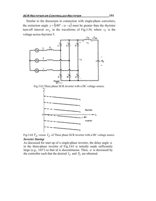
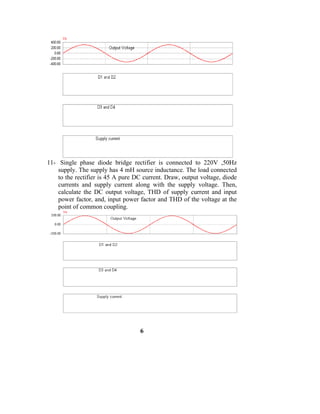
and induction machines (Because of magnetic core saturation) and power
electronics assemblies.
The electric utilities recognized the importance of harmonics as early
as the 1930’s such behavior is viewed as a potentially growing concern in
modern power distribution network.
1.7.1 Harmonics Effects on Power System Components
There are many bad effects of harmonics on the power system
components. These bad effects can derated the power system component
or it may destroy some devices in sever cases [Lee]. The following is the
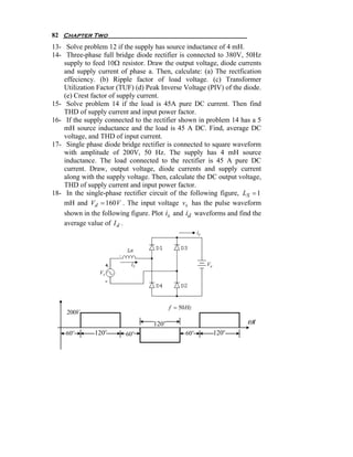
harmonic effects on power system components.
In Transformers and Reactors
• The eddy current losses increase in proportion to the square of the
load current and square harmonics frequency,
• The hysterics losses will increase,
• The loading capability is derated by harmonic currents , and,
• Possible resonance may occur between transformer inductance and
line capacitor.
In Capacitors
• The life expectancy decreases due to increased dielectric losses
that cause additional heating, reactive power increases due to
harmonic voltages, and,
• Over voltage can occur and resonance may occur resulting in
harmonic magnification.
In Cables
• Additional heating occurs in cables due to harmonic currents
because of skin and proximity effects which are function of
frequency, and,
• The I2R losses increase.
In Switchgear
• Changing the rate of rise of transient recovery voltage, and,
• Affects the operation of the blowout.
In Relays
• Affects the time delay characteristics, and,](https://image.slidesharecdn.com/powerelectronicsnote-121011031400-phpapp02/85/Power-electronics-note-9-320.jpg)
![Introduction 7
• False tripping may occurs.
In Motors
• Stator and rotor I2R losses increase due to the flow of harmonic
currents,
• In the case of induction motors with skewed rotors the flux
changes in both the stator and rotor and high frequency can
produce substantial iron losses, and,
• Positive sequence harmonics develop shaft torque that aid shaft
rotation; negative sequence harmonics have opposite effect.
In Generators
• Rotor and stator heating ,
• Production of pulsating or oscillating torques, and,
• Acoustic noise.
In Electronic Equipment
• Unstable operation of firing circuits based on zero voltage
crossing,
• Erroneous operation in measuring equipment, and,
• Malfunction of computers allied equipment due to the presence of
ac supply harmonics.
1.7.2 Harmonic Standards
It should be clear from the above that there are serious effects on the
power system components. Harmonics standards and limits evolved to
give a standard level of harmonics can be injected to the power system
from any power system component. The first standard (EN50006) by
European Committee for Electro-technical Standardization (CENELEE)
that was developed by 14th European committee. Many other
standardizations were done and are listed in IEC61000-3-4, 1998 [1].
The IEEE standard 519-1992 [2] is a recommended practice for power
factor correction and harmonic impact limitation for static power
converters. It is convenient to employ a set of analysis tools known as
Fourier transform in the analysis of the distorted waveforms. In general, a
non-sinusoidal waveform f(t) repeating with an angular frequency ω can
be expressed as in the following equation.
a0 ∞
f (t ) = + ∑ (a n cos(nωt ) + bn sin( nωt ) ) (1.1)
2 n=1](https://image.slidesharecdn.com/powerelectronicsnote-121011031400-phpapp02/85/Power-electronics-note-10-320.jpg)
![8 Chapter One
2π
1
where a n =
π ∫ f (t ) cos (nωt ) dωt (1.2)
0
2π
1
and bn =
π ∫ f (t ) sin (nωt ) dωt (1.3)
0
Each frequency component n has the following value
f n (t ) = a n cos ( nωt ) + bn sin (nωt ) (1.4)
fn(t) can be represented as a phasor in terms of its rms value as shown in
the following equation
a n + bn
2 2
Fn = e jϕ n (1.5)
2
− bn
Where ϕ n = tan −1 (1.6)
an
The amount of distortion in the voltage or current waveform is
qualified by means of an Total Harmonic Distortion (THD). The THD in
current and voltage are given as shown in (1.7) and (1.8) respectively.
2
Is − I s1
2 ∑ I sn
2
n≠n
THDi = 100 * = 100 * (1.7)
I s1 I s1
Vs2 − Vs2
∑Vsn
2
1 n≠n
THDv = 100 * = 100 * (1.8)
Vs1 Vs1
Where THDi & THDv The Total Harmonic Distortion in the current
and voltage waveforms
Current and voltage limitations included in the update IEE 519 1992
are shown in Table(1.1) and Table(1.2) respectively [2].
Table (1.1) IEEE 519-1992 current distortion limits for general distribution
systems (120 to 69kV) the maximum harmonic current distortion in percent of I L
Individual Harmonic order (Odd Harmonics)
I SC / I L n<11 11≤ n<17 17≤ n<23 23≤ n<35 35≤ n< TDD
<20 4.0 2.0 1.5 0.6 0.3 5.0
20<50 7.0 3.5 2.5 1.0 0.5 8.0
50<100 10.0 4.5 4.0 1.5 0.7 12.0
100<1000 12.0 5.5 5.0 2.0 1.0 15.0
>1000 15.0 7.0 6.0 2.5 1.4 20.0](https://image.slidesharecdn.com/powerelectronicsnote-121011031400-phpapp02/85/Power-electronics-note-11-320.jpg)
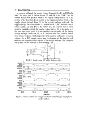
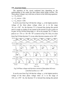
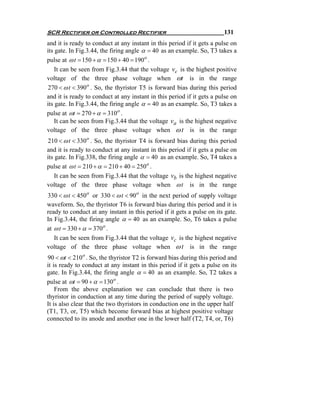
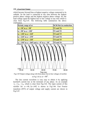
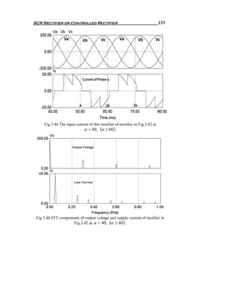
![Chapter 2
Diode Circuits or Uncontrolled Rectifier
2.1 Introduction
The only way to turn on the diode is when its anode voltage becomes
higher than cathode voltage as explained in the previous chapter. So,
there is no control on the conduction time of the diode which is the main
disadvantage of the diode circuits. Despite of this disadvantage, the diode
circuits still in use due to it’s the simplicity, low price, ruggedness,
….etc.
Because of their ability to conduct current in one direction, diodes are
used in rectifier circuits. The definition of rectification process is “ the
process of converting the alternating voltages and currents to direct
currents and the device is known as rectifier” It is extensively used in
charging batteries; supply DC motors, electrochemical processes and
power supply sections of industrial components.
The most famous diode rectifiers have been analyzed in the following
sections. Circuits and waveforms drawn with the help of PSIM simulation
program [1].
There are two different types of uncontrolled rectifiers or diode
rectifiers, half wave and full wave rectifiers. Full-wave rectifiers has
better performance than half wave rectifiers. But the main advantage of
half wave rectifier is its need to less number of diodes than full wave
rectifiers. The main disadvantages of half wave rectifier are:
1- High ripple factor,
2- Low rectification efficiency,
3- Low transformer utilization factor, and,
4- DC saturation of transformer secondary winding.
2.2 Performance Parameters
In most rectifier applications, the power input is sine-wave voltage
provided by the electric utility that is converted to a DC voltage and AC
components. The AC components are undesirable and must be kept away
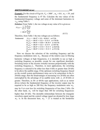
from the load. Filter circuits or any other harmonic reduction technique
should be installed between the electric utility and the rectifier and](https://image.slidesharecdn.com/powerelectronicsnote-121011031400-phpapp02/85/Power-electronics-note-25-320.jpg)
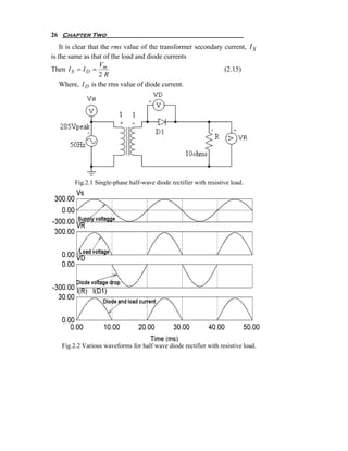

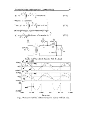
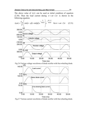
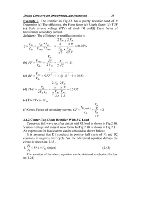
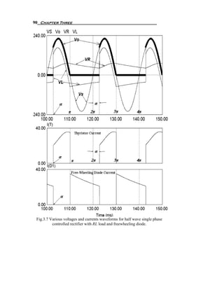
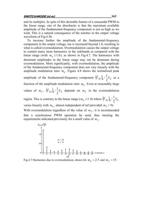
![Diode Circuits or Uncontrolled Rectifier 35
Solution: (a) For the period of 0 < ωt < π , the expression of the load
current can be obtained from (2.24) as following:
−3
−1 ωL −1 314 * 20 *10
φ = tan = tan = 0.561 rad . and tan φ = 0.628343
R 10
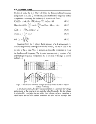
Z = R 2 + (ωL) 2 = 10 2 + (314 * 20 *10 − 3 ) 2 = 11.8084Ω
⎛ ωt ⎞
−
Vm ⎜ ⎟
i (ωt ) = sin (ωt − φ ) + sin (φ ) e tan φ
Z ⎜
⎜
⎟
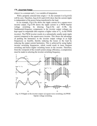
⎟
⎝ ⎠
=
220 2
11.8084
[ ]
sin (ωt − 0.561) + 0.532 * e −1.5915 ωt
i (ωt ) = 26.3479 sin (ωt − 0.561) + 14.0171* e −1.5915 ωt
The value of β can be obtained from the above equation by substituting
for i ( β ) = 0 . Then, 0 = 26.3479 sin (β − 0.561) + 14.0171 * e −1.5915 β
By using the numerical analysis we can get the value of β. The
simplest method is by using the simple iteration technique by assuming
Δ = 26.3479 sin (β − 0.561) + 14.0171 * e −1.5915 β and substitute different
values for β in the region π < β < 2π till we get the minimum value of Δ
then the corresponding value of β is the required value. The narrow
intervals mean an accurate values of β . The following table shows the
relation between β and Δ:
β Δ
1.1 π 6.49518
1.12 π 4.87278
1.14 π 3.23186
1.16 π 1.57885
1.18 π -0.079808
1.2 π -1.73761
It is clear from the above table that β ≅ 1.18 π rad. The current in
β < wt < 2π will be zero due to the diode will block the negative current
to flow.
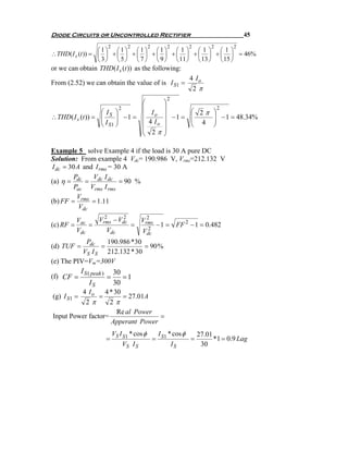
(b) In case of free-wheeling diode as shown in Fig.2.5, we have to divide
the operation of this circuit into three parts. The first one when](https://image.slidesharecdn.com/powerelectronicsnote-121011031400-phpapp02/85/Power-electronics-note-38-320.jpg)

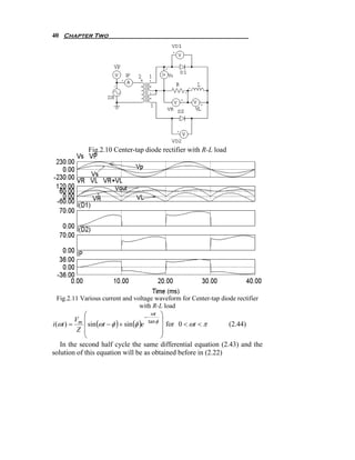

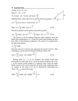
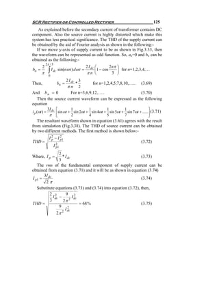
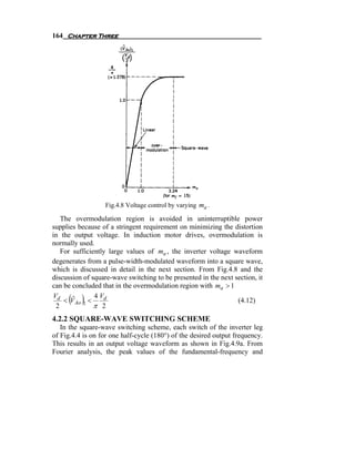
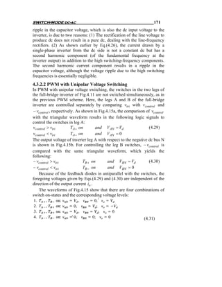
![44 Chapter Two
Fig.2.14 Full bridge single-phase diode rectifier with DC load current.
Fig.2.15 Various current and voltage waveforms for full bridge single-phase
diode rectifier with DC load current.
The supply current in case of pure DC load current is shown in
Fig.2.15, as we see it is odd function, then an coefficients of Fourier
series equal zero, an = 0 , and
π
2 2 Io
[− cos nωt ]π
π∫
bn = I o * sin nωt dωt =
nπ 0
(2.51)
0
=
2 Io
[cos 0 − cos nπ ] = 4 I o for n = 1, 3, 5, .............
nπ nπ
Then from Fourier series concepts we can say:
4 Io 1 1 1 1
i (t ) = * (sin ωt + sin 3ωt + sin 5ωt + sin 7ωt + sin 9ωt + ..........) (2.52)
π 3 5 7 9](https://image.slidesharecdn.com/powerelectronicsnote-121011031400-phpapp02/85/Power-electronics-note-47-320.jpg)
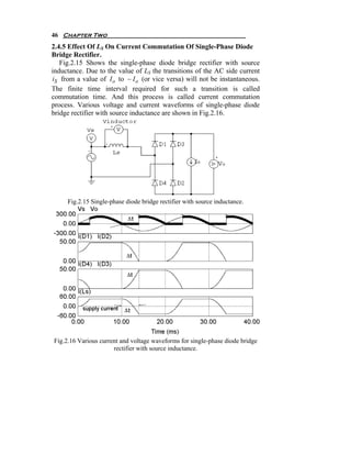
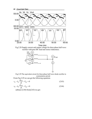
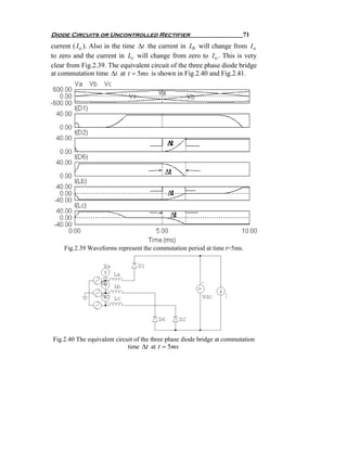
![Diode Circuits or Uncontrolled Rectifier 47
Let us study the commutation time starts at t=10 ms as indicated in
Fig.2.16. At this time the supply voltage starts to be negative, so diodes
D1 and D2 have to switch OFF and diodes D3 and D4 have to switch ON
as explained in the previous case without source inductance. But due to
the source inductance it will prevent that to happen instantaneously. So, it
will take time Δt to completely turn OFF D1 and D2 and to make D3 and
D4 carry the entire load current ( I o ). Also in the time Δt the supply
current will change from I o to − I o which is very clear in Fig.2.16.
Fig.2.17 shows the equivalent circuit of the diode bridge at time Δt .
Fig.2.17 The equivalent circuit of the diode bridge at commutation time Δt .
From Fig.2.17 we can get the following equations
di
VS − Ls S = 0 (2.53)
dt
Multiply the above equation by dωt then,
VS dωt = ωLs diS (2.54)
Integrate both sides of the above equation during the commutation
period ( Δt sec or u rad.) we get the following:
VS dωt = ωLs diS
π +u −Io
∫ Vm sin ωt dωt = ωLs ∫ diS (2.55)
π Io
Then; Vm [cos π − cos(π + u )] = −2ωLs I o
Then; Vm [− 1 + cos(u )] = −2ωLs I o](https://image.slidesharecdn.com/powerelectronicsnote-121011031400-phpapp02/85/Power-electronics-note-50-320.jpg)
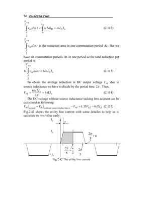
![Diode Circuits or Uncontrolled Rectifier 49
Fig. 2.18 The old axis and new axis for supply currents.
Fig.2.19 shows a symple drawing for the supply current. This drawing
help us in getting the rms valuof the supply current. It is clear from the
waveform of supply current shown in Fig.2.19 that we obtain the rms
value for only a quarter of the waveform because all for quarter will be
the same when we squaret the waveform as shown in the following
equation:
π
u/2 2 2
2 ⎛ 2I o ⎞
Is = ∫ ωt ⎟ dωt + ∫ I o dωt ]
2
[ ⎜ (2.63)
π 0 ⎝ u ⎠ u/2
2I o ⎡ 4 u 3 π u ⎤
2
2I o ⎡π u ⎤
2
Then; I s = ⎢ + − ⎥= − (2.64)
π ⎢ 3u 2 8 2 2 ⎥
⎣ ⎦ π ⎢ 2 3⎥
⎣ ⎦
Is
u
Io
π 2π
u
−
u π+
2 2
π
u 2 u
u 2π −
2
− Io π− 2
2
Fig.2.19 Supply current waveform](https://image.slidesharecdn.com/powerelectronicsnote-121011031400-phpapp02/85/Power-electronics-note-52-320.jpg)
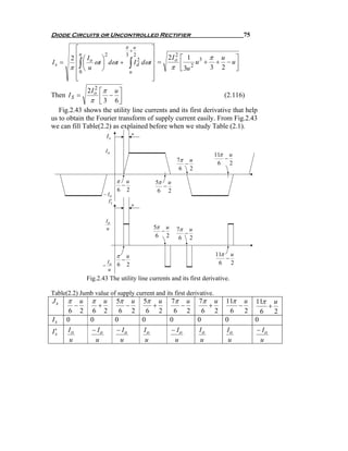
![50 Chapter Two
To obtain the Fourier transform for the supply current waveform you
can go with the classic fourier technique. But there is a nice and easy
method to obtain Fourier transform of such complcated waveform known
as jump technique [ ]. In this technique we have to draw the wave form
and its drevatives till the last drivative values all zeros. Then record the
jump value and its place for each drivative in a table like the table shown
below. Then; substitute the table values in (2.65) as following:
Is
u
Io
π 2π
u u
−
u π+
2 2 2
u u
π− 2π −
2 2
− Io
′
Is
2Io
u
π
u u
−
u π+
2 2 2
u u
π− 2π −
2I o 2 2
−
u
Fig.2.20 Supply current and its first derivative.
Table(2.1) Jumb value of supply current and its first derivative.
Js u u u u
− π− π+
2 2 2 2
Is 0 0 0 0
′
Is 2Io
−
2I o
−
2Io 2I o
u u u u](https://image.slidesharecdn.com/powerelectronicsnote-121011031400-phpapp02/85/Power-electronics-note-53-320.jpg)
![56 Chapter Two
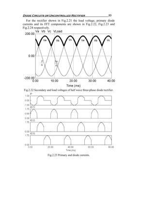
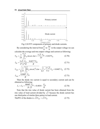
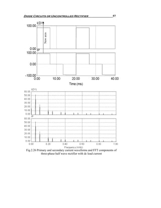
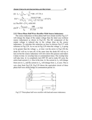
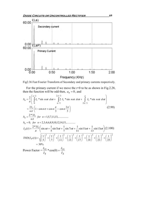
2.5.2 Three-Phase Half Wave Rectifier With DC Load Current and
zero source inductance
In case of pure DC load current as shown in Fig.2.25, the diode current
and primary current are shown in Fig.2.26.
Fig.2.25 Three-phase half wave rectifier with dc load current
To calculate Fourier transform of the diode current of Fig.2.26, it is
better to move y axis to make the function as odd or even to cancel one
coefficient an or bn respectively. If we put Y-axis at point ωt = 30o then
we can deal with the secondary current as even functions. Then, bn = 0 of
secondary current. Values of an can be calculated as following:
π /3
1 I
a0 =
2π ∫ I o dωt = 3o (2.76)
−π / 3
π /3
1
an =
π ∫ I o * cos nωt dwt
−π / 3
= o [sin nωt ]−π //3
I
π 3
nπ
I
= o * 3 for n = 1,2,7,8,13,14,.... (2.77)
nπ
I
= − o * 3 for n = 4,5,10,11,16,17
nπ
= 0 for all treplean harmonics
IO 3I O ⎛ 1 1 1 1 1 ⎞
I s (t ) = + ⎜ sin ωt + sin 2ωt − sin 4ωt − sin 5ωt + sin 7ωt + sin 8ωt − −... ⎟ (2.78)
3 π ⎝ 2 4 5 7 8 ⎠](https://image.slidesharecdn.com/powerelectronicsnote-121011031400-phpapp02/85/Power-electronics-note-59-320.jpg)
![58 Chapter Two
2
⎛ ⎞
2 ⎜ ⎟
⎛I ⎞ ⎜ Io / 3 ⎟ 2 *π 2
THD( I s (t )) = ⎜ S ⎟
⎜I ⎟ −1 = ⎜ −1 = − 1 = 1.0924 = 109.24%
⎝ S1 ⎠ ⎜ 3I O ⎟
⎟
9
⎜ π 2 ⎟
⎝ ⎠
It is clear that the primary current shown in Fig.2.26 is odd, then, an=0,
2π / 3
bn =
2
∫ I o * sin nωt dωt =
2I o
[− cos nωt ] 20π / 3
π nπ
0
3I o
= for n = 1,2,4,5,7,8,10,11,13,14,.... (2.79)
nπ
= 0 for all treplean harmonics
3I O ⎛ 1 1 1 1 1 ⎞
iP (t ) = ⎜ sin ωt + sin 2ωt + sin 4ωt + sin 5ωt + sin 7ωt + sin 8ωt − −... ⎟ (2.80)
π ⎝ 2 4 5 7 8 ⎠
2
The rms value of I P = Io (2.81)
3
2
⎛ 2 ⎞
2 ⎜ Io ⎟ 2
⎛I ⎞ 3 ⎟ − 1 = ⎛ 2π ⎞ − 1 = 67.983% (2.82)
THD ( I P (t )) = ⎜ P ⎟
⎜I ⎟ −1 = ⎜ ⎜ ⎟
⎜ 3I O ⎟ ⎝3 3⎠
⎝ P1 ⎠ ⎜ ⎟
⎝ π 2 ⎠
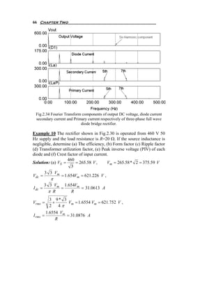
Example 8 Solve example 7 if the load current is 100 A pure DC
460
Solution: (a) VS = = 265.58 V , Vm = 265.58 * 2 = 375.59 V
3
3 3 Vm
Vdc = = 0.827 Vm = 310.613V , I dc = 100 A
2π
Vrms = 0.8407 Vm = 315.759 V , I rms = 100 A
P V I 310.613 * 100
η = dc = dc dc = = 98.37 %
Pac Vrms I rms 315.759 *100
V
(b) FF = rms = 101.657 %
Vdc
Vac Vrms − Vdc
2 2 2
Vrms
(c) RF = = = 2
− 1 = FF 2 − 1 = 18.28 %
Vdc Vdc Vdc](https://image.slidesharecdn.com/powerelectronicsnote-121011031400-phpapp02/85/Power-electronics-note-61-320.jpg)
![Diode Circuits or Uncontrolled Rectifier 67
Pdc V I
η= = dc dc = 99.83 %
Pac Vrms I rms
V
(b) FF = rms = 100.08 %
Vdc
Vac Vrms − Vdc
2 2 2
Vrms
(c) RF = = = 2
− 1 = FF 2 − 1 = 4 %
Vdc Vdc Vdc
2 1.6554 Vm V
(d) I S = I rms = 0.8165 * = 1.352 m
3 R R
Pdc (1.654Vm ) 2 / R
TUF = = = 95.42 %
3 * VS I S V
3 * Vm / 2 *1.352 m
R
(e) The PIV= 3 Vm=650.54V
I 3 Vm / R
(f) CF = S ( peak ) = = 1.281
IS Vm
1.352
R
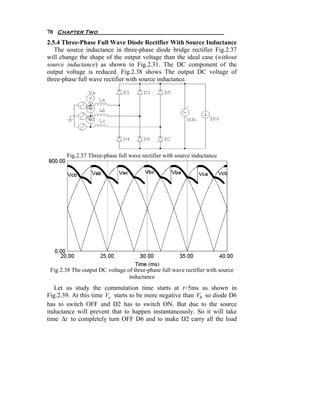
2.5.2 Three-Phase Full Wave Rectifier With DC Load Current
The supply current in case of pure DC load current is shown in
Fig.2.35. Fast Fourier Transform of Secondary and primary currents
respectively is shown in Fig2.36.
As we see it is odd function, then an=0, and
5π / 6
2
bn =
π ∫ I o * sin nωt dωt
π /6
=
2 Io
[− cos nωt ]ππ/ 66
5 /
nπ
2 Io 2 Io 2 Io
b1 = 3, b5 = (− 3 ), b7 = (− 3 ) (2.97)
π 5π 7π
2 Io 2 Io
b11 = ( 3 ), b13 = ( 3 ),.............
11π 13π
bn = 0, for n = 2,3,4,6,8,9,10,12,14,15,.............
2 3I o ⎛ 1 1 1 1 ⎞
I s (t ) = ⎜ sin ωt − sin 5v ωt − sin 7ωt + sin 11ωt + sin 13ωt ⎟ (2.98)
π ⎝ 5 7 11 13 ⎠](https://image.slidesharecdn.com/powerelectronicsnote-121011031400-phpapp02/85/Power-electronics-note-70-320.jpg)
![Diode Circuits or Uncontrolled Rectifier 73
π / 2+u
⎛ ⎛ 2π ⎞ ⎛ 2π ⎞ ⎞
∫ ⎜Vm sin ⎜ ω t − ⎟ − Vm sin ⎜ ω t + ⎟ ⎟dω t + ωLb (− I o ) − ωLc I o = 0
π /2 ⎝ ⎝ 3 ⎠ ⎝ 3 ⎠⎠
assume Lb = Lc = LS
π / 2+u
⎡ ⎛ 2π ⎞ ⎛ 2π ⎞⎤
Vm ⎢− cos⎜ ω t − ⎟ + cos⎜ ω t + ⎟ = 2ω LS I o
⎣ ⎝ 3 ⎠ ⎝ 3 ⎠⎥π / 2
⎦
⎡ ⎛π 2π ⎞ ⎛π 2π ⎞ ⎛ π 2π ⎞ ⎛ π 2π ⎞ ⎤
Vm ⎢− cos⎜ + u − ⎟ + cos⎜ + u + ⎟ + cos⎜ − ⎟ − cos⎜ + ⎟
⎣ ⎝2 3 ⎠ ⎝2 3 ⎠ ⎝2 3 ⎠ ⎝2 3 ⎠⎥⎦
= 2ω LS I o
⎡ ⎛ π⎞ ⎛ 7π ⎞ ⎛ −π ⎞ ⎛ 7π ⎞⎤
Vm ⎢− cos⎜ u − ⎟ + cos⎜ u + ⎟ + cos⎜ ⎟ − cos⎜ ⎟⎥ = 2ω LS I o
⎣ ⎝ 6⎠ ⎝ 6 ⎠ ⎝ 6 ⎠ ⎝ 6 ⎠⎦
⎡ ⎛π ⎞ ⎛π ⎞ ⎛ 7π ⎞ ⎛ 7π ⎞ 3⎤
⎢− cos(u ) cos⎜ ⎟ − sin (u ) sin ⎜ ⎟ + cos(u ) cos⎜ ⎟ − sin (u ) sin ⎜
3
⎟+ + ⎥
⎣ ⎝6⎠ ⎝6⎠ ⎝ 6 ⎠ ⎝ 6 ⎠ 2 2 ⎦
2ω LS I o
=
Vm
⎡ ⎤ 2ω LS I o
cos(u ) − 0.5 sin (u ) − cos(u ) + 0.5 sin (u ) + 3 ⎥ =
3 3
⎢−
⎣ 2 2 ⎦ Vm
2ω LS I o
3[1 − cos(u )] =
Vm
2ω LI o 2ω LI o 2 ω LS I o
cos(u ) = 1 − =1− =1−
3 Vm 2 VLL VLL
⎡ 2ω LS I o ⎤
u = cos −1 ⎢1 − ⎥ (2.109)
⎣ VLL ⎦
u 1 ⎡ 2ω LS I o ⎤
Δt = = cos −1 ⎢1 − ⎥ (2.110)
ω ω ⎣ VLL ⎦
It is clear that the DC voltage reduction due to the source inductance is
the drop across the source inductance.
di
vrd = LS D (2.111)
dt
Multiply (2.111) by dωt and integrate both sides of the resultant
equation we get:](https://image.slidesharecdn.com/powerelectronicsnote-121011031400-phpapp02/85/Power-electronics-note-76-320.jpg)
![SCR Rectifier or Controlled Rectifier 81
controller rectifiers and cycloconverters. In case of DC circuits, this
technique does not work as the DC current is unidirectional and does not
change its direction. Thus the reverse polarity voltage does not appear
across the thyristor. The following technique work with DC circuits:
2- Forced Commutation
In DC thyristor circuits, if the input voltage is DC, the forward current of
the thyristor is forced to zero by an additional circuit called commutation
circuit to turn off the thyristor. This technique is called forced
commutation. Normally this method for turning off the thyristor is
applied in choppers.
There are many thyristor circuits we can not present all of them. In the
following items we are going to present and analyze the most famous
thyristor circuits. By studying the following circuits you will be able to
analyze any other circuit.
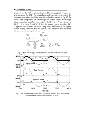
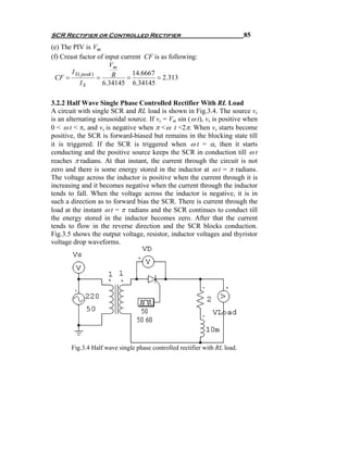
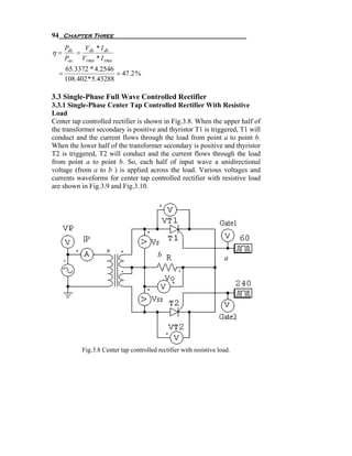
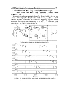
3.2 Half Wave Single Phase Controlled Rectifier
3.2.1 Half Wave Single Phase Controlled Rectifier With Resistive
Load
The circuit with single SCR is similar to the single diode circuit, the
difference being that an SCR is used in place of the diode. Most of the
power electronic applications operate at a relative high voltage and in
such cases; the voltage drop across the SCR tends to be small. It is quite
often justifiable to assume that the conduction drop across the SCR is
zero when the circuit is analyzed. It is also justifiable to assume that the
current through the SCR is zero when it is not conducting. It is known
that the SCR can block conduction in either direction. The explanation
and the analysis presented below are based on the ideal SCR model. All
simulation carried out by using PSIM computer simulation program [ ].
A circuit with a single SCR and resistive load is shown in Fig.3.1. The
source vs is an alternating sinusoidal source. If vs = Vm sin (ωt ) , vs is
positive when 0 < ω t < π, and vs is negative when π < ω t <2π. When vs
starts become positive, the SCR is forward-biased but remains in the
blocking state till it is triggered. If the SCR is triggered at ω t = α, then α
is called the firing angle. When the SCR is triggered in the forward-bias
state, it starts conducting and the positive source keeps the SCR in
conduction till ω t reaches π radians. At that instant, the current through
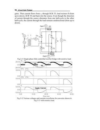
the circuit is zero. After that the current tends to flow in the reverse](https://image.slidesharecdn.com/powerelectronicsnote-121011031400-phpapp02/85/Power-electronics-note-87-320.jpg)
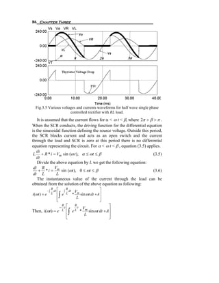
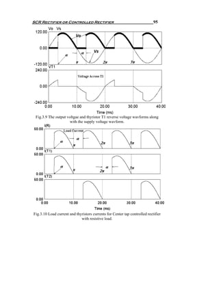
![SCR Rectifier or Controlled Rectifier 99
Fig.3.13 FFT components of the output voltage and supply current for converter
shown in Fig.3.11.
The main purpose of this circuit is to provide a controllable DC output
voltage, which is brought about by varying the firing angle, α. Let vs = Vm
sin ω t, with 0 < ω t < 360o. If ω t = 30o when T1 and T2 are triggered,
then the firing angle α is said to be 30o. In this instance, the other pair is
triggered when ω t = 30+180=210o. When vs changes from positive to
negative value, the current through the load becomes zero at the instant
ω t = π radians, since the load is purely resistive. After that there is no
current flow till the other is triggered. The conduction through the load is
discontinuous.
The average value of the output voltage is obtained as follows.:-
Let the supply voltage be vs = Vm*Sin ( ω t), where ω t varies from 0 to
2π radians. Since the output waveform repeats itself every half-cycle, the
average output voltage is expressed as a function of α, as shown in
equation (3.27).
π
1 Vm
[− cos π − (− cos(α ) )] = Vm (1 + cosα ) (3.27)
π∫ m
Vdc = V sin(ω t ) dω t =
π π
α
Vdm is the maximum output voltage and can be acheaved when α=0,
The normalized output voltage is:
Vdc
Vn = = 0.5 (1 + cos α ) (3.28)
Vdm
The rms value of output voltage is obtained as shown in equation (3.29).
π
Vm sin(2 α )
1
(V sin(ω t ) )
π∫ m
Vrms = 2
dω t = π −α + (3.29)
α
2π 2](https://image.slidesharecdn.com/powerelectronicsnote-121011031400-phpapp02/85/Power-electronics-note-105-320.jpg)
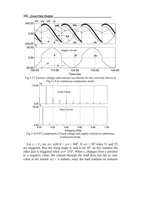
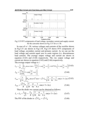
![SCR Rectifier or Controlled Rectifier 109
Let us study the commutation period starts at α < ω t < α + u . When
T1 and T2 triggered, then T1 and T2 switched on and T3 and T4 try to
switch off. If this happens, the current in the source inductance has to
change its direction. But source inductance prevents that to happen
instantaneously. So, it will take time Δt to completely turn off T3 and T4
and to make T1 and T2 carry the entire load current I o which is very
clear from Fig.3.20. Also, in the same time ( Δt ) the supply current
changes from − I o to I o which is very clear from Fig.3.21. Fig.3.22
shows the equivalent circuit of the single phase full-wave controlled
rectifier during that commutation period. From Fig.3.22 We can get the
differential equation representing the circuit during the commutation time
as shown in (3.41).
Fig.3.22 The equivalent circuit of single phase fully controlled rectifier
during the commutation period.
dis
v s − Ls =0 (3.41)
dt
Multiply the above equation by ωt then,
Vm sin ω t dωt − ω Ls dis = 0
Integrate the above equation during the commutation period we get the
following:
α +u Io
∫Vm sin ω t dω t = ω Ls ∫ dis
α −Io
Then, Vm [cos α − cos(α + u )] = 2ωLs I o . Then,
2ωLs I o
cos(α + u ) = cos α −
Vm](https://image.slidesharecdn.com/powerelectronicsnote-121011031400-phpapp02/85/Power-electronics-note-115-320.jpg)
![112 Chapter Three
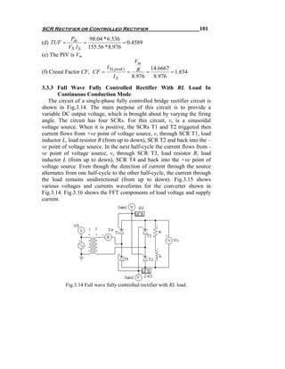
Fig.3.23 Single-phase half controlled bridge rectifier (semi bridge converter).
π
1 Vm
[− cos π − (− cos(α ))] = Vm (1 + cosα ) (3.52)
π∫ m
Vdc = V sin(ω t ) dω t =
π π
α
Vdm is the maximum output voltage and can be acheaved when α=0,
V
The normalized output voltage is: Vn = dc = 0.5 (1 + cos α ) (3.53)
Vdm
The rms value of output voltage is obtained as shown in the following
equation:-
π
Vm sin(2 α )
1
(Vm sin(ω t ) )
π∫
Vrms = 2
dω t = π −α + (3.54)
α
2π 2
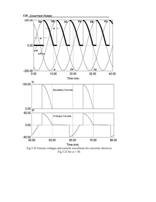
Fig.3.24 Various voltages and currents waveforms for the converter shown in Fig.3.23.](https://image.slidesharecdn.com/powerelectronicsnote-121011031400-phpapp02/85/Power-electronics-note-118-320.jpg)

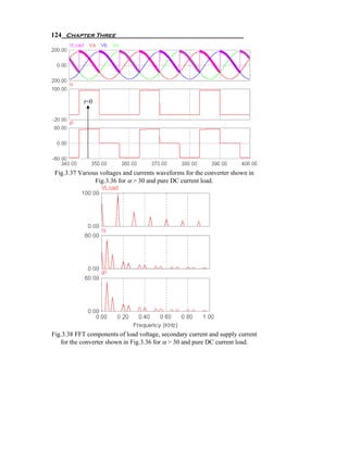

π 6 π
π / 6 +α
The maximum average output voltage for delay angle α=0 is
3 3 Vm
Vdm = (3.86)
π
The normalized average output voltage is
Vn = dc = [1 + cos ( π / 3 + α )]
V
(3.87)
Vdm
The rms value of the output voltage is found from the following
equation:
5π / 6 2
3 ⎛ π ⎞
Vrms =
π ⎝∫
3 ⎜Vm sin(ω t + ) ⎟ dω t
6 ⎠
π / 6 +α (3.88)
3 ⎛ ⎛ π ⎞⎞
= 3Vm 1 − ⎜ 2α − cos⎜ 2α + ⎟ ⎟
4π ⎝ ⎝ 6 ⎠⎠
Example 10 Three-phase full-wave controlled rectifier is connected to
380 V, 50 Hz supply to feed a load of 10 Ω pure resistance. If it is
required to get 400 V DC output voltage, calculate the following: (a) The
firing angle, α (b) The rectfication effeciency (c) The crest factor of
input current. (d) PIV of the thyristors.
Solution: From (3.81) the average voltage is :
2
3 3* * 380
3 3 Vm 3
Vdc = cos α = cos α = 400V .
π π
Vdc 400
Then α = 38.79 o , = I dc =
= 40 A
R 10
From (3.84) the rms value of the output voltage is:
⎛1 3 3 ⎞ 2 ⎛1 3 3 ⎞
Vrms = 3 Vm ⎜ ⎟
⎜ 2 + 4 π cos 2 α ⎟ = 3 * 3 * 380 *
⎜ +
⎜2 cos (2 * 38.79 )⎟
⎟
⎝ ⎠ ⎝ 4π ⎠
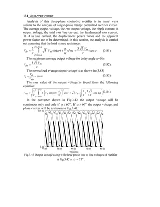
Then, Vrms = 412.412 V](https://image.slidesharecdn.com/powerelectronicsnote-121011031400-phpapp02/85/Power-electronics-note-141-320.jpg)
![136 Chapter Three
Vrms 412.412
Then, I rms = = = 41.24 A
R 10
V *I 400 * 40
Then, η = dc dc *100 = *100 = 94.07%
Vrms * I rms 412.4 * 41.24
I S , peak
The crest factor of input current, C F =
I s, rms
⎛ π⎞
2 * 380 sin ⎜ ωt + ⎟
⎝ 6⎠ 2 * 380 sin (30 + 38.79 + 30)
I S , peak = = = 53.11 A
R 10
2 2
I s , rms = *I rms = * 41.24 = 33.67 A
3 3
I S , peak 53.11
Then, C F = = = 1.577
I s, rms 33.67
The PIV= 3 Vm=537.4V
Example 11 Solve the previous example if the required dc voltage is 150V.
Solution: From (3.81) the average voltage is :
2
3 3* * 380
3 3 Vm 3
Vdc = cos α = cos α = 150V . Then, α = 73o
π π
It is not acceptable result because the above equation valid only for
α ≤ 60 . Then we have to use the (3.85) to get Vdc as following:
2
3 3* * 380
Vdc == 3 [1 + cos ( π / 3 + α )] = 150V . Then, α = 75.05o
π
V 150
Then I dc = dc = = 15 A
R 10
From (3.88) the rms value of the output voltage is:
3 ⎛ ⎛ π ⎞⎞
Vrms = 3Vm 1 − ⎜ 2α − cos⎜ 2α + ⎟ ⎟
⎜
4π ⎝ ⎝ 6 ⎠⎟
⎠
2 ⎛ 3 ⎛ π ⎞⎞
= 3* * 380 * ⎜ 4 π ⎜ 2 * 75.05 * 180 − cos (2 * 75.05 + 30 )⎟ ⎟
⎜1 − ⎟
3 ⎝ ⎝ ⎠⎠](https://image.slidesharecdn.com/powerelectronicsnote-121011031400-phpapp02/85/Power-electronics-note-142-320.jpg)
![144 Chapter Three
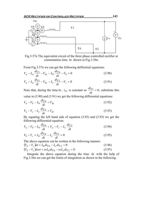
π / 2 +α + u 0 Io
∫ (Vb − Vc )dω t + ∫ ω Lb diT 6 − ∫ ω Lc diT 2 = 0
π / 2 +α Io 0
π / 2 +α + u
⎛ ⎛ 2π ⎞ ⎛ 2π ⎞ ⎞
∫ ⎜Vm sin ⎜ ω t − ⎟ − Vm sin ⎜ ω t + ⎟ ⎟dω t + ωLb (− I o ) − ωLc I o = 0
π / 2 +α ⎝ ⎝ 3 ⎠ ⎝ 3 ⎠⎠
assume Lb = Lc = LS
π / 2 +α + u
⎡ ⎛ 2π ⎞ ⎛ 2π ⎞⎤
Vm ⎢− cos⎜ ω t − ⎟ + cos⎜ ω t + ⎟ = 2ω LS I o
⎣ ⎝ 3 ⎠ ⎝ 3 ⎠⎥ π / 2 +α
⎦
⎡ ⎛π 2π ⎞ ⎛π 2π ⎞ ⎛π 2π ⎞ ⎛π 2π ⎞⎤
Vm ⎢− cos⎜ + α + u − ⎟ + cos⎜ + α + u + ⎟ + cos⎜ + α − ⎟ − cos⎜ + α + ⎟⎥
⎣ ⎝2 3 ⎠ ⎝2 3 ⎠ ⎝2 3 ⎠ ⎝2 3 ⎠⎦
= 2ω LS I o
⎡ ⎛ π⎞ ⎛ 7π ⎞ ⎛ π⎞ ⎛ 7π ⎞⎤
Vm ⎢− cos⎜ α + u − ⎟ + cos⎜ α + u + ⎟ + cos⎜ α − ⎟ − cos⎜ α + ⎟⎥ = 2ω LS I o
⎣ ⎝ 6⎠ ⎝ 6 ⎠ ⎝ 6⎠ ⎝ 6 ⎠⎦
⎡ ⎛π ⎞ ⎛π ⎞ ⎛ 7π ⎞ ⎛ 7π ⎞
⎢− cos(α + u )cos⎜ 6 ⎟ − sin (α + u )sin ⎜ 6 ⎟ + cos(α + u )cos⎜ 6 ⎟ − sin (α + u )sin ⎜ 6 ⎟
⎣ ⎝ ⎠ ⎝ ⎠ ⎝ ⎠ ⎝ ⎠
π π 7π 7π ⎤ 2ω LS I o
+ cos α cos + sin α sin − cos α cos + sin α sin ⎥ =
6 6 6 6 ⎦ Vm
⎡ 3
cos(α + u ) − 0.5 sin (α + u ) − cos(α + u ) + 0.5 sin (α + u )
3
⎢−
⎣ 2 2
3 3 ⎤ 2ω LS I o
cos α + 0.5 sin α cos α − 0.5 sin α ⎥ =
2 2 ⎦ Vm
2ω LS I o
3[cos α − cos(α + u )] =
Vm
2ω LI o 2ω LI o 2 ω LS I o
cos(α ) − cos(α + u ) = = = (3.98)
3 Vm 2 VLL VLL
⎡ 2ω LS I o ⎤
u = cos −1 ⎢cos(α ) − ⎥ −α (3.99)
⎣ VLL ⎦
u 1⎧ ⎪ ⎡ 2ω LS I o ⎤ ⎫
⎪
Δt = = ⎨cos −1 ⎢cos(α ) − ⎥ −α ⎬ (3.100)
ω ω⎪ ⎩ ⎣ VLL ⎦ ⎪
⎭](https://image.slidesharecdn.com/powerelectronicsnote-121011031400-phpapp02/85/Power-electronics-note-150-320.jpg)
![148 Chapter Three
Note, if we approximate the source current to be trapezoidal as shown in
Fig.3.58n, the displacement power factor will be as shown in (3.111) is
⎛ u⎞
cos⎜ α + ⎟ . Another expression for the displacement power factor, by
⎝ 2⎠
equating the AC side and DC side powers [ ] as shown in the following
derivation:
From (3.98) and (3.105) we can get the following equation:
VLL (cosα − cos(α + u ))
3 2 3
Vdc = VLL cos α −
π 2π
VLL [2 cos α − (cos α − cos(α + u ))]
3 2
∴Vdc =
2π
VLL [cos α + cos(α + u )]
3 2
∴Vdc = (3.112)
2π
Then the DC power output from the rectifier is Pdc = Vdc I o . Then,
VLL * I o [cos α + cos(α + u )]
3 2
Pdc = (3.113)
2π
On the AC side, the AC power is:
Pac = 3 VLL I S1 cos φ1 (3.114)
Substitute from (3.110) into (3.114) we get the following equation:
4 3 Io ⎛ u ⎞ 6 2 VLL I o ⎛ u ⎞
Pac = 3 VLL sin ⎜ ⎟ cos φ1 = sin ⎜ ⎟ cos φ1 (3.115)
πu 2 ⎝2⎠ πu ⎝2⎠
By equating (3.113) and (3.115) we get the following:
u [cos α + cos (α + u )]
cos φ1 = (2.116)
⎛u⎞
4 * sin ⎜ ⎟
⎝2⎠
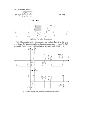
The source inductance reduces the magnitudes of the harmonic
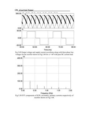
currents. Fig.3.60a through d show the effects of LS (and hence of u) on
various harmonics for various values of α , where I d is a constant dc.
The harmonic currents are normalized by I1 I, with LS = 0 , which is
6
given by (2.98) where I s1 = I o in this case. Normally, the DC-side
π
current is not a constant DC. Typical and idealized harmonics are shown
in Table 3.2.](https://image.slidesharecdn.com/powerelectronicsnote-121011031400-phpapp02/85/Power-electronics-note-154-320.jpg)
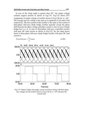
![SCR Rectifier or Controlled Rectifier 149
Fig.3.60 Normalized harmonic current in the presence of LS [ ].
Table 3.2 Typical and idealized harmonics.
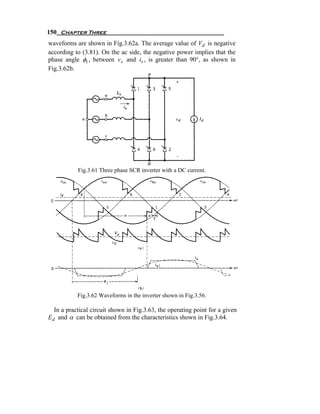
3.7.2 Inverter Mode of Operation
Once again, to understand the inverter mode of operation, we will
assume that the do side of the converter can be represented by a current
source of a constant amplitude I d , as shown in Fig.3.61. For a delay
angle a greater than 90° but less than 180°, the voltage and current](https://image.slidesharecdn.com/powerelectronicsnote-121011031400-phpapp02/85/Power-electronics-note-155-320.jpg)


![194 Chapter Three
A careful examination shows that the switching frequency of a switch
in Fig.4.38 is seven times the switching frequency associated with a
square-wave operation.
In a square-wave operation, the fundamental-frequency voltage
component is:
( )
ˆ
V Ao 1 4
= = 1.273 (4.73)
Vd / 2 π
Because of the notches to eliminate 5th and 7th harmonics, the maximum
available fundamental amplitude is reduced. It can be shown that:
( )
ˆ
V Ao 1, max
= 1.188 (4.74)
Vd / 2
Fig.4.38 Programable harmonic elemination of fifth and seventh harmonics.
It is clear that the waveform in Fig.4.38 is odd function. So,
1 ⎡m ⎤
bn = ⎢ ∑ J s cos nωt ⎥ (4.75)
nπ ⎢ s =1
⎣ ⎥
⎦
Where m is the number of jumps in the waveform. Jumps of the
waveform shown in the figure is for only quarter of the waveform
(because of similarity). The jumps are tabulated in the following table.
Js J1 J2 J3 J4
Time 0 α1 α2 α3
Value 2 -2 2 -2
Then, bn =
2
[2 cos n0 − 2 cos nα1 + 2 cos nα 2 − 2 cos nα 3 ] (4.76)
nπ
π
Where α1 < α 2 < α 3 <
2](https://image.slidesharecdn.com/powerelectronicsnote-121011031400-phpapp02/85/Power-electronics-note-203-320.jpg)
![SWITCH-MODE dc-ac 195
The above equation has three variables α1, α 2 , and α 3 so we need
three equation to obtain them. The First equation can be obtained by
assigning a specific value to the amplitude of the fundamental component
b1 . Another two equations can be obtained by equating b5 , and b7 by
zero to eliminate fifth and seventh harmonics. So, the following equations
can be obtained.
b1 = [1 − cos α1 + cos α 2 − cos α 3 ]
4
(4.77)
π
b5 = [1 − cos 5α1 + cos 5α 2 − cos 5α 3 ] = 0
4
(4.78)
π
b7 = [1 − cos 7α1 + cos 7α 2 − cos 7α 3 ] = 0
4
(4.79)
π
The above equation can be rearranged to be in the following form:
⎡ π b1 ⎤
⎡ cos α1 − cos α 2 cos α 3 ⎤ ⎢1 −
⎢cos 5α − cos 5α 4 ⎥
⎢ cos 5α 3 ⎥ = ⎢ 1 ⎥
⎥
(4.80)
1 2
⎢ ⎥
⎣ cos α1
⎢ − cos 7α 2 cos 7α 3 ⎥
⎦ ⎢ 1 ⎥
⎢
⎣ ⎥
⎦
These equations are nonlinear having multiple solution depending the
value of b1 . Computer programs help us in solving the above equations.
The required values of α1 , α 2 , and α 3 are plotted in Fig.4.39 as a
function of the normalized fundamental in the output voltage.
Fig.4.39 The required values of α1 , α 2 , and α 3 .](https://image.slidesharecdn.com/powerelectronicsnote-121011031400-phpapp02/85/Power-electronics-note-204-320.jpg)
![196 Chapter Three
To allow control over the fundamental output and to eliminate the
fifth-, seventh-, eleventh-, and the thirteenth-order harmonics, five
notches per half-cycle would be needed. In that case, each switch would
have 11 times the switching frequency compared with a square-wave
operation.
Example Eliminate fifth and seventh harmonics from square
waveform with no control on the fundamental amplitude:
Solution: It is clear that we have only two conditions which are b5 = 0
and b7 = 0 . So, we have only two notches per half cycle as shown in the
following figure.
V Ao
Vd / 2
Notch1
Notch2 π + α1
π + α2
ω1t
α1 α2 π − α 2 π − α1
π 2π
2π − α 2 2π − α1
So we need only two variables α1 and α 2 which can be obtained from
the following equations:
bn =
4
[1 − cos nα1 + cos nα 2 ] (4.81)
nπ
b5 = [1 − cos 5α1 + cos 5α 2 ] = 0
4
(4.82)
π
b7 = [1 − cos 7α1 + cos 7α 2 ] = 0
4
(4.83)
π
⎡ cos 5α1 − cos 5α 2 ⎤ ⎡1⎤
⎢ ⎥=⎢⎥ (4.84)
⎣cos 7α1 − cos 7α 2 ⎦ ⎣1⎦
By solving the above equation we can get the value of α1 and α 2 as
following:
α1 = 12.8111o and α 2 = 24.8458o
The following table shows the absolute value of each harmonics after
eliminating fifth and seventh harmonics.](https://image.slidesharecdn.com/powerelectronicsnote-121011031400-phpapp02/85/Power-electronics-note-205-320.jpg)
![SWITCH-MODE dc-ac 197
Harmonic bn for square wave bn =
4 bn after eliminating 5th and 7th
order nπ
bn =
4
[1 − cos nα1 + cos nα 2 ]
nπ
1 1.27324 1.1871
3 0.244413 0.20511
5 0.25468 0.0
7 0.18189 0.0
9 0.14147 0.0995
11 0.11575 0.21227
13 0.09794 0.27141
15 0.08488 0.25067
17 0.07490 0.16881
19 0.06701 0.07183
21 0.06063 0.00407
THD 22.669% 26.201%
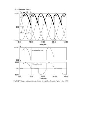
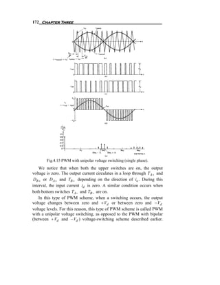
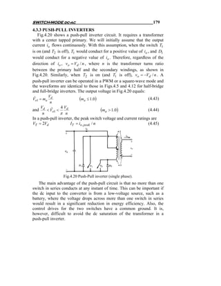
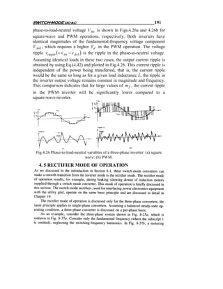
4.7 LOW COST PWM CONVERTER FOR UTILITY INTERFACE.
As discussed in regular three phase PWM inverter, the existing
configuration uses six switches as shown in Fig.4.21. The low cost PWM
inverter (Four switch inverter) uses four semiconductor switches. The
reduction in number of switches reduces switching losses, system cost and
enhances reliability of the system.
Fig.4.40 shows the proposed converter with four switches (Four
Switch Topology, FST) By comparing Fig.4.40 and Fig.4.21, it is clear
that, by using one additional capacitor one can replace two switches and
the system will perform the same function. It is apparent that the cost and
reliability are two major advantages of the proposed converter. The cost
reduction can be accomplished by reducing the number of switches and
the complexity of control system. The proposed converter current
regulated with good power quality characterization.
S3 S1
Vd
a
2 b
Vd c
2 S4 S2
Fig.4.40 Four switch converter.](https://image.slidesharecdn.com/powerelectronicsnote-121011031400-phpapp02/85/Power-electronics-note-206-320.jpg)


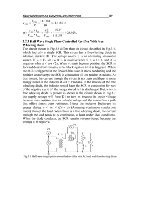
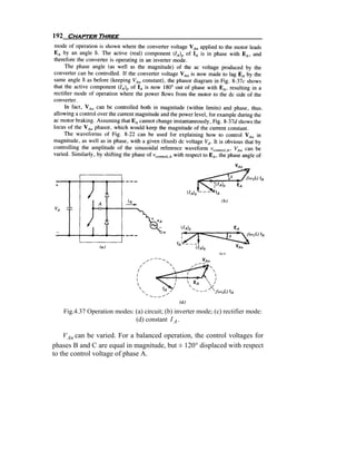
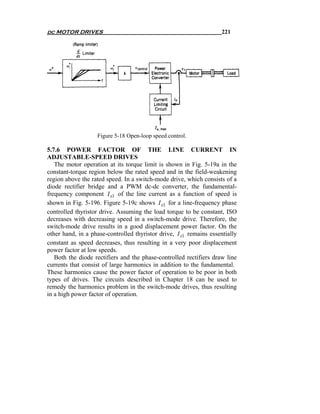
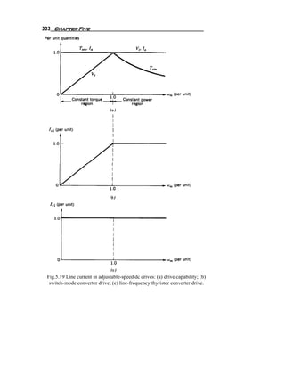
![dc MOTOR DRIVES 213
armature current can be expressed in terms of their dc and the ripple
components as
vt (t ) = Vt + vr (t ) (5.32)
ia (t ) = I a + ir (t ) (5.33)
where vr (t ) and ir (t ) are the ripple components in vt and ia ,
respectively. Therefore, in the armature circuit, from Eq. 5.8,
di (t )
Vt + vr (t ) = Ea + R A [I a + ir (t )] + La r (5.34)
dt
Where Vt = E a + Ra I a (5.35)
di (t )
And vr (t ) = Ra ir (t ) + La r (5.36)
dt
Assuming that the ripple current is primarily determined by the armature
inductance La and Ra has a negligible effect, from Eq. 5-36
di (t )
vr (t ) ≅ La r (5.37)
dt
2
The additional heating in the motor is approximately Ra I r where I r is
the rms value of the ripple current ir .
The ripple voltage is maximum when the average output voltage in a
dc is zero and all switches operate at equal duty ratios. Applying these
results to the dc motor drive, Fig. 5-11a shows the voltage ripple vr (t )
and the resulting ripple current ir (t ) using Eq. 5.37. From these
waveforms, the maximum peak-to-peak ripple can be calculated as:
V
(ΔI P − P )max = d (5.38)
2 La f s
where Vd is the input dc voltage to the full-bridge converter.](https://image.slidesharecdn.com/powerelectronicsnote-121011031400-phpapp02/85/Power-electronics-note-224-320.jpg)
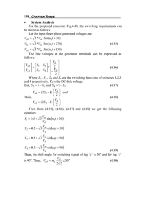
![224 Chapter Six
6.2 Harmonics analysis of the load voltage (and current)
The load voltage eL can be expressed as :-
a0 ∞ a ∞
e L (ωt ) = + ∑ a n cos nωt + bn sin nωt = 0 + ∑ C n sin(n ωt + ψ )
2 n =1 2 n =1
a0 1 2π
where, =
2 2π 0 ∫
eL (ωt ) dωt = Average value
For fundamental component :-
1 2π 1 2π
a1 = ∫ e L (ωt ) cos ωt dωt , b1 = ∫ e L (ωt ) sinωt dωt
π 0 π 0
c1 = a12 + b12 = peak value of fundamental component
a1
ψ 1 = tan −1 = displacement angle between the fundamental and
b1
the datum point.
For the n-th harmonics,
1 2π 1 2π
a n = ∫ e L (ωt ) cos nωt dωt ,
π ∫0
bn = e L (ωt ) sin nωt dωt
π 0
For the fundamental of the load voltage,
1 2π Em
π ∫0
a1 = e L (ωt ) cos ωt dωt = (cos 2α − 1)
2π
Em
b1 = (2 (π − α ) + sin 2α )
2π
E
c1 = m (cos 2α − 1) 2 + [2 (π − α ) + sin 2α ]2
2π
a cos 2α − 1
ψ 1 = tan −1 1 = tan −1
b1 2(π − α ) + sin 2α
RMS Load Voltage
1 2π
r.m.s. value of eL = E L =
2π ∫0 eL 2 (ωt ) dωt
1 π ,2π E 2
2π ∫α ,α +π
EL 2 = ( E m sin ωt ) 2 dωt = m [ 2 (π − α ) + sin 2α ]
4π
E 1
EL = m [2(π − α ) + sin 2α ]
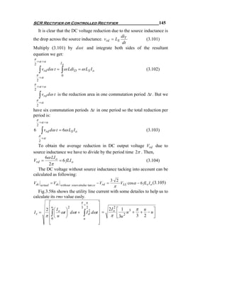
2 2π](https://image.slidesharecdn.com/powerelectronicsnote-121011031400-phpapp02/85/Power-electronics-note-237-320.jpg)
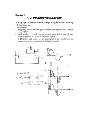
![A.C. Voltage Regulators 225
with resistive load, the instantaneous load current is :-
e E sin ωt π ,2π
iL = L = m |α ,π +α
R R
The r.m.s. load current
E 1 E 1
IL = m [ 2(π − α ) + sin 2α ] = [2(π − α ) + sin 2α ]
2 R 2π R 2π
6.3 Power Dissipation
1 2π
P=
2π 0 ∫eL i dt = Average value of instantaneous volt − amp product.
= Average power
EL 2
= I L2 R = where I L & E L are the r.m.s. values
R
E2
= [2(π − α ) + sin 2α ]
2πR
In terms of harmonic components:-
1 2
P = R ( I12 + I 32 + I 5 2 + .......) = ( E L1 + E L3 + E L5 + .......)
2 2
R
In terms of fundamental components: P = E I1 cos ψ 1
where I1 = r.m.s. fundamental current = c1 1 , cosψ 1 =
b1
2 R c1
6.4 Power factor in non-sinusoidal circuits
Average Power P
In general, PF = =
Apparent Voltamperes E I
E = r.m.s. voltage at supply.
I = r.m.s. current at supply.
Definition is true irrespective for any waveform and frequency.
Let e and i be periodic in 2π ,
1 2π
P=
2π 0 ∫
e i dωt
1 2π 2 1 2π 2
E=
2π 0 ∫
e dωt ; I =
2π 0
i dω t ∫
The usual aim is to obtain unity PF at the supply.](https://image.slidesharecdn.com/powerelectronicsnote-121011031400-phpapp02/85/Power-electronics-note-238-320.jpg)
![226 Chapter Six
To obtain unity P.F., certain conditions must be observed w.r.t. e(ω t) and
i(ωt):-
(i) e(ω t) and i(ωt) must be of the same frequency.
(ii) e(ω t) and i(ωt) must be of the same wave shape (whatever the
wave shape)
(iii) e(ω t) and i(ωt) must be in time-phase at every instant of the cycle.
Power Factor in systems with sinusoidal voltage (at supply) but non-
sinusoidal current
i (wt ) is periodic in 2π but is non-sinusoidal.
Average power is obtained by combining in-phase voltage and current
components of the same frequency.
P = E I1 cos ψ 1
P E I1 cos ψ 1 I1
PF = = = cos ψ 1
EI EI I
= Distortion Factor x Displacement Factor
Distortion Factor = 1 for sinusoidal operation
Displacement factor is a measure of displacement between e(ω t) and
i(ωt).
Displacement Factor =1 for sinusoidal resistive operation.
Calculation of PF
E2 R
[2(π − α ) + sin 2α ]
I 2R 2π R 2 1
PF = = = [2(π − α ) + sin 2α ]
EI E 1 2π
E [2(π − α ) + sin 2α ]
R 2π
R-L load
ωL
Z = R 2 + ω 2 L2 , φ = tan −1
R](https://image.slidesharecdn.com/powerelectronicsnote-121011031400-phpapp02/85/Power-electronics-note-239-320.jpg)
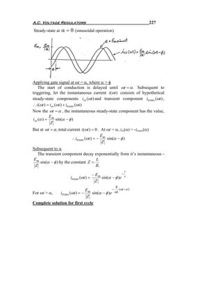
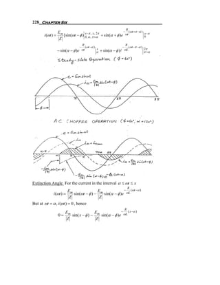
![A.C. Voltage Regulators 229
Em R
But ≠ 0 and = cot φ ∴ 0 = sin( x − φ ) − sin(α − φ )e − cot( x −α )
Z ωL
If α and φ are known, x can be calculated. However, this is a
transcendental equation (i.e. cannot be solved explicitly and no way of
obtaining x = f (α , φ ) ).
Method of solution is by iteration,
e.g. If φ = 600, α = 1200 = 2π / 3, cot φ = 0.578
2π
− 0.578( x − )
sin( x − 60 ) = sin(120 − 60)e
0 0 3 ⇒ x = 2220
Rough Approximation :- x = 180 0 + φ − Δ
Δ = 5 0 ~ 10 0 for large R and small ωL
where
= 10 0 ~ 15 0 for R = ωL = 150 ~ 20 0 for small R and large ωL
For the previous example,
φ = 60 0 , Δ = 150 − 20 0
∴ x = 180 0 + 60 0 − 15 0 = 225 0
or x = 180 0 + 60 0 − 20 0 = 220 0
Load voltage
eL (ωt ) = Em sin ωt 0,−π,π x α π
x , ,2
α +
Em
a1 = [cos 2α − cos 2 x]
2π
E
b1 = m [2( x − α ) − sin 2 x + sin 2α ]
2π](https://image.slidesharecdn.com/powerelectronicsnote-121011031400-phpapp02/85/Power-electronics-note-242-320.jpg)
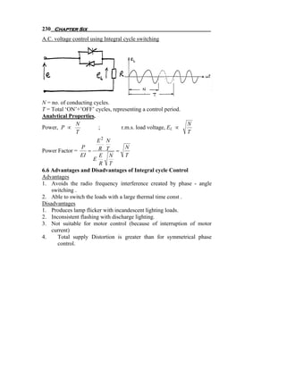


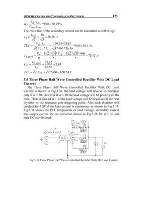
![Fundamentals of power electronics [presentation slides] 2nd ed r. erickson ww](https://cdn.slidesharecdn.com/ss_thumbnails/fundamentalsofpowerelectronicspresentationslides2nded-r-ericksonww-100522135011-phpapp02-thumbnail.jpg?width=640&height=640&fit=bounds)


