Download as PDF, PPTX
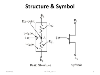
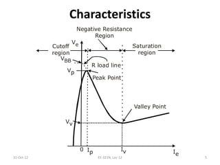

The document provides an overview of the Unijunction Transistor (UJT), describing its unique three-terminal structure and various applications including trigger circuits and oscillators. It explains the device's characteristics, operation, and how it can exhibit negative resistance, which is utilized in relaxation oscillators. Additionally, it includes information on circuit configurations, charging and discharging processes, and key parameters for design considerations.


![Multisim_simulation_project_3_^0_4[1]-2.pptx](https://cdn.slidesharecdn.com/ss_thumbnails/multisimsimulationproject3041-2-240418183400-1d9cbd89-thumbnail.jpg?width=640&height=640&fit=bounds)


