Ieee Mttv055i05 20070505th Edition Fantomasping
download
https://ebookbell.com/product/ieee-mttv055i05-200705-05th-
edition-fantomasping-30972946
Explore and download more ebooks at ebookbell.com
2.
Here are somerecommended products that we believe you will be
interested in. You can click the link to download.
Ieee Mttv051i05 200305 5th Edition Fantomasping
https://ebookbell.com/product/ieee-mttv051i05-200305-5th-edition-
fantomasping-44874560
Ieee Mttv054i05 200605 5th Edition Fantomasping
https://ebookbell.com/product/ieee-mttv054i05-200605-5th-edition-
fantomasping-28162186
Ieee Mttv053i05 200505 05th Edition Fantomasping
https://ebookbell.com/product/ieee-mttv053i05-200505-05th-edition-
fantomasping-30972978
Ieee Mttv052i05 200405 5th Edition Fantomasping
https://ebookbell.com/product/ieee-mttv052i05-200405-5th-edition-
fantomasping-7434088
MAY 2007 VOLUME55 NUMBER 5 IETMAB (ISSN 0018-9480)
PAPERS
Linear and Nonlinear Device Modeling
Pruning the Volterra Series for Behavioral Modeling of Power Amplifiers Using Physical Knowledge ....................
............................................................................................ A. Zhu, J. C. Pedro, and T. R. Cunha 813
Modeling Superconducting Transmission Line Bends and Their Impact on Nonlinear Effects ..............................
.................................................................................. J. Mateu, C. Collado, and J. M. O’Callaghan 822
Analytic Large-Signal Modeling of Silicon RF Power MOSFETs ........ P. Fioravanti, O. Spulber, and M. M. De Souza 829
Smart Antennas, Phased Arrays, and Radars
A High-Directivity Combined Self-Beam/Null-Steering Array for Secure Point-to-Point Communications ...............
.......................................... G. S. Shiroma, R. Y. Miyamoto, J. D. Roque, J. M. Cardenas, and W. A. Shiroma 838
Active Circuits, Semiconductor Devices, and ICs
Polar SiGe Class E and F Amplifiers Using Switch-Mode Supply Modulation ...............................................
......................................................................... J. N. Kitchen, I. Deligoz, S. Kiaei, and B. Bakkaloglu 845
A 23-dBm 60-GHz Distributed Active Transformer in a Silicon Process Technology ........ U. R. Pfeiffer and D. Goren 857
A Mixed-Signal Approach Towards Linear and Efficient -Way Doherty Amplifiers .......................................
.......................................... W. C. E. Neo, J. Qureshi, M. J. Pelk, J. R. Gajadharsing, and L. C. N. de Vreede 866
Signal Generation, Frequency Conversion, and Control
GaInP/GaAs HBT Sub-Harmonic Gilbert Mixers Using Stacked-LO and Leveled-LO Topologies .........................
........................................................................ T.-H. Wu, S.-C. Tseng, C.-C. Meng, and G.-W. Huang 880
Millimeter-Wave and Terahertz Technologies
Design of High-Performance Millimeter Wave and Sub-Millimeter Wave Quasi-Optical Isolators and Circulators .......
....................................................................... R. I. Hunter, D. A. Robertson, P. Goy, and G. M. Smith 890
Millimeter-Wave Transition From Waveguide to Two Microstrip Lines Using Rectangular Patch Element ................
...................................................................................... H. Iizuka, K. Sakakibara, and N. Kikuma 899
(Contents Continued on Back Cover)
6.
(Contents Continued fromFront Cover)
Wireless Communication Systems
RF Front-End Passive Circuit Implementation Including Antenna for ZigBee Applications .................................
............................... C.-S. Yoo, J.-K. Lee, D. Kim, S.-D. Park, K.-H. Won, N.-K. Kang, K.-S. Seo, and W.-S. Lee 906
Wideband Design of the Fully Integrated Transmitter Front-End With High Power-Added Efficiency .....................
............................................................................................................ H. Kim and Y. J. Yoon 916
Weighted Polynomial Digital Predistortion for Low Memory Effect Doherty Power Amplifier .............................
....................................................... S. Hong, Y. Y. Woo, J. Kim, J. Cha, I. Kim, J. Moon, J. Yi, and B. Kim 925
Adaptive Digital Feedback Predistortion Technique for Linearizing Power Amplifiers ......................................
................................................................ Y. Y. Woo, J. Kim, J. Yi, S. Hong, I. Kim, J. Moon, and B. Kim 932
Field Analysis and Guided Waves
Hybrid -Parameters for Transmission Line Networks With Linear/Nonlinear Load Terminations Subject to Arbitrary
Excitations ........................................................................................ Y. Bayram and J. L. Volakis 941
Compact Waveguide-Based Power Divider Feeding Independently Any Number of Coaxial Lines .........................
................................. J. Pollak, M. Moisan, Z. Zakrzewski, J. Pelletier, Y. A. Arnal, A. Lacoste, and T. Lagarde 951
CAD Algorithms and Numerical Techniques
An Efficient Scheme for Processing Arbitrary Lumped Multiport Devices in the Finite-Difference Time-Domain
Method ............................................................................................. C.-C. Wang and C.-W. Kuo 958
Genetic Algorithm in Reduction of Numerical Dispersion of 3-D Alternating-Direction-Implicit Finite-Difference
Time-Domain Method ................................................................................. Y. Zhang and S.-W. Lü 966
Robust Formulations of the Cauchy Method Suitable for Microwave Duplexers Modeling ..................................
.................................................................................. D. Traina, G. Macchiarella, and T. K. Sarkar 974
A 3-D Spectral-Element Time-Domain Method for Electromagnetic Simulation ................. J.-H. Lee and Q. H. Liu 983
Filters and Multiplexers
Modeling and Fabrication of CMOS Surface Acoustic Wave Resonators ................ A. N. Nordin and M. E. Zaghloul 992
Dual-Band Filter Design With Flexible Passband Frequency and Bandwidth Selections ....
.... H.-M. Lee and C.-M. Tsai 1002
A Direct Synthesis Approach for Microwave Filters With a Complex Load and Its Application to Direct Diplexer
Design .................................................................................................. K.-L. Wu and W. Meng 1010
Experimental Analysis of Passive Intermodulation at Waveguide Flange Bolted Connections ...............................
............................................. C. Vicente, D. Wolk, H. L. Hartnagel, B. Gimeno, V. E. Boria, and D. Raboso 1018
Packaging, Interconnects, MCMs, Hybrids, and Passive Circuit Elements
Generalized Coupled-Mode Approach of Metamaterial Coupled-Line Couplers: Coupling Theory, Phenomenological
Explanation, and Experimental Demonstration ................................................. H. V. Nguyen and C. Caloz 1029
Design, Fabrication, and Measurement of Benzocyclobutene Polymer Zero-Level Packaging for Millimeter-Wave
Applications .....................................
...................................... S. Seok, N. Rolland, and P.-A. Rolland 1040
A New Methodology for the On-Wafer Characterization of RF Integrated Transformers ....................................
......................................... I. Cendoya, J. de Nó, B. Sedano, A. García-Alonso, D. Valderas, and I. Gutiérrez 1046
Signal Integrity Analysis of the Traces in Electromagnetic-Bandgap Structure in High-Speed Printed Circuit Boards and
Packages .......................................................................... M.-S. Zhang, Y.-S. Li, C. Jia, and L.-P. Li 1054
Biological, Imaging, and Medical Applications
Rigorous Characterization of Resonant Hot Spot Conditions in a Stratified Tissue Model ...................................
.................................................................................. D. Razansky, P. D. Einziger, and D. R. Adam 1063
Arctangent Demodulation With DC Offset Compensation in Quadrature Doppler Radar Receiver Systems ...............
............................................................................. B.-K. Park, O. Boric-Lubecke, and V. M. Lubecke 1073
The Human Body Characteristics as a Signal Transmission Medium for Intrabody Communication .......................
..................................................................... N. Cho, J. Yoo, S.-J. Song, J. Lee, S. Jeon, and H.-J. Yoo 1080
Information for Authors ......................................................
...................................................... 1087
814 IEEE TRANSACTIONSON MICROWAVE THEORY AND TECHNIQUES, VOL. 55, NO. 5, MAY 2007
structure for a specific PA, and have an insight on how to prune
it in a physically meaningful way. To achieve this, we first in-
vestigate the physical properties of a broad range of real ampli-
fiers, i.e., the origins of their nonlinearities and short/long-term
memory mechanisms. These physical behaviors are then sum-
marized and abstracted to form a functional block model, which
is sufficiently simple, but includes all essential characteristics
of the PA. Since this model is not as “general” as the complete
“black box” normally used in general nonlinear system identi-
fication, it follows that it becomes a special case of the Volterra
series from which we are able to find the coefficients those are
either redundant or unrelated to the actual PA physical charac-
teristics and, thus, can be removed. This provides us a new, effi-
cient, and effective way to prune the general Volterra series for
PA behavioral modeling.
Rather than following the trial-and-error procedures used in
previous modeling techniques, this model pruning strategy is di-
rectly linked to the physical behavior of the device. It thus allows
us to significantly simplify the model structure and, therefore,
dramatically reduces model complexity while guaranteeing that
all essential physical properties of the PA are still captured. A
reduced-order model of this kind has a much smaller number of
coefficients, while it still has the same properties as the classical
Volterra series, e.g., linearity in model parameters. Hence, it can
be easily extracted from standard time/frequency-domain mea-
surements or simulations, and simply implemented in system-
level simulators.
This paper is organized as follows. In Section II, we discuss
nonlinear behavior and memory effects mechanisms in a real
PA, and then present a simplified block model for the PA. Based
on this block model, a new model pruning approach is proposed
in Section III. Model validation through both computer simula-
tions and experimental tests is given in Section IV, with a con-
clusion presented in Section V.
II. PA REPRESENTATION
In a wireless system, the distortion induced by a PA can be
considered to arise from various origins such as voltage-de-
pendent current sources, which are known as the device I/V
characteristics, and nonlinear capacitances usually modeled as
voltage-dependent charge sources, i.e., the device’s Q/V char-
acteristics. Due to the very high ratio between the operating fre-
quency and the information bandwidth, these intrinsic nonlin-
earities of the device are normally treated as memoryless, or
only capable of generating short-term memory effects. How-
ever, beyond these fast dynamics, the device and the circuits in
which it is embedded can also generate much longer memory
effects. In the first case, we have the so-called low-frequency
dispersion, which includes both electrothermal nonlinear dy-
namics and charge carrier trapping effects. In the second case,
we have the bias networks, which can involve very long time
constants, and also resonances of the input and output matching
networks, i.e., lightly damped impulse response tails. Fortu-
nately, except in very wideband systems, under normal opera-
tion, the frequency of the information signal delivered by wire-
less PAs is much lower than the carrier frequency, and its band-
width occupies only a negligible fraction of the PA available
Fig. 1. Simplified circuit schematic of an FET-based PA.
bandwidth so that the matching networks can be considered al-
most flat. In other words, the device’s input and output termi-
nating impedances are memoryless to slowly varying complex
envelopes, except where their bias networks are concerned. In
fact, if the PA suffers any bias variations determined by the input
amplitude modulation, the dc supply voltage will then vary ac-
cording to the slow dynamics of the bias networks.
To understand this process, we can start by the simplified
schematic model of a single-stage PA shown in Fig. 1. In this
circuit schematic, the active device, in this case, a field-effect
transistor (FET), was assumed as showing no internal feedback,
i.e., negligible gate–drain capacitance or source resistance
and inductance and , and its input and output linear
resistance and capacitance components were lumped into the
input and output matching networks. The nonlinear active
device is thus represented by its nonlinear output current source
, which is dependent on the input , and the output ,
control voltages, i.e., . The input control signal
voltage is simply a linearly filtered replica of the input
excitation , but the determination of the output control
signal voltage is much more complex because of the
nonlinearity and its interaction with the output
matching and bias networks.
In fact, if we use to represent the impedance shown by
those matching and bias components to the current source,
we obtain the following equations for the PA operation in the
frequency domain:
(1)
(2)
(3)
where denotes the conventional time-to-frequency Fourier
transform. Although the model of Fig. 1 seems to be a cas-
cade model, the interaction between the static nonlinearity
and the output dynamic linear filter can be
viewed as a feedback process. Indeed, while the dependence of
on and of on can be described
by a linear and nonlinear transfer function, respectively, the de-
pendence of on involves the following feedback
process. Due to its nonlinear dependence on ,
incorporates linear and nonlinear frequency components in-
volving all types of fundamental, harmonic, and baseband
mixing products. Flowing through the output impedance
, these mixing products will be converted into voltage
components with both short- and long-term memory, just as
if the current variable flowed through a linear filter of
transfer function producing a voltage output .
This voltage output is then nonlinearly remixed back with the
original drain–source current because also depends on .
10.
ZHU et al.:PRUNING VOLTERRA SERIES FOR BEHAVIORAL MODELING OF PAs USING PHYSICAL KNOWLEDGE 815
Fig. 2. Conceptual feedback model of the PA.
In conclusion, as was first explained in detail in [14], and then
followed by other researchers [15], these nonlinearity-memory
interactions in the PA can be modeled by a conceptual feedback
block model shown in Fig. 2. It uses a general static nonlin-
earity, as the feedforward path, to represent the nonlinear trans-
formation of , and a linear filter in the feedback
loop to represent the action of the dynamic output impedance
. This emulates the interactions between the PA’s mem-
oryless nonlinearities and the memory effects imposed by the
linear dynamic circuitry in which they are embedded, even if
this network is simply an equivalent circuit, as is the case of the
electro-thermal dynamics. Beyond the core nonlinearity and the
dynamic feedback loop, the functional block diagram of Fig. 2
also includes one input and one output filter and ,
which represents the input and output matching networks of the
PA and , respectively.
Since this block model is only a conceptual view, it may not
be amenable for direct extraction from practical measurement
data sets. However, as discussed in [14], the most important ad-
vantage of this feedback structure is that it is sufficiently simple
to allow a rigorous Volterra series analysis, while still keeping
the PA’s essential nonlinear dynamic characteristics. Further-
more, from this model, we can see that, although a PA is a non-
linear dynamic system showing a very complex nonlinear dy-
namic behavior, it is not as “general” as a pure “black-box” and,
therefore, it can be considered as a particular case of the gen-
eral Volterra series. Hence, it should be possible to prune the
Volterra series, retaining only the specific coefficients’ subsets
that are necessary for representing the referred feedback block,
but deleting all other ones, as proposed in the following.
III. PRUNING THE VOLTERRA MODEL
In the discrete time domain, a Volterra series can be written
as
(4)
where represents the contribution of the th-order nonlin-
earity, and
(5)
where and represents the input and output, respec-
tively, and is called the th-order Volterra kernel.
In real applications, as is assumed in (4) and (5), the Volterra
series is normally truncated to finite nonlinear order and
finite memory length [1]. To derive a Volterra model for
the PA in Fig. 2, a common approach is the harmonic probing
method, usually conducted in the frequency domain [16]. That
method is straightforward for the first few nonlinear orders, but
it quickly becomes cumbersome when high-order nonlinearities
are involved. In this paper, we directly derive the Volterra model
in the discrete time domain. Before proceeding, however, we
first make several simplifications and assumptions for the block
model in Fig. 2.
The first simplification is that we remove the two linear filter
blocks and . This is reasonable because these filters
stand for the input and output matching networks, which, under
the PA’s normal operation, and as explained in Section II, behave
in a memoryless way to the slowly varying complex envelopes
in which we are interested.
Second, it is assumed that, although the model of Fig. 2 is a
system with infinite memory due to its dynamic feedback path, it
can still be represented by a feedforward finite memory system
such as a truncated Volterra series. This can be justified for at
least two reasons. Firstly, from a physical point-of-view, it is
obvious that the PA output does not depend on the input’s in-
finitely remote past. Second, it is known that the result of the
convolution of the feedback linear dynamic filter impulse re-
sponse with the excitation has a time duration that is longer
than the one of the original excitation (it is, in fact, the sum
of the length of the excitation and the length of the filter im-
pulse response), similar to the way in which the feedforward
nonlinearity creates spectral widening from its input excitations
due to the convolution of spectra. Hence, to guarantee that the
feedback system can, in fact, be modeled with finite memory,
we need to truncate the system’s output memory span, as we
would truncate the frequency domain output harmonic content
of the nonlinearity. For that, we first assume that the memory
span of the overall system can be truncated to , in which
all necessary previous input information is taken into account.
Second, we consider that the impulse response of the feedback
filter has that same memory span, even if, for that pur-
pose, some of its coefficients are set to zero after its own nat-
ural memory span (assuming ). In this sense,
we can conclude that, in the discrete time domain, to truncate
the feedback loop to an approximated feedforward system, we
could assume that the components at the output of the nonlinear
block only enter the filter once since the second or following en-
tries would be out of the system’s memory span. From a phys-
ical point-of-view, this memory span truncation is reasonable
since the items after second entries would either be mixed up
to generate higher order components or become far away from
the current input, producing an impact on the current output that
should be negligible. Moreover, it is also consistent with the cas-
caded nonlinearity–linear filter-nonlinearity structure presented
in [17] and [18], which, as discussed in [2], can be understood as
an unfolded, or feedforward, version of the feedback structure
of Fig. 2. This leads to the conclusion that, in the discrete time
domain, all output items with delays, e.g., , or products
with delayed terms, e.g., , will not enter the filter
again since they (or part of them) have already passed through
the feedback loop so that only items without any delays, such
as will enter the filter and be fed back to the
input.
11.
816 IEEE TRANSACTIONSON MICROWAVE THEORY AND TECHNIQUES, VOL. 55, NO. 5, MAY 2007
Fig. 3. Equivalent PA block model in the discrete time domain.
The third assumption we make on the model of Fig. 2 is that
the feedback filter is flat at the fundamental frequency
band because the bandwidth of the PA excitation is as-
sumed to be narrow compared to the linear system’s frequency
response . That must be true because, as explained above,
in typical wireless systems, the relative excitation bandwidth
is very small, and it is much smaller than the one im-
posed by the PA filters’ quality factor . Since can be
considered flat, and it is related to by
, where is a constant [14], this implies that
must also be flat at the fundamental frequency band. This re-
sults in behaving as a memoryless block to any compo-
nents of the output , whose frequency falls in the system’s
fundamental frequency band. In other words, for that first zone
output, the frequency domain coefficients of are a con-
stant and its time domain impulse response is a unique Dirac
delta function. Therefore, we can separate this fundamental fre-
quency response—a mere scalar operation—from the remaining
frequency bands of the filter , and merge it into the mem-
oryless block. The new static nonlinearity block can then be
represented by a th-order polynomial function, while the rest
of the characteristics of are used to form a new filter
, whose impulse response to the fundamental frequency is
zero. In the discrete time domain, can be represented by
a transversal finite impulse response (FIR) filter with memory
length .
In summary, the block model of Fig. 2 can be transferred to
the equivalent model in the discrete time domain, as shown in
Fig. 3, from which we now develop an equivalent Volterra series
representation.
As discussed earlier, the impulse response of the feedback
filter to the fundamental frequency is zero, which means
that the original input signal will not enter the filter at the
output, and considering the system has finite memory and its
memory span is equal to the memory length of the feedback
filter, the delayed terms at the output will not enter the filter
again. This has the consequence that the input signal of the feed-
back filter will include only terms that are nonlinear and
without any delays, such as , i.e.,
(6)
where represents the scalar factor of .
When passes the feedback loop, the filter will
create tails to these nonlinear terms. For example, for the
second-order term , the output will be
(7)
where is the coefficient of the filter . These tails will
be remixed with the original RF signal to create nonlinear dis-
tortions and memory effects. This happens to other high-order
terms in the same way.
From (6) and (7), we conclude that the output of the filter
can be formulated as
(8)
which can be considered as a linear combination of
. The error signal then becomes
(9)
which is also a linear function of ,
plus . Finally, when passes the memoryless block
in the feedforward path, the polynomial function becomes a
series of multinomial operations to the individual input items
, in which these items are mixed
together to generate the whole set of PA nonlinear distortions
and memory effects. For instance, the contributions to the
third-order distortion will come from: 1) three samples
mixed together by the third degree polynomial term
and 2) one mixed with one by the second degree
polynomial term . Note that only remixing components
are taken into account here. The components that are arising
directly from the first degree polynomial term , such as
in this case, are omitted. This is because the funda-
mental parts generated from these terms are zero when they
pass the feedback filter since is zero at the fundamental
frequency band so that they do not affect the output in the
first zone. The higher order distortions can be derived in the
same way.
In conclusion, the output will be a sum of product terms
of the multinomial functions. The coefficients, corresponding to
theseitems, will be products ofthe coefficientsof the polynomial
function , and the coefficients of the feedback filter , scaled
by the indices of the multinomial functions. These coefficients
cannot be easily identified directly since products are involved.
However, they can be regrouped and generalized to form equiva-
lentVolterrakernelsintheclassicalVolterraformat.Forexample,
can be transferred to , which corresponds
totheinputitem .Somesamplesofthese
Volterra kernels and their corresponding input items are listed in
Table I. From that table, we can immediately derive the contri-
butions for different order nonlinearities as follows.
• First order
(10)
12.
ZHU et al.:PRUNING VOLTERRA SERIES FOR BEHAVIORAL MODELING OF PAs USING PHYSICAL KNOWLEDGE 817
TABLE I
INPUT ITEMS AND THEIR CORRESPONDING COEFFICIENTS
• Third order
(11)
• Fifth order
(12)
and so on.
Compared to (5), we can see that now the general multidi-
mensional convolutions are reduced to 1-D or 2-D ones so that
only a small subset of Volterra kernels appears in (10)–(12).
The remaining coefficients are considered to be either zero and
unrelated to the PA output behavior or merged into the coef-
ficients on the list, which are redundant with the ones already
present in (10)–(12). Hence, the total number of coefficients
increases only almost linearly with the nonlinearity order or
memory length. This significantly reduces the modeling com-
plexity. For example, in the full Volterra model, a fifth-order
expansion with memory length 8 would lead to a total number
of coefficients of 59 049 or 1287, considering symmetry, while
the new pruned model only involves 117 parameters.
Fig. 4. Sample of the pruned Volterra model implementation.
While the reduced-order model has much smaller number of
coefficients, it still has the same properties as in the classical
Volterra series, e.g., the output of the model is also linear with
respect to the coefficients, so that it can be extracted directly
by employing linear estimation algorithms in the discrete time
domain. Furthermore, because the number of coefficients is dra-
matically reduced, the model extraction becomes much easier.
Model implementation is also significantly simplified since only
a limited number of multiplier products and convolutions are
needed, as shown in Fig. 4. This model can be systematically ex-
tended to higher orders without any further difficulties because
its input items are simple products from multinomial functions,
as shown in Table I.
Finally, note that, in the derivation above, only real RF sig-
nals were considered. For handling complex envelope signals,
these Volterra coefficients have to be transformed to a low-pass
equivalent format, as is explained in the Appendix.
IV. MODEL VALIDATION
Here, we verify the new behavioral model through both com-
puter simulations and experimental tests.
13.
818 IEEE TRANSACTIONSON MICROWAVE THEORY AND TECHNIQUES, VOL. 55, NO. 5, MAY 2007
A. Computer Simulations
In this first test, we designed an equivalent-circuit PA model
and simulated it with the Agilent’s Advanced Design System
(ADS) [19] simulation software package. This is a GaAs
MESFET class-A PA operating at 2 GHz, excited by 3GPP
W-CDMA signals of 3.84-Mc/s chip rate. The reason for using
computer simulations was that this virtual test setup enabled
us to easily control the PA nonlinearity and memory effects,
and also allowed us to eliminate noise and measurement errors,
which may mask the actual model accuracy.
This PA was simulated by a co-simulation of Ptolemy and the
Circuit-Envelope Simulator in ADS 2004A [19]. Although the
proposed model can be employed to represent a wide range of
the PA’s nonlinear characteristics and memory effects, as the
general Volterra model, in this test, we only concentrated on
memory effects arising from the bias networks. Other memory
effects, such as self-heating and trapping effects, were not con-
sidered since the MESFET nonlinear model did not include
them.
To investigate the capability of our model in representing PA
memory effects, we simulated the amplifier circuit under two
different bias networks, which were: 1) ideal, in which the dc
feed is close to the ideal short circuit and 2) nonideal, in which
the dc feed shows a nonnegligible impedance to the envelope
frequency components. The resulting dynamic AM/AM plots
are shown in Fig. 5. From these plots, we can see that the PA did
not present any significant memory under ideal bias networks,
while memory became evident (AM–AM plots showing distinct
hysteresis loops) when the bias impedance increased, some-
thing to be expected from a real PA. As discussed in Section II,
these memory effects were mainly present in the nonlinear op-
erating region since they arise from remixing the original input
with low/high-frequency harmonics and intermodulation prod-
ucts fed back from the output.
Fifty sets of time-domain envelope waveforms were captured
from the input and output of the PA under different output power
levels, and with a sampling rate of 30.72 MHz. These data were
then used for model extraction and model validation. The model
was truncated to fifth-order nonlinearity with memory length
from three to eight, and was extracted via a least squares (LS) al-
gorithm in the discrete time domain. A sample of the output time
domain complex envelopes’ magnitude and phase are shown in
Fig. 6(a) and (b), respectively. These results clearly show that
the modeled data indeed fitted the desired outputs very well.
The normalized mean square errors (NMSEs) were calculated
for various validation data, and the average of them was ap-
proximately 43 dB, which indicates that the relative errors be-
tween the modeled and simulated time domain outputs were less
than 0.005%. For comparison, a fifth-order complex polyno-
mial (memoryless) model was also extracted for this PA, whose
output waveforms are shown in Fig. 6. Although the phase part
was fitted well, errors appeared in the magnitude. The NMSE for
this model only reached 29 dB. To show the model accuracy in
the frequency domain, the spectra of modeled errors are plotted
in Fig. 7. There we can see that the error signal spectrum of the
new model is almost close to the noise floor, while significant
errors are generated in the output predicted by the memoryless
Fig. 5. Sample AM/AM plots for the PA with: (a) ideal bias networks and
(b) nonideal bias networks.
model. For reference, the spectrum of the simulated output is
also plotted in Fig. 7.
B. Experimental Tests
To make this modeling technique closer to the “real” world,
we also tested a commercial LDMOS class-AB PA in our lab-
oratory. Its schematic diagram is depicted in Fig. 8. This PA,
operated at 2.14 GHz, and was excited by W-CDMA signals of
a 3.84-Mc/s chip rate and with 8.2-dB peak-to-average power
ratio (PAPR). The average output power of the PA is 10 W, and
its AM/AM characteristics were close to the ones seen in the
first simulated PA circuit.
The test bench setup used the ADS–electronic signal gen-
erator (ESG)–VSA connected solution [20]. The modulated
W-CDMA data files were first created at baseband, downloaded
to the arbitrary waveform generator, as complex in-phase (I)
and quadrature (Q) signals, and were then fed to the IQ modu-
lator present in the ESG. This generator was used to produce
the RF test signal to the PA. The output of the PA was then
down-converted and sampled by the vector signal analyzer
(VSA). To eliminate noise and measurement errors, 30 repeated
14.
ZHU et al.:PRUNING VOLTERRA SERIES FOR BEHAVIORAL MODELING OF PAs USING PHYSICAL KNOWLEDGE 819
Fig. 6. Sample time domain complex envelope output waveforms of modeled
and simulated: (a) magnitude and (b) phase.
Fig. 7. Sample frequency domain output and modeled error spectra.
measurements were performed, and around 150 000 sampling
data, with a sampling rate of 30 MHz, were captured from
the PA input and output envelope signals. These data were
pre-processed, via averaging and alignment, before they were
used for model extraction and model validation. The model was
extracted in the same way as in the previous verification tests
via simulation.
The time domain waveforms of real and imaginary parts of
the PA output complex envelopes are shown in Fig. 9(a) and (b),
respectively. They indicate that the measured data points were
again well fitted by the modeled ones. The average NMSE was,
Fig. 8. Schematic diagram of the tested PA.
Fig. 9. Sample time domain complex envelope output waveforms of modeled
and measured: (a) real part and (b) imaginary part.
in this case, 38.2 dB, which was a little higher than that of the
simulation because of noise and measurement errors. The output
waveforms predicted by the memoryless polynomial model are
also plotted in Fig. 9, and the NMSE for that model was only
24 dB, which indicates the occurrence of significant modeling
errors. The model performance when predicting PA gain and the
adjacent channel power ratios (ACPRs) are shown in Table II.
We can see that the measured results were accurately predicted
by the proposed model.
Although in the above validation tests we only demonstrated
the model working up to fifth-order nonlinearity and eight time-
delay memory lengths, this model can be easily extended to
higher orders and longer memory lengths. This is because, by
employing the model pruning approach proposed in Section III,
the number of coefficients of the model can be kept reasonably
small even if higher orders and longer term memory are involved
15.
820 IEEE TRANSACTIONSON MICROWAVE THEORY AND TECHNIQUES, VOL. 55, NO. 5, MAY 2007
TABLE II
GAIN AND ACPR PERFORMANCE
since this number increases almost linearly with the order of the
nonlinearity or memory length.
V. CONCLUSION
An efficient and effective Volterra model pruning method for
RF PAs has been presented in this paper. The advantage of this
model reduction approach is that it allows efficient reduction of
the model complexity, while keeping all essential physical prop-
erties of a real PA since it was derived from a functional block
model, which has a clear linkage to the device’s physical be-
havior. Both computer simulation and experimental verification
tests indicated that this model can be employed to model a PA
with very high accuracy, but with a much smaller number of co-
efficients than the commonly used general Volterra models.
APPENDIX
In system level analysis and design, most simulators use base-
band complex envelope signals to evaluate the system perfor-
mance since modulation techniques are normally employed to
carry useful information. For handling these carrier-modulated
signals, the real bandpass Volterra coefficients and their corre-
sponding inputs have to be transformed into the complex en-
velope format. For example, the real kernel be-
comes the complex kernel where indicates a
complex conjugate transform need be made to its corresponding
input term , namely, its corresponding input is
, where represents the complex con-
jugate transform. The details of the transforms are as follows.
• First order
(a1)
• Third order
(a2)
(a3)
• Fifth order
(a4)
(a5)
(a6)
(a7)
(a8)
(a9)
The higher order kernels can be derived in the same way.
REFERENCES
[1] M. Schetzen, The Volterra and Wiener Theories of Nonlinear Systems,
reprint ed. Melbourne, FL: Krieger, 1989.
[2] J. C. Pedro and S. A. Maas, “A comparative overview of microwave
and wireless power-amplifier behavioral modeling approaches,” IEEE
Trans. Microw. Theory Tech., vol. 53, no. 4, pp. 1150–1163, Apr. 2005.
[3] C. P. Silva et al., “Optimal-filter approach for nonlinear power ampli-
fier modeling and equalization,” in IEEE MTT-S Int. Microw. Symp.
Dig., Boston, MA, Jun. 2000, pp. 437–440.
[4] H. Ku, M. Mckinley, and J. S. Kenney, “Quantifying memory effects
in RF power amplifiers,” IEEE Trans. Microw. Theory Tech., vol. 50,
no. 12, pp. 2843–2849, Dec. 2002.
[5] J. Kim and K. Konstantinou, “Digital predistortion of wideband signals
based on power amplifier model with memory,” Electron. Lett., vol. 37,
no. 23, pp. 1417–1418, Nov. 2001.
[6] A. Zhu and T. J. Brazil, “Behavioral modeling of RF power ampli-
fiers based on pruned Volterra series,” IEEE Microw. Wireless Compon.
Lett., vol. 14, pp. 563–565, Dec. 2004.
[7] C. Silva, A. Moulthrop, and M. Muha, “Introduction to polyspectral
modeling and compensation techniques for wideband communications
systems,” in 58th ARFTG Conf. Dig., San Diego, CA, Nov. 2001, pp.
1–15.
[8] D. Mirri et al., “A nonlinear dynamic model for performance analysis
of large-signal amplifiers in communication systems,” IEEE Trans. In-
strum. Meas., vol. 53, no. 2, pp. 341–350, Apr. 2004.
[9] E. Ngoya et al., “Accurate RF and microwave system level modeling of
wideband nonlinear circuits,” in IEEE MTT-S Int. Microw. Symp. Dig.,
Boston, MA, Jun. 2000, vol. 1, pp. 79–82.
[10] A. Zhu, J. Dooley, and T. J. Brazil, “Simplified Volterra series based be-
havioral modeling of RF power amplifiers using deviation reduction,”
in IEEE MTT-S Int. Microw. Symp. Dig., 2006, pp. 1113–1116.
[11] A. Zhu, J. C. Pedro, and T. J. Brazil, “Dynamic deviation reduction-
based Volterra behavioral modeling of RF power amplifiers,” IEEE
Trans. Microw. Theory Tech., vol. 54, no. 12, pp. 4323–4332, Dec.
2006.
[12] A. Zhu and T. J. Brazil, “RF power amplifiers behavioral modeling
using Volterra expansion with Laguerre functions,” in IEEE MTT-S Int.
Microw. Symp. Dig., 2005, pp. 963–966.
[13] M. Isaksson and D. Rönnow, “A Kautz–Volterra behavioral model for
RF power amplifiers,” in IEEE MTT-S Int. Microw. Symp. Dig., 2006,
pp. 485–488.
[14] J. C. Pedro, N. B. Carvalho, and P. M. Lavrador, “Modeling nonlinear
behavior of bandpass memoryless and dynamic systems,” in IEEE
MTT-S Int. Microw. Symp. Dig., Philadelphia, PA, Jun. 2003, vol. 3,
pp. 2133–2136.
[15] E. Ngoya and A. Soury, “Envelope domain methods for behavioral
modeling,” in Fundamentals of Nonlinear Behavioral Modeling for RF
and Microwave Design. Norwood, MA: Artech House, 2005, ch. 3,
pp. 37–86.
[16] J. C. Pedro and N. B. Carvalho, Intermodulation in Microwave and
Wireless Circuits. Norwood, MA: Artech House, 2003.
[17] J. Vuolevi, T. Rahkonen, and J. Manninen, “Measurement technique for
characterizing memory effects in RF power amplifiers,” IEEE Trans.
Microw. Theory Tech., vol. 49, no. 8, pp. 1383–1389, Aug. 2001.
[18] J. Vuolevi and T. Rahkonen, Distortion in RF Power Amplifiers. Nor-
wood, MA: Artech House, 2003.
[19] Advanced Design System (ADS) 2004A. Agilent Technol., Palo Alto,
CA [Online]. Available: http://eesof.tm.agilent.com/
[20] “Connected simulation and test solutions using the advanced design
system,” Agilent Technol., Palo Alto, CA, Applicat. Notes 1394, 2000.
16.
ZHU et al.:PRUNING VOLTERRA SERIES FOR BEHAVIORAL MODELING OF PAs USING PHYSICAL KNOWLEDGE 821
Anding Zhu (S’00–M’04) received the B.E. degree
in telecommunication engineering from North China
Electric Power University, Baoding, China, in 1997,
the M.E. degree in computer applications from Bei-
jing University of Posts and Telecommunications,
Beijing, China, in 2000, and the Ph.D. degree in
electronic engineering from University College
Dublin (UCD), Dublin, Ireland, in 2004.
He is currently a Lecturer with the School of
Electrical, Electronic and Mechanical Engineering,
UCD. His research interests include high-frequency
nonlinear system modeling and device characterization techniques with a par-
ticular emphasis on Volterra-series-based behavioral modeling for RF PAs. He
is also interested in wireless and RF system design, digital signal processing,
and nonlinear system identification algorithms.
José Carlos Pedro (S’90–M’95–SM’99–F’07) was
born in Espinho, Portugal, in 1962. He received the
Diploma and Doctoral degrees in electronics and
telecommunications engineering from the Universi-
dade de Aveiro, Aveiro, Portugal, in 1985 and 1993,
respectively.
From 1985 to 1993, he was an Assistant Lecturer
with the Universidade de Aveiro, and a Professor
since 1993. He is currently a Senior Research
Scientist with the Instituto de Telecomunicações,
Universidade de Aveiro, as well as a Full Professor.
He coauthored Intermodulation Distortion in Microwave and Wireless Circuits
(Artech House, 2003) and has authored or coauthored several papers appearing
in international journals and symposia. His main scientific interests include
active device modeling and the analysis and design of various nonlinear
microwave and opto-electronics circuits, in particular, the design of highly
linear multicarrier PAs and mixers.
Dr. Pedro is an associate editor for the IEEE TRANSACTIONS ON MICROWAVE
THEORY AND TECHNIQUES and is a reviewer for the IEEE Microwave Theory
and Techniques Society (IEEE MTT-S) International Microwave Symposium
(IMS). He was the recipient of the 1993 Marconi Young Scientist Award and
the 2000 Institution of Electrical Engineers (IEE) Measurement Prize.
Telmo Reis Cunha (M’05) was born in Porto, Por-
tugal, in 1973. He received the Diploma and Doc-
toral degrees in electronics and computer engineering
from the Universidade do Porto, Porto, Portugal, in
1996 and 2003, respectively.
From 1997 to 2001, he was with the Observatório
Astronómico, Universidade do Porto, where he was
involved with diverse national and international
research projects in the areas of satellite navigation
and system integration. From 2001 to 2004, he was
a Technical Director and Research Engineer with
Geonav Ltd., a private company located near Porto, Portugal. Since 2004,
he has been an invited Auxiliary Professor with the Universidade de Aveiro,
and also a Research Engineer with the Instituto de Telecomunicações. His
current main research interests include behavioral modeling applied to RF and
microwave devices.
Dr. Cunha was the recipient of the 1997 Fundação António de Almeida Prize.
He was also the recipient of the 2001 Best Presentation Award for his presenta-
tion at the ION–GPS Conference, Salt Lake City, UT.
MATEU et al.:MODELING SUPERCONDUCTING TRANSMISSION LINE BENDS AND THEIR IMPACT ON NONLINEAR EFFECTS 823
Fig. 1. Meshing of the cross section of the strip. (a) For a straight segment of
the strip. (b) For a bent segment of the strip. r defines the curvature of the
bend, w and t define the width and thickness of the strip, respectively.
[9], this reduces the required number cells of the meshing and,
therefore, reduces the computation time.
The resulting multicoupled transmission lines should satisfy
the telegrapher’s equation [7]
(1)
where is the vector containing the variation of the voltage
of each patch relative to a reference patch—usually located in
ground plane—as a function of the length of the segment , and
is the vector containing the current in each line. is the matrix
of self and mutual impedances per unit length between patches
(2)
with and being resistances and inductances per unit length.
The matrices may be calculated following the procedure dis-
cussed in detail by [8] (or [7] for normal conductors). Here, we
just point out the expressions used to calculate the elements of
and . We write the elements in these matrices as and ,
respectively, where and indicate the corresponding row and
column. The resistive elements are given by
(3)
where for and for , and indi-
cate the area and the complex conductivity of the patch th. The
complex conductivity can be written as (where
, being the superconducting penetration
depth). The calculation of is somehow more complicated
and can be split in a kinetic inductance ( , only existing in
the superconducting case) and a partial inductance . The
partial inductance includes the internal and external inductance
corresponding, respectively, to the energy stored inside and out-
side of each conductor segment, due to the magnetic field, and
can be obtained from [8, eqs. (11) and (12)]. The kinetic induc-
tance can be obtained from the imaginary part of the supercon-
ducting impedance as [8]
(4)
As done in [8], we assume that the line voltages are quasi-
static, thus the voltages in the patches of the signal line are set to
a constant value and 0 for patches of the ground plane. From
a practical point-of-view, this implies that the term takes
a constant value for the patches in the signal strip and is 0 for
Fig. 2. Outline of one individual patch segment corresponding to a bent seg-
ment of the structure of Fig. 1(b).
the ground plane patches. Thus, (1) may be solved by inverting
the impedance matrix
(5)
with being the admittance matrix . This gives us
the current flowing through each line, which may be used to cal-
culate the current density distribution . By an algebraic addi-
tion of the elements from the admittance matrix corresponding
to the signal line, that are in parallel, one obtains the admittance
of the line and, thus, its inductance and resistance per
unit of length [8].
B. Radial Weeks–Sheen Method
The purpose here is to modify the conventional Weeks–Sheen
method to obtain the distributed parameters describing a bent
elemental segment. Fig. 1(b) shows a schematic of a meshed
bent elemental segment. Unlike the straight elemental segment
of Fig. 1(a), in a bent region [see Fig. 1(b)], the elemental length
may be different for each line resulting from the meshing. We
use, therefore, the angle to define the best elemental sement
of Fig. 1(b).
To analyze this structure, we first begin by considering a
single segment of the meshed region. Fig. 2 outlines the th
segment. The length of this segment is and can be related
with the angle defining the bent region and the radius of the
th patch segment as .
Considering the geometrical parameters defining each of the
segments of a bend, (1) can be rewritten as
(6)
where is the voltage drop in a segment of length and is
the current flowing through the th segment. The total number
of segments is defined by the meshing. By considering
, (6) can then be written as
(7)
which in matrix form is
(8)
where the matrix is diagonal and is a vector containing
the radius of each segment of the bend .
Note that since the cross section of a straight elemental segment
19.
824 IEEE TRANSACTIONSON MICROWAVE THEORY AND TECHNIQUES, VOL. 55, NO. 5, MAY 2007
[see Fig. 1(a)] is equal to the cross section of a bent elemental
segment [see Fig. 1(b)], the values of the matrix should also
be equal. Thus, we can define the equivalent matrix, which char-
acterizes the cross section of the bent segment as
(9)
The resulting equation of a multicoupled bent transmission
lines is
(10)
By following the same procedure used to solve (1), we may
obtain the current flowing through each patch of the bent seg-
ment from (10) as follows:
(11)
where is the equivalent admittance matrix of a bent re-
gion and the term is constant for each segment belonging
to the signal strip. From , we obtain the inductance
and resistance of the bent transmission line per unit angle.
The inductance and resistance per unit length and can be
straightforwardly obtained by dividing and by the radius
defining the curvature of the bend . is defined
from the middle of the bend, thus its minimum value would be
.
C. Cross-Check for a Normal Conductor Bend
Here, we apply the radial Weeks–Sheen method for a normal
conductor to be able to compare the results with existing tech-
niques. This can be done by considering a real conductivity [7],
which allows us to neglect (4) in the impedance matrix calcu-
lation. The microstrip bend has a cross section with 0.5 mm of
width and 0.43 mm of substrate thickness.
Two different approaches, contained in a commercial soft-
ware package [12], have been used to obtain the inductance
per unit length of a copper bend as a function of its radius.
The first approach consists of a microstrip circuit model for
curved bends based on perturbation techniques [13]. Its results
are shown in the squares in Fig. 3. In this case, we see how
the effects of the bend start for , smoothly re-
ducing the distributed inductance as the radius decreases. The
second approach performs electromagnetic simulation of the
planar structure by using techniques based on the method of mo-
ments [12]. The results are shown in triangles in Fig. 3. Finally,
the dashed line in Fig. 3 shows the results using the method we
propose. The latter two methods show very good agreement for
the whole range of and predict a weak dependence of
on for values of and a sharp decrease
for smaller values of .
III. NONLINEAR SUPERCONDUCTING BENDS
A. Calculation of the Nonlinear Parameters
In a superconducting case, the nonlinear dependence
of the superfluid density on the current density gives
rise to a nonlinear complex conductivity [6],
Fig. 3. Variation of the distributed inductance of a cooper microstrip bend (L)
as a function of r . Squares represent the results obtained using the circuit
model based on [13], triangles correspond to the full-wave simulation results
and the dashed line corresponds to the simulation with our technique.
. In this equation, the conductivity
of normal fluid and the penetration depth of the super-
condutor depend on temperature and current density
as
(12)
where the function describes the form of the nonlin-
earity and relates the relative magnitudes of the real and
imaginary components of the nonlinear conductivity [6].
To evaluate these deviations, we use an iterative procedure
[10], which, from the current distribution of the current iteration
updates and of the next iteration using (12). From
these new values, we recalculate the current distribution and re-
peat this procedure until convergence is achieved. By running
this procedure for several values of voltage in the signal strip
, we determine the nonlinear current dependence of the induc-
tance and resistance per unit of length. Note that
the nonlinear current dependence of the distributed inductance
is only due to the variation of the kinetic part of the inductance.
We assume a quadratic nonlinear dependence of the super-
fluid density on the current density, i.e.,
( being a characteristic current density that sets the
strength of nonlinearities), which is a very good approximation
for weak nonlinear effects [10]. In this case, the
resulting distributed parameters [ and ] can
be obtained from closed-form equations and also follow a
quadratic dependence on the current flowing through the line
(13)
where the nonlinear terms and can be found
from the following expressions [14]:
(14)
20.
MATEU et al.:MODELING SUPERCONDUCTING TRANSMISSION LINE BENDS AND THEIR IMPACT ON NONLINEAR EFFECTS 825
where is a geometrical factor , which depends on the current
density distribution over the cross section
(15)
The nonlinear dependence of the distributed resistance and in-
ductance using (13)–(15) has been verified using the above out-
lined iterative procedure [10]. This procedure may show diver-
gence for high current densities or strong nonlinear effects. Al-
though the range of validity may be improved using a more ro-
bust iterative procedure, we estimate the validity of this method
for .
In Section III, we will evaluate these quantities for a straight
and bent segment of a strip, such as the ones shown in Fig. 1.
B. Modeling of a Microstrip Bend
Here, we use the above-described procedure to obtain the
linear and nonlinear distributed parameters ( and ) in a
microstrip superconducting bent transmission line as a function
of its radius.
The cross section used for this example is a microstrip
structure where the width of the signal line is 0.5 mm, the
thickness of the superconducting strip and ground plane is
270 nm, and the thickness of the dielectric substrate is 0.43 mm.
The material is YBCO on MgO. The surface resistance of the
material at 77 K and 10 GHz is 0.7 m and the penetration
depth at 77 K is 230 nm. The simulations are performed at
2 GHz since it is a frequency of interest in wireless communi-
cation applications. Note that the topology of the structure and
properties of the material considered for this simulation are
commonly used in superconducting filter designs [15].
Fig. 4 depicts the current density distribution in the cross sec-
tion for a straight transmission line [see Fig. 4(a)] and for a bent
transmission line with [see Fig. 4(b)]. The cur-
rent density distribution in a straight line segment has a sym-
metric profile, whereas in the bent segment, as we expect, the
current density distribution is higher at the inner part. As we
will show below, this has consequences on both the linear and
nonlinear parameters defining the circuit model of the line.
To evaluate the effects of the bend in the linear parameters
defining the bent transmission line, Fig. 5 shows the linear in-
ductance and resistance per unit length as a func-
tion of the ratio between the radius of the bend and the width
of the line . Note also that and in Fig. 5
are normalized by the inductance and resistance of
a straight segment. These results show a reduction of the in-
ductance and an increment of the resistance when the radius
decreases. Note that, to guarantee a less than 10% deviation
with respect to the straight-line values of , should
be kept above 1. This condition is slightly more stringent for
.
We have also assessed the impact of the bends in the nonlinear
performance of a superconducting transmission line. To do this,
we assume the quadratic nonlinear behavior of Section II-A and
determine how the geometric factor changes with .
Fig. 4. Volume current density distribution over the signal strip of microstrip
topology. (a) For a straight elemental segment. (b) For a bent elemental segment
with r =w = 0:8.
Fig. 5. (left) Variation of the distributed inductance of a bend (L ) as a func-
tion of r . (right) Variation of the distributed resistance of a bend (R ) as
a function of r . Both are normalized by the distributed parameters in a
straight segment, L and R , respectively.
Fig. 6 depicts the dependence of on the radius of the bent seg-
ment. We see that the nonlinearities may increase by a factor of
20 when the radius gets close to , which is likely to affect
21.
826 IEEE TRANSACTIONSON MICROWAVE THEORY AND TECHNIQUES, VOL. 55, NO. 5, MAY 2007
Fig. 6. Nonlinear geometrical factor 0 (9) as a function of the radius of the
bent segment normalized by 0 in a straight segment.
Fig. 7. Open-loop resonator IMD products (in decibels) as a function of the
r =w normalized by the IMD in a straight resonator. Solid, dashed, and
dotted lines correspond to x = =40, =20, and =10, respectively. Variation
of the normalized quality factor (Q =Q ) as a function of r =w. Note
that, in this layout, the effect of the gap length is neglected.
the overall nonlinear performance of the device containing the
bend.
The effects shown above are very important from an engi-
neering point-of-view since it is necessary to predict them for a
proper design of resonator and filter topologies. Note also that
this is relevant for materials characterization since many planar
devices used to obtain linear and nonlinear parameters to char-
acterize the superconducting materials use planar patterns con-
taining bends [16], [17].
Here, it has been shown how the distributed parameters in a
bent segment deviate from the ones expected in a straight seg-
ment. Section IV goes one step further, showing the application
of these results to evaluate the effects of bent regions in practical
microwave devices.
IV. OPEN-LOOP RESONATORS WITH BENDS
Here, we analyze how the linear and nonlinear performance
of an open-loop resonator is affected by the radius of the bend
and by the position where the bends are located. The
inset of Fig. 7 outlines the topology of the open-loop under
study. It contains four bends, two of them are placed at a dis-
tance from the open ends of the resonator and the other two at
a distance from the center. The cross section and parameters
of the resonator are the ones used in Section IV-A. The length of
the resonator has been adjusted to operate on its first resonant
mode (i.e., half-wave resonator) at 2 GHz. That is the current
distribution, which follows a sinusoidal distribution along the
resonator.
To analyze this structure, we have split the resonator in
straight regions and bent regions (see the inset of Fig. 7). The
equivalent-circuit model of the whole resonator consists of
concatenating many elemental RLCG cells, corresponding to a
straight or a bent region.
The equivalent circuit can now be solved either using a circuit
analysis tool (note that it should be able to apply nonlinear anal-
ysis, such as harmonic-balance techniques [18]) or by devel-
oping the closed-form expression, which gives the IMD prod-
ucts generated along the resonator of length . We have obtained
this expression by following the procedure detailed in [6]. Un-
like [6], in this case, we should consider the dependence of the
circuit parameters ( and ) on their location along the
resonator.
To do that, we assume a spatial sinusoidal distribution of the
fundamental and IMD frequencies. For quadratic nonlinearities
[see (13)], the nonlinear voltage at IMD frequency in an ele-
mental segment of the resonator is
(16)
where and are the current of the fundamen-
tals. Now the power generated at IMD frequency
will be dissipated in the
resonator (dielectric losses are assumed negligible [9]) and
coupling loads , where is
the coupling coefficient [19] and, thus, the term accounts
for the dissipation on the input and output, assuming equal
coupling. Note that these integrals should consider the value of
the linear and nonlinear distributed parameter at each position
of the resonator. Once we know , the power at the IMD
frequency coupled to the load is
(17)
This expression has been verified by simulating the equiva-
lent circuit of the whole resonator of the inset of Fig. 7, which
consists of cascading many RLCG elemental cells, using a cir-
cuit analysis simulator [12].
The results of this analysis are shown in Fig. 7. The right-hand
axis indicates the quality factor of the half-wave open-loop res-
onator normalized by the quality factor in a half-wave straight
resonator. The quality factor decreases when decreases.
We see that, for , the quality factor drops more
than 10%, and for , it degrades more than 30%.
The quality factor is barely affected by the position of the bents.
The left-hand axis in Fig. 7 indicates the IMD of the open-loop
resonator normalized by the IMD that occurs in a straight res-
onator. These results show how the nonlinearities rapidly in-
crease when decreases. When , the IMD
22.
MATEU et al.:MODELING SUPERCONDUCTING TRANSMISSION LINE BENDS AND THEIR IMPACT ON NONLINEAR EFFECTS 827
increases more than 4 dB, and for , it increases
more than 10 dB. As occurs with the quality factor, the IMD is
not strongly affected by the position of the bends. This may be
explained by assuming a sinusoidal distribution along the strip.
When increases (or decreases), the two bends closer to the
ends have a stronger (or weaker) contribution, whereas the other
two bends have a weaker (or stronger) contribution. Note that
these effects depend on the resonator topology.
The resonant frequency of the resonator would also be af-
fected by the bent segments contained in the structure. This can
be concluded from the deviation of the distributed inductance
as a function of the radius in Fig. 3. However, the bends would
also introduce an additional distributed capacitance [19], which
will also affect the resonant frequency of the structures, thus
we cannot obtain the frequency shift in the resonator only from
the deviation of the inductance due to the bent segments. Note
that this would not occur for the quality factor since the losses
coming from the dielectric (which are also affected by the bent
section) are negligible [6]. Although the frequency shift is a
very important designing parameter, in practice, this can usu-
ally be tuned by making the resonator slightly longer or shorter,
whereas the quality factor and IMD are parameters that strongly
depend on the shape of the resonator (and material properties)
and cannot be tuned for a given geometry.
V. CONCLUSION
The radial Weeks–Sheen method proposed in this paper has
been shown to be consistent with other methods of analyzing
normal conducting bends of planar microwave circuits. Unlike
the methods used in the comparison, the radial Weeks–Sheen
method is also applicable to superconductors and can be used
to predict the linear and nonlinear effects of a bend. We have
analyzed a typical microstrip geometry and we found that, to
keep the inductance per unit length in the bend within 10% of
its value in a straight line, should be kept higher than 1
in both a superconducting and a normal-metal strip (Figs. 3 and
5). This condition is slightly more stringent for the resistance
per unit length of a superconducting strip .
When analyzing the nonlinear effects of bends in an
open-loop resonator at 2 GHz (Fig. 7), we found that when
, decreases approximately 10% with respect to
that of a straight-line resonator, and IMD increases by 2–3 dB
depending on the position of the bends. In any case, both IMD
and degrade significantly for lower values of ,
which would make them inadequate for high-performance
superconducting filters.
While this paper and its conclusions have an obvious rele-
vance for microwave engineering purposes, they may also be
of interest for testing superconductors since many test devices
consist of planar circuits containing strip bends.
ACKNOWLEDGMENT
The authors would like to thank Dr. R. Taylor and R. Clarke,
both with Microwave and Materials Designs Pty. Ltd., Brisbane,
Australia, for fruitful discussions and comments.
REFERENCES
[1] J.-S. Hong and M. J. Lancaster, “Compact microwave elliptic function
filter using novel microstrip meander open-loop resonators,” Electron.
Lett., vol. 32, pp. 563–564, 1996.
[2] H. Su and M. J. Lancaster, “Highly miniature HTS microwave filters,”
IEEE Trans. Appl. Supercond., vol. 11, no. 1, pp. 349–352, Mar. 2001.
[3] J. Mateu, C. Collado, and J. M. O’Callaghan, “Nonlinear model of cou-
pled superconducting lines,” IEEE Trans. Appl. Supercond., vol. 15, no.
2, pp. 976–979, Jun. 2005.
[4] D. E. Oates, S.-H. Park, D. Agassi, G. Koren, and K. Irgmaier, “Tem-
perature dependence of intermodulation distortion in YBCO: Under-
standing nonlinearity,” IEEE Trans. Appl. Supercond., vol. 15, no. 2,
pp. 3589–3595, Jun. 2005.
[5] M. I. Salkola, “Nonlinear characteristics of a superconducting re-
ceiver,” Appl. Phys. Lett., vol. 88, pp. 012501/1–012501/3, 2006.
[6] C. Collado, J. Mateu, and J. M. O’Callaghan, “Analysis and simula-
tion of the effects of distributed nonlinearities in microwave supercon-
ducting devices,” IEEE Trans. Appl. Supercond., vol. 15, no. 1, pp.
26–39, Mar. 2005.
[7] W. T. Weeks, L. L. Wu, M. F. McAllister, and A. Singh, “Resistive and
inductive skin effect in rectangular conductors,” IBM J. Res. Dev., vol.
23, pp. 652–660, 1979.
[8] D. M. Sheen, S. M. Ali, D. E. Oates, R. S. Whiters, and J. A. Kong,
“Current distribution, resistance, and inductance for superconducting
strip transmission lines,” IEEE Trans. Appl. Supercond., vol. 1, no. 2,
pp. 108–115, Jun. 1991.
[9] A. Porch, M. J. Lancaster, and R. G. Humphreys, “The coplanar res-
onator technique for determining the surface impedance of YBaCO thin
film,” IEEE Trans. Microw. Theory Tech., vol. 43, no. 2, pp. 306–314,
Feb. 1995.
[10] T. Dahm and D. Scalapino, “Theory of intermodulation in super-
conducting microstrip resonator,” J. Appl. Phys., vol. 81, no. 4, pp.
2002–2006, 1997.
[11] J. C. Booth, J. Bell, D. Rudman, L. Valle, and R. Ono, “Geometry de-
pendence of nonlinear at microwave frequencies,” J. Appl. Phys., vol.
86, no. 2, pp. 1020–1025, 1999.
[12] Advanced Design System. Agilent Technol., Palo Alto, CA, 2005.
[13] A. Weisshaar and V. K. Tripathi, “Perturbation analysis and modeling
of curved microstrip bends,” IEEE Trans. Microw. Theory Tech., vol.
38, no. 10, pp. 1449–1454, Oct. 1990.
[14] J. C. Booth, K. Leong, S. A. Schima, C. Collado, J. Mateu, and J. M.
O’Callaghan, “Unified description of nonlinear effects in high temper-
ature superconductors,” J. Supercond. 2006.
[15] J.-S. Hong, M. J. Lancaster, D. Jedamzik, and R. B. Greed, “On the
development of superconducting microstrip filter for mobile commu-
nication applications,” IEEE Trans. Microw. Theory Tech., vol. 47, no.
9, pp. 1656–1663, Sep. 1999.
[16] Y. Wang, H. T. Su, F. Huang, and M. J. Lancaster, “Wide-band super-
conducting coplanar delay line,” IEEE Trans. Microw. Theory Tech.,
vol. 53, no. 7, pp. 2348–2354, Jul. 2005.
[17] Y. Wang, H. Su, F. Huang, and M. J. Lancaster, “Measurements of
YBCO surface resistance using coplanar line resonator techniques from
20 MHz to 20 GHz,” IEEE Trans. Appl. Supercond., submitted for pub-
lication.
[18] S. A. Maas, Nonlinear Microwave Circuits. Boston, MA: Artech
House, 1998.
[19] J.-S. Hong and M. J. Lancaster, Microstrip Filters for RF/Microwave
Applications, ser. Microw. Opt. Eng. New York: Wiley, 2001.
Jordi Mateu (M’03) was born in Llardecans,
Spain, in 1975. He received the Telecommunication
Engineering and Ph.D. degrees from the Universitat
Politècnica de Catalunya (UPC), Barcelona, Spain,
in 1999 and 2003, respectively.
Since October 2006, he has been Research Fellow
with the Department of Signal Theory and Commu-
nications, UPC. From May to August 2001, he was
Visiting Researcher with Superconductor Technolo-
gies Inc., Santa Barbara, CA. From October 2002 to
August 2005, he was Research Associate with the
Telecommunication Technological Center of Catalonia, Catalonia, Spain. Since
September 2004, he has held several Guest Researcher appointments with the
National Institute of Standards an Technology (NIST), Boulder, CO, where
he was a Fulbright Research Fellow from September 2005 to October 2006.
In July 2006, he was a Visiting Researcher with the Massachusetts Institute
of Technology (MIT) Lincoln Laboratory. From September 2003 to August
23.
828 IEEE TRANSACTIONSON MICROWAVE THEORY AND TECHNIQUES, VOL. 55, NO. 5, MAY 2007
2005, he was a Part-Time Assistant Professor with the Universitat Autònoma
de Barcelona. His primary research interests include microwave devices and
system and characterization and modeling of new electronic materials including
ferroelectrics, magnetoelectric, and superconductors.
Dr. Mateu was the recipient of the 2004 Prize for the best doctoral thesis in
fundamental and basic technologies for information and communications pre-
sented by the Colegio Oficial Ingenieros de Telecomunicación (COIT) and the
Asociación Española de Ingenieros de Telecomunicación (AEIT). He was also
the recipient of a Fulbright Research Fellowship, an Occasional Lecturer Award
for visiting MIT, and a Ramón y Cajal Contract.
Carlos Collado (M’05) was born in Barcelona,
Spain, in 1969. He received the Telecommunication
Engineering sand Ph.D. degrees from the Technical
University of Catalonia (UPC), Barcelona, Spain, in
1995 and 2001, respectively.
In 1998, he joined the faculty of UPC, where
he has been teaching courses on the theory of
electromagnetism, microwave laboratory, and
high-frequency devices and systems. In 2004, he
was a Visiting Researcher with the University of
California at Irvine. Since April 2005, he has been
an Associate Professor with UPC. His primary research interests include mi-
crowave devices and systems, electrooptics applications, and superconducting
devices.
Juan M. O’Callaghan (SM’01) received the
Telecommunication Engineering degree from
the Universitat Politècnica de Catalunya (UPC),
Barcelona, Spain, in 1987, and the M.S. and Ph.D.
degrees from the University of Wisconsin–Madison,
in 1989 and 1992, respectively.
He is currently a Full Professor with UPC. He was
an intern with the Systems Research Center, Honey-
well, Bloomington, MN, where he was involved with
noise measurement methods for field-effect transis-
tors (FETs) at Ka-band. From 2003 to 2006 he was
Manager for MERIT, a consortium of European universities delivering a joint
master’s program in information technologies within the Erasmus Mundus Pro-
gram. He is currently Vice-Dean of Academic Affaires with Telecom BCN, the
telecommunication engineering school of UPC. He has authored or coauthored
over 40 papers in peer-reviewed international magazines. He holds three patents.
His research interests include microwave devices and materials and microwave
photonics. He has been involved with noise characterization, large-signal prop-
erties of GaAs FETs, and advanced microwave materials such as superconduc-
tors and ferroelectrics.
830 IEEE TRANSACTIONSON MICROWAVE THEORY AND TECHNIQUES, VOL. 55, NO. 5, MAY 2007
impedance. The value of the model parameters are extracted at
the application frequency and bias. The transconductance value
considered in (1)–(3) varies with bias, reducing from the max-
imum in class A to in class B.
Another known expression that permits the calculation of the
power gain is
(4)
where is the amplifier load resistance, and
are the transconductance values associated with the intrinsic
MOSFET and the junction field-effect transistor (JFET) resis-
tance of Si RF power MOSFETs [3].
Equations (1)–(3) may be considered as an improvement with
respect to (4) because the latter does not include matching im-
pedances or the source inductance.
III. THEORETICAL ANALYSIS
Here, a new power gain expression is proposed to include the
effect of the gate resistance on the model in Fig. 1. The gain
expressions are first derived for a linear current generator and
subsequently adapted for the nonlinear case.
A. Effect of Gate Resistance on Power Gain
The expression in (1) overestimates the power gain, as can be
concluded from the results in [2]. Hence, to overcome this lim-
itation, in this study the model was modified to include the im-
pact of . Proceeding as in [2], the optimum load impedance
is determined by forcing the current generator to see a real
output impedance of value . As pointed out by Cripps [4],
[5], is the load line optimum resistance associated with
the maximum voltage and current swings. The optimum source
impedance is determined as the conjugate match of the tran-
sistor’s input impedance.
Circuit analysis of Fig. 1 reveals that
(5)
(6)
(7)
(8)
Using (5)–(8), the optimum load and source resistance are
now given as
(9)
(10)
The power and gain expressions are derived by defining
the input power as the power delivered to the transistor under
conjugate match conditions and the output power as the power
dissipated by the load-line resistance. These definitions yield
(11)–(13), shown at the bottom of this page.
It can be easily verified that (9), (10), and (13) coincide with
the expressions in [2] for and S.
B. Power Gain Expressions in the Nonlinear Case
Equation (13) can be used only for the determination of power
gain at small input signal levels, i.e., where the output is lin-
early proportional to the input. This occurs in the ideal transistor
case: the derivation implicitly assumes a constant value of the
transconductance and a linear drain current to input voltage re-
lationship. In this case only, the fundamental component of the
device current remains proportional to the input signal
through the transconductance value
(14)
However, real devices have transconductance values that are
neither constant, nor linearly dependent on the input voltage. In
the nonlinear current generator case, (14) cannot be considered
valid. The fundamental component of the current ( ) has to
be determined from the actual current waveform
(15)
where is the device output characteristic, is the gate
bias voltage, and is the input RF gate signal.
The determination of is demonstrated graphically
in Fig. 2. The device output characteristic needs to be ex-
tracted from the – curves. Conventionally this is carried
out considering a constant . However, in a real amplifier, the
device operates along the load line depending upon the class of
(11)
(12)
(13)
26.
FIORAVANTI et al.:ANALYTIC LARGE-SIGNAL MODELING OF SILICON RF POWER MOSFETs 831
Fig. 2. Amplification principle for a MOSFET in common source configura-
tion: output drain current signal determination from the input gate voltage signal
through the output trans-characteristic.
Fig. 3. Ideal power amplifier model and load line superimposed to the
I –V characteristics in class A. The load line is the loci of output current
and voltage that the amplifier configuration forces on the transistor. The ideal
load line is determined under the constraint of an imposed V = Constant.
In this case, the optimum load line is a line passing through the knee point
of the I–V characteristic (V , I ) and the bias point (V , I ).
In class A, the slope of the load line coincides with 01=R , where
R = V =I , with V = 2(V 0V ).
operation. It follows that the correct estimation of power gain
and gain compression can be achieved only if the output current
characteristic in (15) is extracted along the load line.
The superimposition of the load line on the – curves
of the device permits the extrapolation of the output character-
istic along the trajectory defined by the load line it-
self. The optimum load line is the line through the knee point
of the – characteristic ( , ) and the bias point
( , ), as shown in Fig. 3. Due to the nonlinear be-
havior of the device, Fig. 3 also shows that is not the
maximum current available from the device, but the current at
the knee of the – characteristics.
The extraction of the output characteristic is required in
order to explicitly relate input ( ) to output ( ) of the power
amplifier. The goal is to obtain an expression for the current
along the load line as . This is achieved by
extrapolating the intersection point between the – char-
acteristics and load line for varying values.
A prerequisite for the correct determination of the load line
characteristic is represented by the accurate extraction of the
value to be used. However, when a nonideal RF power
device is considered, even the identification of the knee voltage
is problematic. The following describes a numerical ap-
proach for the accurate determination of .
An accurate extraction of the knee voltage is essential to max-
imize the ideal maximum linearly delivered power
(16)
where is twice the amplitude of the maximum output
voltage swing.
Since can be expressed as
(17)
where is the maximum allowed gate voltage for the
device, the determination of corresponds to finding the
value that maximizes
(18)
To obtain expressions for the input and load currents and volt-
ages, has to be replaced with in (5)–(8) yielding
(19)
(20)
(21)
(22)
The optimum source and load impedances, input and output
power, and power gain can then be calculated once the funda-
mental component of the current ( ) is known. However, it is
not possible to provide an explicit formula for these parameters.
They are defined as
(23)
(24)
(25)
(26)
The values of optimum load and source impedance are
evaluated at the 1-dB compression point, which corresponds to
27.
832 IEEE TRANSACTIONSON MICROWAVE THEORY AND TECHNIQUES, VOL. 55, NO. 5, MAY 2007
the maximum linear power. The input signal amplitude
at the 1-dB compression point is determined from the
third-order power series expansion of the current signal, as
described in [5]. In the single tone case, it can be stated as
(27)
with
(28)
The extraction of the optimum impedance will be clarified
with a practical example in Section V.
IV. METHODOLOGY FOR RF PERFORMANCE EVALUATION
The gain compression cannot be estimated from (13) since the
approach does not take device nonlinearity into account. Here,
an approach to predict gain compression based on the identifica-
tion of the fundamental current component from the output
drain current waveform is proposed. The determina-
tion of has been described in Section III-B.
Here, two approaches based on the Fourier analysis of the
current signal waveform are presented: the Fourier fundamental
approach (FFA), which is only suitable for single tone input
signals, and the Fourier spectrum approach (FSA), which is also
suitable for multitone input signals.
A. FFA
In the case of a periodic input waveform, it is possible to
express the generator current waveform by its Fourier
series expansion
(29)
with
(30)
(31)
(32)
(33)
(34)
where represents the amplitude of the signal of the th mul-
tiple of the fundamental frequency, is the period, and is the
angular frequency of the periodic input signal. For a single tone
input of angular frequency , the determination of the current
component at the fundamental frequency ( ) is carried
out using (29)–(34).
B. FSA
For a single-tone signal, it is relatively easy to calculate
from (15) using the approach of Fourier series as given by
(29)–(34). However, in the case of two closely spaced signals,
the above approach is limited by the accuracy of numerical
calculation and long computational times.
Hence, a Fourier spectrum analysis is required. The decom-
position of the current signal using the Fourier transform per-
mits the identification of the signal spectrum and the identifica-
tion of the frequency components of the current signal as
(35)
The generator current component at the fundamental fre-
quency ( ) is, therefore, determined. The Fourier transform
is carried out by applying the computationally efficient fast
Fourier transform (FFT) algorithm.
C. Calculation of the Power Gain Characteristic
The FFA and FSA permit the determination of the nonlinear
power gain characteristic by repetitive application. Due to the
dependence of in dependence on the input signal am-
plitude, the value of needs to be determined point by point
via the application of the FFA or FSA. Once has been cal-
culated for a sweep of input signal amplitudes, the application
of (19)–(26) yields the complete resolution of the equivalent cir-
cuit of Fig. 1 at the fundamental frequency .
V. RESULTS
In order to provide a benchmark for the assessment of the
accuracy of the proposed expressions, HB simulations have
been used. The simulations are carried out on the 28-V Polyfet
SP2041 in Agilent’s Advanced Design System (ADS) [6] using
the publicly available Polyfet model. The model predictions
shown in Figs. 4 and 5 permit adequate reconstruction of
measured characteristics and -parameters. In this study,
model components related to the package have been removed
to achieve direct correspondence between the calculated and
simulated impedance values. Alternatively, impedance trans-
formation can be carried out to include the effect of the package
[2]. Finally, a comparison is made between measured data and
prediction.
A. Extraction of the Device Parameters Values
The data used for the prediction of power gain based on the
proposed equations and approach is represented from the set of
– characteristics and the value of the model elements.
The – data extracted from ADS dc simulations is used
for the determination of the fundamental current component
. The values of the model elements are extracted at the ap-
plication voltage V from the results of a small signal
1Polyfet RF Devices, Camarillo, CA. [Online]. Available: http://www.
polyfet.com
28.
FIORAVANTI et al.:ANALYTIC LARGE-SIGNAL MODELING OF SILICON RF POWER MOSFETs 833
Fig. 4. ADS simulated versus measured I –V characteristics for the
Polyfet SP204.
Fig. 5. ADS simulated versus measured s-parameters for the Polyfet SP204.
TABLE I
PARAMETERS FOR THE POLYFET SP204
simulation. Table I indicates the values used in the calculations
throughout Section V.
At high frequency, considering capacitances as shorts, circuit
analysis shows that
(36)
(37)
and are extracted as the asymptotic values of
and , respectively. Their values are then deembedded
from the impedance matrix, as shown in [7].
After deembedding, the model parameter values can be ex-
tracted as
(38)
(39)
(40)
(41)
Fig. 6. Deembedding of source inductance and gate resistance from the small-
signal parameters circuit. (a) and (b) Measured s-parameter matrix S is con-
verted in the impedance matrix Z . Z refers to the equivalent circuit, which
includes R and L . R and L values are determined from the impedance
matrix Z using (36) and (37). Their values are deembedded from the impedance
matrix in (c), after [7]. The impedance matrix Z corresponds to the equiva-
lent circuit in which R and L have been removed. The admittance matrix Y
(without the R and L contribution) is obtained from the Z-parameter matrix
in (d). The admittance matrix Y is then used for model parameter extraction by
using (38)–(41).
The value in class A is calculated for a fixed supply
voltage V and V as
(42)
B. Optimum Source and Load Impedance
The optimum source ( ) and load ( ) impedance
values for class A bias are extracted from load– and source–pull
simulations using ADS as the values leading to the maximum
1-dB gain compression point. The optimum load impedance is
determined first. As in real load–pull measurements, is
identified as the load impedance yielding the highest possible
level of power delivered to the load for a constant input power
level. An impedance tuner is used as the amplifier load. As the
tuner impedance is varied, the corresponding power delivered to
the load changes. Keeping the input power constant ensures that
the variation of delivered power is associated only with the vari-
ation of the impedance. Measuring the delivered power for many
tuner impedance values permits the identification of the loci of
constant delivered power as a function of the load impedance.
The load–pull contours as shown in [7] and described in Fig. 6.
The optimum source impedance is determined analogously.
In this case, the impedance tuner is placed on the input side
and the optimum load impedance is placed at the output side
of the amplifier. Keeping the input power constant ensures that
the variation of power delivered to the load is associated only
with the variation of the tuner impedance. The loci of constant
delivered power as a function of the load and source impedance
are shown in Figs. 7 and 8. The optimum source impedance is
determined as the value associated with the maximum delivered
power level.
The following five different ways of calculating the optimum
impedance values are now assessed. The first three assume a
linear current generator in the equivalent model:
(i) without the inclusion of gate resistance;
(ii) including ( ) as described in Section III;
(iii) including and , as described in Section III.
29.
834 IEEE TRANSACTIONSON MICROWAVE THEORY AND TECHNIQUES, VOL. 55, NO. 5, MAY 2007
Fig. 7. Load–pull delivered power contours in the class A single-tone
simulation.
Fig. 8. Source–pull delivered power contours in the class A single-tone
simulation.
The following two methods consider the nonlinear current
generator:
(iv) by using the FFA;
(v) by using the FSA.
In (iv) and (v), the calculations are carried out considering the
output characteristic extracted along the load line rather than the
fixed approach used to date.
An example of determination of the optimum load and source
impedance values is demonstrated for the nonlinear current gen-
erator cases (iv) and (v) with the device biased in class A at
V. The FSA is considered for this task. The calculated
impedance values are shown in Fig. 9. The source impedance
displays a strong dependence on the input signal level, while
the optimum load impedance is appreciatively constant. It can
be shown that this behavior follows from the existence of the
feedback elements and in the circuit. The optimum
values for the source and load impedance are extracted in cor-
respondence to the 1-dB compression point. The
value at which gain compression occurs is calculated by using
(27), yielding a value of 2.43 V.
The calculated optimum impedance values are compared
with those from ADS simulations. The power delivered to the
load, shown in Figs. 7 and 8, obtained by HB simulation in
Fig. 9. Calculated optimum source and load impedances in the single-tone
input signal case. The data refer to the application of the FSA. V is de-
termined with (23) after the determination of the power series coefficient c =
1:2866 [V ] and c = 00:0379 [V ] from the fit of the load line output
transfer characteristic.
TABLE II
POWER GAIN AT SMALL INPUT LEVELS, OPTIMUM LOAD
AND SOURCE IMPEDANCE VALUES
ADS, is used to assess the accuracy of the calculated impedance
values. The validation is based on the assumption that optimum
impedance predictions correspond to a level of delivered power
that is close to the maximum value. The impedances calculated
using all five approaches for class A have been highlighted in
Figs. 7 and 8, in the impedance plane of the delivered power
contours, and are reported in Table II. The calculated optimum
load impedance remains practically constant in all cases. On
the other hand, the introduction of the gate resistance in the
equivalent device model leads to differences in the calculated
optimum source impedance values. The errors in delivered
power level are smaller than 0.1 dBm, corresponding to a max-
imum error of 0.2% on the dBm value and 2.28% on the value
in watts. The cause of the errors in source and load impedance
prediction can be identified in the model simplification and in
the limitations of the load line approximation, where the device
output characteristic has been extracted along the ideal load
line instead of along the actual load cycles, shown in Fig. 10.
The gate resistance causes an increase of the real part of the
calculated source impedance. It produces a substantial improve-
ment in the prediction of the power gain value at small input
signal levels. The drain conductance does not considerably af-
fect power gain or impedance calculation, but adds to the gen-
erality of the model.
30.
FIORAVANTI et al.:ANALYTIC LARGE-SIGNAL MODELING OF SILICON RF POWER MOSFETs 835
Fig. 10. ADS HB simulated output signals superimposed the I–V curves and
to the ideal load line in the single-tone input signal case.
Fig. 11. Calculation of the fundamental component of the generator current in
the single-tone input signal case.
Overall, the results in Figs. 7 and 8 show that the calculated
impedance values are almost independent of the nonlinearity of
the current. The linear load line approximation of [2] is accu-
rate for the estimation of the optimum matching impedances.
In fact, since gain compression starts occurring only when the
load cycles deviate from the ideal load line, the load line based
extraction of and of (2) and (3) and (23) and (24) yields
a good prediction of the actual values of the optimum load and
source impedances.
C. Fundamental Generator Current Component
A comparison of calculated and ADS values of as a func-
tion of is shown in Fig. 11. has been extracted from
simulation by probing the device model internal current. This
has been possible by the lumped-element topology of the model
used.
When a constant output characteristic extracted at the
quiescent drain voltage is used, the fundamental current
component appears miscalculated regardless of the approach
used: if an FFA is used, the saturation value of the fundamental
component is considerably higher than in HB simulations.
TABLE III
ADS HB SIMULATED AND CALCULATED 1-dB COMPRESSION
POINT IN THE SINGLE-TONE CLASS A CASE
On the other hand, a good prediction of the fundamental com-
ponent is achieved when is used in the FFA or FSA.
This implies that the load line extraction permits a good predic-
tion of the actual load line cycles. This observation is acknowl-
edged in Fig. 10, where the device load cycles determined by
ADS HB simulation remain close to the load line for input power
levels dBm. For input powers above 35 dBm, the load
cycles deviate from the ideal load line. It is important to notice
that, at this power level, the device is already beyond the 1-dB
gain compression point, which, in this case, corresponds to an
input power level of 32 dBm.
For the sake of completeness, the method proposed in [3] that
makes use of an rms value of transconductance is also evaluated
in Fig. 11. This method, referred to as the empirical approach
(EA), extends the gain calculation to high input levels by sub-
stituting with its rms value
(43)
based on the empirical assumption that the generator current can
be described as
(44)
This expression is empirical in that it is not based on any
justifiable physical or mathematical analysis; it can be thought
of as derived from a linearization of the more general (15). As
such, its validity surely holds at small input signal levels, but not
necessarily at large-signal levels.
If the EA is used, it leads to a calculated fundamental cur-
rent component that does not saturate, as shown in Fig. 11. This
nonphysical behavior is observed even if the output character-
istic extracted along the load line is used. It can be shown that
the miscalculation of yields inaccurate prediction of both
power gain and gain compression.
D. Power Gain in the Single-Tone Input Signal Case
Here, the calculation of the power gain is carried out for a
sweep of the input signal amplitude. The calculations are com-
pared with the HB ADS simulation. The output characteristic
extracted along the load line is used. Power gain is com-
pared for the FFA and FSA.
The small-signal power gain and 1-dB gain compression point
values are compared in Table III for the class A case. A good pre-
diction of power and 1-dB compression point is achieved in the
FFA and FSA. Table III also reports the dc gain and the dB
value for the EA case. The large errors for both dB and dc gain
derive from the miscalculation of reported in Section V-C.
31.
836 IEEE TRANSACTIONSON MICROWAVE THEORY AND TECHNIQUES, VOL. 55, NO. 5, MAY 2007
Fig. 12. Comparison of the analytically calculated (FFA and FSA) and ADS
HB simulated power gains in the one-tone input signal case. The bias is varied
from class A to class B.
A verification of the proposed Fourier-analysis-based
methods is carried out in Fig. 12 for different biases varying
from class A ( A), mid-class AB ( A),
deep-class AB ( A), and class B (
A). For each bias considered, the load line characteristic
and the optimum impedance values have been determined as
described above.
In Fig. 12, the calculated results for the FFA closely match
the ADS values in class A and mid-class AB. In deep-class AB,
the precision of prediction reduces. This is a consequence of
the load line approximation used in this study and of the load
line current extraction method. At small gate voltages, due to
the small currents involved, the extraction of becomes
challenging. This causes the power calculation to be less accu-
rate in the small conduction angle deep AB and B classes.
The inaccurate extraction of is localized in corre-
spondence with the turn-on knee voltage. Consequently, when
the signal is extracted in this area, the predictions are
affected. Since in class B and deep-class AB the input signal
has a dc component close to , the miscalculation of the load
line at the turn-on knee causes large errors in the predictions,
especially at low input signal levels. For increasing amplitudes
of the input signals the prediction improves: increasing portions
of the signal are extracted in correspondence with well
characterized portions of the load line.
Similar considerations also hold for the FSA. However, the
calculated results in this case show a considerable improvement
of prediction in class B with respect to the FFA.
The generally improved predictions of the FSA with respect
to the FFA derive from the implicit assumption of the FFA of
time-continuous functions. When a calculator is being used,
such assumptions cannot be verified. The integrations in the
FFA are, in fact, carried out by calculating the area of small
tetragons, practically decomposing the signal in samples by
using time windows of small time duration. Such a procedure
causes the introduction of spectral leakage, which, in turn,
yields a degradation of the prediction of the fundamental com-
ponent of the signal. This problem is bypassed in the FSA case
Fig. 13. Comparison of the analytically calculated (FSA) and measured power
gain in the single-tone input signal case. The bias is varied from class AB to
class B.
as it relies on the application of the FFT, an algorithm for the
determination of the discrete Fourier transform.
Although constant capacitance values have been considered,
the overall prediction of the power gain at the fundamental
frequency is good. This is in agreement with the work in [8],
where a constant capacitance model has been shown to produce
good fundamental power predictions in the two-tone input
signal case.
A verification of the approach with measurements has also
been carried out. In Fig. 13, the power gain calculated with the
FSA is compared with measurements in class AB (
mA and mA) and class B ( mA)
for a Polyfet SP204 device. Measured – characteristics
have been used in the extraction of the load line characteristic.
The calculated power gain matches quite well with measure-
ments in class AB, at least up to the 1-dB gain compression
point. On the other hand, the prediction in class B is not sat-
isfactory. In this case, an accurate extraction of the load line
is complicated by measurement errors. Furthermore, the quality
of the impedance match in the measurement setup cannot cancel
out the device capacitive content completely; hence, the load to
the current generator is not purely resistive. This yields a devi-
ation of the load cycles from the ideal load line, affecting the
accuracy of the prediction.
E. Model Simplification and HB Approach
The methods described and the equations presented all as-
sume the application of a known signal directly to the cur-
rent generator of Fig. 1. Constant values for the device capac-
itances are also considered in the analysis, making the current
generator the only source of nonlinearity. In reality, the capac-
itors cannot be considered constant and is unknown, but
needs to be determined from the known amplifier input signal
. The calculation is simple in the ideal linear case. However,
when the device nonlinearity is considered, an HB approach is
required. This corresponds to the resolution in both the time and
frequency domains of the equation
(45)
32.
FIORAVANTI et al.:ANALYTIC LARGE-SIGNAL MODELING OF SILICON RF POWER MOSFETs 837
Linear side
Nonlinear side
(46)
which is derived considering the impedance as the conjugate
match of the device input impedance. Equation (45) can be
rewritten highlighting linear and nonlinear parts according to
the HB methodology [9] shown in (46) at the top of this page.
The solution of (45) requires an HB nonlinear optimization
approach, which is beyond the scope of analytical modeling.
VI. CONCLUSIONS
An analytic formulation of the large-signal input and output
power of Si RF power MOSFETs has been presented. Improved
power gain and optimum matching impedance expressions,
which include the effect of the gate resistance, have been
provided. The inclusion of the gate resistance has been shown
to considerably improve the accuracy of predicting the power
gain. The effects of a realistic nonlinear current generator have
also been considered. The extension of the current generator
to the nonlinear case permits extension of the methodology for
the prediction of gain compression. The methodology has been
demonstrated for A, B, and AB classes of operation for the
single-tone input case.
ACKNOWLEDGMENT
The authors thank J. Citrolo, Polyfet RF Devices, Camarillo,
CA, for supplying the devices used in this study.
REFERENCES
[1] T. H. Lee, The Design of CMOS Radio-Frequency Integrated Cir-
cuits. Cambridge, U.K.: Cambridge Univ. Press, 1998.
[2] J. Walker, “Analytic expressions for the optimum source and load
impedance and associated large-signal gain of an RF power tran-
sistor,” in IEEE MTT-S Int. Microw. Symp. Dig., Jun. 2003, vol. 3, pp.
1725–1728.
[3] M. Trivedi, P. Khandelwal, and K. Shenai, “Performance modeling of
RF power MOSFET’s,” IEEE Trans. Electron Devices, vol. 46, no. 8,
pp. 1794–1801, Aug. 1999.
[4] S. Cripps, “A method for the prediction of load–pull contours in
GaAs MESFETs,” in IEEE MTT-S Int. Microw. Symp. Dig., 1983, pp.
221–223.
[5] ——, RF Power Amplifiers for Wireless Communications. Norwood,
MA: Artech House, 1999.
[6] “EEsoft ADS Version 2003c. Help Guide,” Agilent Technol., Palo Alto,
CA, 2003.
[7] G. Dambrine, A. Cappy, F. Heliodore, and E. Playez, “A new method
for determining the FET small-signal equivalent circuit,” IEEE Trans.
Microw. Theory Tech., vol. 36, no. 7, pp. 1151–1159, Jul. 1988.
[8] C. Fager, J. C. Pedro, N. B. De Carvalho, and H. Zirath, “Prediction of
IMD in LDMOS transistor amplifiers using a new large-signal model,”
IEEE Trans. Microw. Theory Tech., vol. 50, no. 12, pp. 2834–2842,
Dec. 2002.
[9] R. Gilmore and L. Besser, Practical RF Circuit Design for Modern
Wireless Systems. Norwood, MA: Artech House, 2003.
Paolo Fioravanti (S’05–M’07) was born in Rome,
Italy, in 1974. He received the Laurea degree in
electronics engineering (with a specialization in
control systems) from the University of L’Aquila,
L’Aquila, Italy, in 2001, and the Ph.D. degree
in power microelectronics from the De Montfort
University, Leicester, U.K., in 2006. He carried
out the final thesis for the Laurea degree as an
experimental project with the Electronic Controls
and Drives Research Group, De Montfort University.
His doctoral research concerned large-signal design
of Si RF power MOSFETs.
In 2002, he has joined the Emerging Technology Research Centre, De Mont-
fort University. He is currently an Integrated Circuit Designer with Research
and Development, Theta Microelectronics, Athens, Greece.
Oana Spulber was born in 1975. She received
the B.Eng degree in electrical engineering and
computing sciences from Politechnica University,
Bucharest, Romania, and the Ph.D. degree in
high-voltage power semiconductor devices from
De Montfort University (DMU), Leicester, U.K., in
2003.
She was a Post-Doctoral Research Fellow with
DMU until July 2005. She is currently a Device
Engineer with International Rectifier, Newport, U.K.
Her research interests include MOS-gated power
switches, trench-gate technologies, super-junction devices, and RF MOSFETs.
Maria Merlyne De Souza (M’00) was born in
Goa, India, in 1964. She received the B.Sc degree
in physics and mathematics from the University of
Bombay, Bombay, India, in 1985, the B.E. degree in
electronics and communications engineering from
the Indian Institute of Science, Bangalore, India, in
1988, and the Ph.D. degree from the University of
Cambridge, Cambridge, U.K., in 1994.
She is one of the founding members of the
Emerging Technologies Research Centre, De Mont-
fort University, Leicester, U.K., and since 2003,
holds a Chair in electronics and materials. She has authored or coauthored over
140 papers in journals and conferences. She serves on the Editorial Board of
Microelectronics Reliability. Her main research interests include ultra-shallow
junctions, reliability, functional materials, high-k gate dielectrics, RF power
and power semiconductor devices and technologies, and large-area electronics.
Dr. De Souza has served on the Technical Program Committee of the IEEE
International Reliability Physics Symposium (IRPS).
SHIROMA et al.:HIGH-DIRECTIVITY COMBINED SELF-BEAM/NULL-STEERING ARRAY FOR SECURE POINT-TO-POINT COMMUNICATIONS 839
Fig. 2. Schematic of the two-element combined beam/null transmitting array.
The data signal is applied in-phase while the jamming signal is applied 180
out-of-phase through a pair of QPSK modulators. Steering of the beam/null is
accomplished by varying the phase of the LO signal through a pair of phase
shifters.
II. CONCEPT
A. Integrated Beam/Null Transmitting Array
The design in [6] uses two RF circuit layers to generate the
beam and null radiation patterns. The data signal is applied to
the beam-steering layer, while the jamming signal is applied
to the null-steering layer. This paper improves the design by
having these two layers share a single microwave front end
by using binary phase-shift keying (BPSK) modulation for
both the data and jamming signals. These two signals can
then be modulated using a single quadrature phase-shift keying
(QPSK) modulator. This reduces the overall cost significantly
as the microwave front end is the most expensive part of the
system.
Fig. 2 shows the schematic of the two-element combined
beam/null transmitting array. The modulating data sets are
applied through the in-phase (I) and quadrature (Q) ports of
the QPSK modulator. The data signal is applied in-phase to the
I channels, while the jamming signal is applied 180 out-of-
phase to the Q channels. The antiphasing of the jamming
signal is easily obtained from the inverting and noninverting
outputs of the jamming source. The result is a null in the
jamming signal and a peak in the data signal at broadside.
Steering of the beam/null can be accomplished by varying the
phase of the local oscillator (LO) signal through a pair of
phase shifters.
To provide effective jamming (i.e., prevent separation using
a QPSK demodulator), the carrier phases of the data and jam-
ming signals must be received in-phase at the receiver. This is
confirmed by solving for the array factors of both layers and
Fig. 3. Data transmission model used to simulate the effect of the jamming
signal on the data signal.
Fig. 4. Baseband waveforms of data and jamming signals.
showing that they are purely real. When a two-element array is
spaced a half-wavelength apart and fed in-phase, the array factor
through the I channel is given by
(1)
The array factor for differential feeding through the Q channel
is
(2)
Note that both (1) and (2) are pure real, which confirms that the
carrier of both data and jamming signals are in-phase.
B. Data Transmission Analysis
Fig. 3 shows the simulation setup used for the data transmis-
sion analysis. The simulation is performed using Agilent Tech-
nologies’ Advanced Design System (ADS). To observe the ef-
fect of the jamming signal alone, the model assumes an infinite
system bandwidth and zero noise. Both the information and jam-
ming data are composed of a random bit sequence at 150 kb/s, as
shown in Fig. 4. An in-phase LO signal is applied to the QPSK
modulators so that the peak of the data signal is at broadside.
35.
840 IEEE TRANSACTIONSON MICROWAVE THEORY AND TECHNIQUES, VOL. 55, NO. 5, MAY 2007
Fig. 5. (a) Simulated radiation pattern of the data and jamming signal with the
peak and null at 0 . (b) Calculated SIR pattern. (c) BER pattern with a BER
10 beamwidth of 030 +30 .
The observation angle ( ) is controlled by changing the phase
shift ( ) of the transmitted signal. Once the array spacing is de-
fined in terms of wavelength, this phase shift can be expressed as
a function of the observation angle. In this simulation, the array
spacing was set to a half free-space wavelength. The signals
from the two paths are then combined and demodulated using
a BPSK demodulator. Finally, the recovered baseband signal is
evaluated by a bit error rate tester (BERT).
Fig. 5(a) shows the simulated radiation patterns of the data
and jamming signals where the peak of the data signal and null
of the jamming signal are set to broadside. Fig. 5(b) shows the
SIR versus observation angle as defined by
(3)
where is the power of the data signal and is that of
the jamming signal. The graph shows that the jamming signal
overwhelms the information signal at angles where
or . Fig. 5(c) shows the bit error rate (BER) versus
observation angle. The information data is recoverable only at
angles between .
This jamming effect can be clearly seen by observing the
recovered baseband waveforms at different angles, as shown
in Fig. 6. At broadside, the jamming signal is completely can-
celed out and the received signal is identical to the original data
Fig. 6. Recovered baseband waveforms at = 0 , 15 , 30 , 45 , and 90 .
signal. However, as the observation point is moved away from
broadside, the jamming effect is clearly observed as a second
signal superimposed on the original information signal. At 30 ,
the amplitude of the jamming signal is equal to that of the in-
formation signal, making it impossible to distinguish between
the two. The received signal at 90 only contains the jamming
signal.
C. Data Beamwidth
Fig. 5(c) shows that a two-element array with equal-power
data and jamming signals will have a data beamwidth (
) of 60 . While this system reduces the chance of inter-
ception when compared to a conventional two-element array,
the data beamwidth can be further reduced by either reducing
the power of the data signal relative to the jamming signal or
increasing the power of the jamming signal relative to the data
signal. As shown in Fig. 7, reducing the power of the data signal
causes the points of intersection between the data and jamming
signals to move together, reducing the data beamwidth. When
the power of the data signal is reduced to 5 dB of the jam-
ming signal, the two radiation patterns intersect at ,
resulting in a data beamwidth of 38 or a 37% reduction over
the equal power case. When the power of the data signal is
36.
SHIROMA et al.:HIGH-DIRECTIVITY COMBINED SELF-BEAM/NULL-STEERING ARRAY FOR SECURE POINT-TO-POINT COMMUNICATIONS 841
Fig. 7. Data and jamming signal radiation patterns showing a decrease in data
beamwidth (as represented by the intersection of the data and jamming signals)
for different scaling of data signal power. (a) Data signal scaled to 05 dB of the
jamming signal. (b) Data signal scaled to 010 dB of the jamming signal.
Fig. 8. Graph of data beamwidth versus the ratio of the power of the data signal
to the power of the jamming signal.
reduced by 10 dB, the data beamwidth is 22 , which is a 63%
reduction.
Fig. 8 shows a plot of the data beamwidth versus
, where is the ratio of the data
signal maximum (i.e., at 0 ) to the jamming signal maximum
(i.e., at 90 ). In theory, the optimal solution to minimize inter-
ception would be to minimize the data beamwidth by having a
data signal that is much smaller than the jamming signal (i.e.,
small ). However, in practice, the minimum ratio
is limited by the depth of the null generated by the prototype
circuit, as described by
dB dB Null dB (4)
where is the minimum SIR required for detection of the
data signal by the receiver, and Null is the depth of the null
generated by the jamming circuit.
Fig. 9. Single phase-conjugating element of the self-beam/null-steering array.
Fig. 10. Layout of the self-beam/null-steering array.
37.
842 IEEE TRANSACTIONSON MICROWAVE THEORY AND TECHNIQUES, VOL. 55, NO. 5, MAY 2007
Fig. 11. Measurement setup for the BER versus receive angle () radiation
patterns. For the radiation patterns of the data and jamming signals, the receive
antenna is connected directly to the spectrum analyzer.
Fig. 12. Digital oscilloscope sample of the recovered baseband signal con-
taining both the data and jamming signals.
III. SELF-STEERING ARRAY IMPLEMENTATION
A high-directivity self-steering array is realized by inte-
grating the beam/null transmit array with a phase-conjugating
circuit. Fig. 9 shows a schematic of the phase-conjugating
element, which is achieved through a dual-mixing process, as
in [14] and [15]. The layout of the two-element self-beam/null-
steering array is shown in Fig. 10.
The 2.375-GHz interrogating signal is received by an -band
quasi-Yagi antenna connected to a Narda 4923 circulator that
allows both the transmit and receive circuits to share one an-
tenna. The -band quasi-Yagi antenna is a 2 : 1 scaled version
of the -band design described in [16]. The received signal then
passes through a M/A-COM M53C downconverting mixer, fol-
lowed by a COM DEV 162963 surface acoustic wave bandpass
filter.
The 2.375-GHz RF signal contains a geometry phase de-
pending on the direction of the interrogator. By choosing an
LO frequency of 3.2 GHz, which is higher than the frequency
of the RF signal, the resulting 825-MHz IF signal will contain a
conjugate of the original geometry phase. Since the phase-con-
jugated IF signal is then applied to the transmit beam/null
array, the direction of the beam/null will be steered towards the
direction of the interrogator.
The modulator is an Analog Devices AD8345 quadrature
modulator. The modulated signal is upconverted (Hittite
Fig. 13. Measurement setup for the bistatic radiation patterns. The interrogator
horn is fixed at 0 , +20 , and 010 , while a second receive horn is swept from
060 60 .
Fig. 14. Radiation patterns with interrogator fixed at = 0 . (a) Data and
jamming signals. (b) SIR. (c) BER.
HMC422MS8) to 2.425 GHz and passes through the circulator
to the antenna. The bandpass filter prevents any leakage of the
2.425-GHz transmit signal from passing through the downcon-
verter and entering the modulator.
For the prototype circuit, both elements are fabricated on
a single layer of Rogers Duroid 6010 (thickness: 0.635 mm,
). Wilkinson power dividers are used to split the up-
converting and downconverting LO signals between the two ele-
ments. The quasi-Yagi antennas are fabricated on Rogers Duroid
6010 (thickness: 2.54 mm, ).
38.
SHIROMA et al.:HIGH-DIRECTIVITY COMBINED SELF-BEAM/NULL-STEERING ARRAY FOR SECURE POINT-TO-POINT COMMUNICATIONS 843
Fig. 15. Radiation patterns with interrogator fixed at = 010 . (a) Data and
jamming signals. (b) SIR. (c) BER.
IV. MEASUREMENT AND RESULTS
Fig. 11 shows the measurement setup used to test the proto-
type self-beam/null steering array. The 2.375-GHz interrogator
signal is provided by a signal generator (Hewlett-Packard
E4433B) connected to a horn antenna. The interrogator is
received by the self-beam/null-steering array and retransmitted
at 2.425 GHz with the information and jamming data. The
information data is generated by the BERT (Tektronics PB200),
while a separate BERT transmitter (Tektronics GB1400T) is
used to generate the jamming data. A second horn antenna
receives the 2.425-GHz signal from the test array, where
it is amplified by a low-noise amplifier (L3 Microwave,
DBL-0218N308-2MH), followed by a true-time-delay phase
shifter [17] (based on M/A-Com MA46505-1088 varactor
diodes). A downconverting mixer (Hittite HMC-422MS8G),
low-pass filter, and noninverting amplifier are used to demod-
ulate the received signal and send the information data back
to the BERT. The phase shifter is used to control the phase of
the received signal so that it is in-phase with the LO signal,
which allows for maximum baseband signal amplitude during
demodulation. This is done by using a digital oscilloscope (HP
54503A) to monitor the demodulated signal so that the phase
shifter can be adjusted for maximum performance.
Fig. 12 shows a sample of the recovered baseband signal from
the digital oscilloscope. In this case, the recovered signal con-
tains a component of both the data and jamming signal.
Fig. 16. Radiation patterns with interrogator fixed at = +20 . (a) Data and
jamming signals. (b) SIR. (c) BER.
The self-steering properties of the array is confirmed through
a bistatic radiation pattern measurement. In the bistatic mea-
surement, the position of the 2.375-GHz interrogating horn is
fixed, while a second receiving horn is mounted on a computer-
controlled rotational arm, measuring the 2.435-GHz signal from
(Fig. 13). Bistatic measurements were con-
ducted for interrogating angles of 0 , 20 , and 10 .
Fig. 14(a) shows the radiation patterns of the information
and jamming signals when an interrogator is placed at
. This measurement is performed by connecting the receive
horn directly to a spectrum analyzer, as shown in Fig. 11. By
using a “1010 ” type string at a slightly different data rate
for the data and jamming signals, each spectrum may be in-
dependently observed on the spectrum analyzer. The measure-
ments clearly show both beam and null are self-steered toward
the interrogator, effectively pointing the peak of the SIR at the
interrogator.
The prototype circuit produced a jamming signal with a null
depth of 25 dB. According to (4), for an SIR of 20 dB, the power
of the data signal should be scaled to 5 dB of the jamming
signal and would result in a data beamwidth of 40 (Fig. 8).
Fig. 14(b) shows the SIR versus the observation angle, which is
calculated based on the measured radiation patterns. Due to the
high directivity of the null, the SIR pattern has a much higher
directivity than a conventional two-element array. Fig. 14(c)
shows the BER versus the observation angle. As expected, the
information was only recovered between angles of 20 .
39.
844 IEEE TRANSACTIONSON MICROWAVE THEORY AND TECHNIQUES, VOL. 55, NO. 5, MAY 2007
The radiation patterns when the interrogator is placed at 10
and 20 are shown in Figs. 15 and 16. For interrogation angles
of 0 , 10 , and 20 , interception is disabled 20 from the
direction of the interrogator.
V. CONCLUSION
A high-directivity self-beam/null-steering array was intro-
duced for secure point-to-point BPSK modulation. The null and
beam arrays were successfully combined into one single-layer
array using QPSK modulators. The two-element 2.4-GHz pro-
totype shows high SIR directivity, while BER measurements
confirm that interception is disabled 20 from the direction
of the interrogator.
ACKNOWLEDGMENT
The authors would like to thank E. Taketatsu and N. W. Karo,
both with Pipeline Communications and Technology Inc., Hon-
olulu, HI, for valuable discussions.
REFERENCES
[1] J.-I. Takada, K. Sakaguchi, S. Suyama, K. Araki, M. Hirose, and M.
Miyake, “A super resolution spatio-temporal channel sounder for fu-
ture microwave mobile communication system development,” in IEEE
APCCAS Dig., Nov. 1998, pp. 101–104.
[2] Y. Sanada, J.-I. Takdada, and K. Araki, “A novel cumulant based
MUSIC like DOA estimation algorithm with multicarrier modulation,”
IEICE Trans. Commun., vol. E81-B, no. 12, pp. 2318–2325, Dec.
1998.
[3] M. Tangemann and R. Rheinschmitt, “Comparison of upgrade
techniques for mobile communication systems,” in IEEE SUPER-
COMM/ICC Dig., 1994, pp. 201–205.
[4] S.-S. Jeon, Y. Wang, Y. Qian, and T. Itoh, “A novel smart antenna
system implementation for broadband wireless communications,”
IEEE Trans. Antennas Propag., vol. 50, no. 5, pp. 600–606, May 2002.
[5] C. Uhlik and M. Dogan, “Antenna array for point-to-point microwave
radio system,” U.S. Patent 7 027 837, Apr. 11, 2006.
[6] R. Y. Miyamoto, G. S. Shiroma, and W. A. Shiroma, “A high-direc-
tivity transponder using self-steering arrays,” in IEEE MTT-S Int. Mi-
crow. Symp. Dig., Fort Worth, TX, Jun. 2004, pp. 1683–1686.
[7] R. Miyamoto, W. Shiroma, G. Shiroma, B. Murakami, A. Ohta, and
M. Tamamoto, “Microwave self-phasing antenna arrays for secure data
transmission and satellite network crosslinks,” U.S. Patent 7 006 039,
Feb. 28, 2006.
[8] H. Steyskal, R. Shore, and R. Haupt, “Methods for null control and
their effects on the radiation pattern,” IEEE Trans. Antennas Propag.,
vol. AP-34, no. 3, pp. 404–409, Mar. 1986.
[9] H. Steyskal, “Simple method for pattern nulling by phase perturbation,”
IEEE Trans. Antennas Propag., vol. AP-31, no. 1, pp. 163–166, Jan.
1983.
[10] ——, “Synthesis of antenna pattern with prescribed nulls,” IEEE Trans.
Antennas Propag., vol. AP-30, no. 3, pp. 273–279, Mar. 1982.
[11] T. Vu, “Simultaneous nulling in sum and difference patterns by ampli-
tude control,” IEEE Trans. Antennas Propag., vol. AP-34, no. 2, pp.
214–218, Feb. 1986.
[12] T. Ismail, “Null steering in phased arrays by controlling the element po-
sition,” IEEE Trans. Antennas Propag., vol. 39, no. 11, pp. 1561–1566,
Nov. 1991.
[13] D. Goshi, K. M. K. H. Leong, and T. Itoh, “A retrodirective array with
interference rejection capability,” in IEEE MTT-S Int. Microw. Symp.
Dig., Long Beach, CA, Jun. 2005, pp. 395–398.
[14] D. K. M. Skolnik, “Self-phasing array antennas,” IEEE Trans. An-
tennas Propag., vol. 12, no. 3, pp. 142–149, Mar. 1964.
[15] L. D. DiDomenico and G. M. Rebeiz, “Digital communications using
self-phased arrays,” IEEE Trans. Microw. Theory Tech., vol. 49, no. 4,
pp. 677–684, Apr. 2001.
[16] C. Ha, Y. Qian, and T. Itoh, “A modified quasi-Yagi planar antenna
with wideband characteristics in C-band,” in IEEE AP-S Int. Symp.
Dig., Jul. 2001, pp. 154–157.
[17] A. S. Nagra and R. A. York, “Distributed analog phase shifters with
low insertion loss,” IEEE Trans. Microw. Theory Tech., vol. 47, no. 9,
pp. 1705–1711, Sep. 1999.
Grant S. Shiroma (S’00) received the B.S. and M.S. degrees in electrical engi-
neering from the University of Hawaii at Manoa, in 2002 and 2004, respectively,
and is currently working toward the Ph.D. degree in electrical engineering at the
University of Hawaii at Manoa.
His research interests include microwave circuits and phased arrays.
Mr. Shiroma is a member of the 2007 IEEE Microwave Theory and Tech-
niques Society (IEEE MTT-S) International Microwave Symposium (IMS)
Steering Committee. He was the recipient of the 2004 IEEE MTT-S Graduate
Fellowship Award.
Ryan Y. Miyamoto (S’97–M’03) received the B.S. degree in physical elec-
tronics from the Tokyo Institute of Technology, Tokyo, Japan, in 1997, and the
M.S. and Ph.D. degrees in electrical engineering from the University of Cali-
fornia at Los Angeles, in 1999 and 2002, respectively.
He is currently a Senior RF Research Engineer with Oceanit Laboratories
Inc., Honolulu, HI, where he has been involved with development of phased
arrays for on-the-move satellite communications. Prior to joining Oceanit Lab-
oratories Inc., he was with the University of Hawaii at Manoa. He has authored
or coauthored over 30 technical publications in refereed journals and conference
proceedings. He holds one U.S. patent. His research interests include phased ar-
rays, smart antennas, and radar systems.
Dr. Miyamoto is currently an area editor for IEEE Microwave Magazine. He
was a recipient of the 2000 International Symposium on Antennas and Propa-
gation (ISAP) Award.
Justin D. Roque (S’04) received the B.S. and M.S.
degrees in electrical engineering from the University
of Hawaii at Manoa, in 2004 and 2006, respectively.
He is currently with the Intermediate Maintenance
Facility, Pearl Harbor Naval Shipyard, Honolulu, HI.
His research interests include microwave circuits and
phased arrays.
Mr. Roque is a member of the 2007 IEEE Mi-
crowave Theory and Techniques Society (IEEE
MTT-S) International Microwave Symposium (IMS)
Steering Committee.
Joseph M. Cardenas (S’04–M’06) received the B.S.
degrees in electrical engineering from the University
of Hawaii at Manoa, in 2005.
He is currently an RF Electrical Engineer with
Oceanit Laboratories Inc., Honolulu, HI, where
he has been involved with development of phased
arrays for on-the-move satellite communications.
His research interests include microwave circuits,
phased arrays, and nanosatellites.
Mr. Cardenas is a member of the 2007 IEEE
Microwave Theory and Techniques Society (IEEE
MTT-S) International Microwave Symposium (IMS) Steering Committee.
Wayne A. Shiroma (S’85–M’87) received the B.S.
degree from the University of Hawaii at Manoa, in
1986, the M.Eng. degree from Cornell University,
Ithaca, NY, in 1987, and the Ph.D. degree from the
University of Colorado at Boulder, in 1996, all in
electrical engineering.
In 1996, he joined the University of Hawaii at
Manoa, where he is currently an Associate Professor
of electrical engineering and Co-Director of the
Hawaii Space Flight Laboratory. He also served
as a Member of the Technical Staff with Hughes
Space and Communications, El Segundo, CA. His research interests include
microwave circuits and antennas.
Dr. Shiroma is a member of the IEEE MTT-S Administrative Committee and
General Chair of the 2007 IEEE Microwave Theory and Techniques Society
(IEEE MTT-S) International Microwave Symposium (IMS).
846 IEEE TRANSACTIONSON MICROWAVE THEORY AND TECHNIQUES, VOL. 55, NO. 5, MAY 2007
Fig. 1. Diagram of a typical polar modulation transmitter highlighting the presented study.
Fig. 2. Simplified schematic of the class E and F linearized amplifiers.
II. CLASS E AND F LINEARIZED AMPLIFIER ARCHITECTURES
A. System Architecture
Fig. 2 is a simplified diagram of the implemented polar PA
system. Two switch-mode PAs, class E and F, were designed
in order to compare the power and efficiency of the SiGe HBT
and FET devices and find the topology most compatible with
supply modulation. The integrated class E and F linearized
PAs have on-chip power devices, drivers, supply switching
networks, choke inductors, and portions of the output networks.
The envelope information of the RF input signal is digi-
tally modulated using one of three switching schemes: PWM,
delta modulation ( ), or sigma-delta modulation ( ).
The controller is implemented in the digital signal processor
(DSP), which allows for flexibility in choosing the modulator
switching speed and control method. The digitally modulated
signal ( in Fig. 2) controls the on/off time of the pMOS
( ) and nMOS ( ) power devices in the dc–dc switch-mode
buck converter. The output of the converter has a low-pass filter
to eliminate the switching harmonics and extract the envelope
voltage signal. The envelope information at the drain/collector
of the power transistor ( in Fig. 2) is upconverted
to the RF carrier frequency.
Fig. 3. Power flow diagram of the linearized amplifier.
B. Efficiency Analysis
Fig. 3 illustrates the system power flow. The total efficiency
of the linearized amplifier is
where is the switch-mode supply modulator efficiency and
is the standalone switch-mode class E or F PA efficiency,
which tends to remain high over output power. The following
analysis uses a simplified assumption that the standalone PA
42.
KITCHEN et al.:POLAR SiGe CLASS E AND F AMPLIFIERS USING SWITCH-MODE SUPPLY MODULATION 847
efficiency is constant at backed-off output powers. The supply
modulator efficiency is described as
(2)
where is the PA output power, is the total con-
duction loss in the switch-mode buck converter, and is the
total converter switching loss. The conduction losses are depen-
dent on the PA output power, whereas the switching losses re-
main constant over output power for a fixed converter switching
speed. The efficiency of the presented topology can be esti-
mated over varying output powers given a known maximum
supply modulator efficiency of at a maximum PA RF
output power of . The switch-mode buck converter
is assumed to be optimally designed for equal conduction and
switching loss at the maximum RF output power .
By substituting and into (2), the converter
losses are estimated as
where is the duty ratio of the supply switching network, which
is related to the RF output power , as
Therefore, the efficiency of the linear amplifier is found as
(3)
In Fig. 4, the amplifier efficiency is plotted with
respect to output power for constant switch-mode PA efficiency
of 60% and maximum buck converter efficiency
of 90%. Assuming that the majority of the standalone PA losses
are due to the power device, the polar PA can be compared with
an implementable class B PA having a maximum efficiency of
60%. When comparing the two amplifiers in Fig. 4, the polar
PA shows up to a 17% improvement in efficiency at backed-off
powers.
III. SUPPLY MODULATOR SWITCHING SCHEMES
In this study, three digital modulation schemes have been
used to control the switching supply modulator, namely:
1) PWM; 2) sigma-delta ( ); and 3) delta ( )
modulation.
A. Pulsewidth Modulator
Most of the state-of-the-art switch-mode converters are con-
trolled using the PWM technique, as it provides high switching
Fig. 4. Theoretical efficiency versus output power levels of the presented polar
PA and a class B PA with 60% maximum efficiency.
Fig. 5. (a) PWM generator block diagram. (b) Critical waveforms.
efficiency and a low noise floor. One of the major disadvantages
of PWM is high harmonic content at integer multiples of its op-
erating frequency. As shown in Fig. 5(a), in a PWM controller,
the output switching waveform is created by com-
paring the ramp voltage to the input signal voltage .
As shown in Fig. 5(b), duty cycle of the switching waveform
is proportional to the amount of time that the ramp voltage is
higher than the input voltage.
The spectrum of an ideal PWM waveform can be found for
a dc input voltage by approximating the PWM switching wave-
form with a train of pulses with a pulsewidth of , where
is the period of the ramp voltage. For a maximum ramp voltage
equal to , the output of the PWM modulator with
a dc input can be approximated by [7]
43.
848 IEEE TRANSACTIONSON MICROWAVE THEORY AND TECHNIQUES, VOL. 55, NO. 5, MAY 2007
Fig. 6. PWM input (sinusoid) and output transient waveforms for a 100-kHz
input signal frequency and 5-MHz ramp frequency.
where and
for
for
The power spectral density (PSD) of can
be estimated as
(4)
From (4), the PSD of the PWM modulated dc voltage is a
series of impulses that are spaced at intervals with powers
weighted by the function. The relationship of
(4) illustrates that the modulator efficiency decreases with de-
creasing input voltages, as the unwanted harmonic content for
small duty cycles has high power relative to the desired output
signal power.
For a varying amplitude input waveform such as a PA enve-
lope signal, the duty cycle of (4) is a function of the time
varying input signal. Assuming a periodic sinusoidal input
voltage waveform , where
and
the PSD of the PWM switcher output can be approximated as
(5)
The PSD of (5) is a weighted sum of constant duty cycle
discrete tones described in (4). Fig. 6 shows an example of
the PWM transient output for a 5-MHz ramp frequency and
100-kHz sinusoidal input with 3.3-V peak-to-peak voltage.
Fig. 7 simulates the power spectrum at the output of the digital
PWM ( in Fig. 2) for the sinusoidal input signal shown
Fig. 7. PWM output spectrum for a 100-kHz sinusoidal input voltage and
5-MHz ramp frequency. (a) Spectrum up to 17.5 MHz. (b) Zoomed-in spectrum
up to f .
Fig. 8. (a) 61M block diagram. (b) Equivalent discrete-time model.
in Fig. 6. The highest noise in the PWM PSD is tonal power
with the first tone’s power only 6 dBc below the fundamental
frequency power and 12 dBc below the input signal’s dc
component.
B. Sigma-Delta ( ) Modulator
Digital ’s are commonly used in high dynamic range
D/A converter applications due to their low noise floor and high
linearity. A block diagram modeling a single bit first-order dis-
crete time sigma-delta modulator ( ) is illustrated in Fig. 8.
The difference between the output ( ) and sam-
pled input voltage ( ) is integrated and quantized using a
44.
KITCHEN et al.:POLAR SiGe CLASS E AND F AMPLIFIERS USING SWITCH-MODE SUPPLY MODULATION 849
Fig. 9. 61M input (sinusoid) and output transient waveforms for a 100-kHz
input signal frequency and 5-MHz clock frequency.
comparator acting as a single-bit quantizer. can be de-
scribed in the discrete time domain with a sampling period of
as follows:
where is the white quantization noise introduced by the
single-bit quantizer. The -domain representation of the above
equation is modeled in Fig. 8(b) and found as [8]
(6)
Converting (6) to its frequency-domain representation and
calculating the PSD of the output gives [8]
(7)
where is the clock frequency controlling the input
sampling rate, and the PSD of the white noise in the single-bit
quantizer can be shown as
(8)
Equation (7) reveals that the ’s output signal power
is the input signal power with added quantization noise power
described by the second term. shapes the quantization
noise power of the quantizer out to higher frequencies with
the highest noise density from the modulator occurring at
. Fig. 9 shows an example of the transient output
for a 5-MHz clock frequency and 100-kHz sinusoidal input
with 3.3-V peak-to-peak voltages. Fig. 10 simulates the power
spectrum at the output of the digital ( in Fig. 2) for
the sinusoidal input signal shown in Fig. 9. Although
has a higher noise floor than the PWM, it does not create high
tonal power and the noise remains below 25 dBc from the
fundamental frequency power.
C. Delta ( ) Modulator
Another noise-shaping technique, illustrated in Fig. 11, is
delta modulation ( ), which is based on predictive quanti-
Fig. 10. 61M output spectrum for a 100-kHz sinusoidal input voltage and
5-MHz clock frequency. (a) Spectrum up to 17.5 MHz. (b) Zoomed-in spectrum
up to f =2.
Fig. 11. 1M block diagram.
zation [9]. This work implements using a low-pass filter
within the modulator feedback loop. The difference between the
input signal ( ) and the filtered output signal is quantized
using a comparator acting as a single-bit quantizer. can be
described in the discrete time domain as
where is the white quantization noise, is the com-
parator gain, and is the impulse response of the
low-pass filter in the feedback path. Assuming a first-order But-
terworth filter in the feedback loop, the PSD of the output
up to is estimated as
45.
850 IEEE TRANSACTIONSON MICROWAVE THEORY AND TECHNIQUES, VOL. 55, NO. 5, MAY 2007
Fig. 12. 1M input (sinusoid) and output transient waveforms for a 100-kHz
input signal frequency and 5-MHz clock frequency.
(9)
where is the Butterworth filter 3-dB corner frequency, is
the Butterworth filter passband gain, and is described
by (8). The comparator gain is inherently large because the
feedback signal closely tracks the envelope signal , thus
producing a small error signal at the comparator’s input. For
a Butterworth filter passband gain of 1, the first term of
(9) approaches unity at frequencies much lower than , thus
giving a output power equal to the input signal power with
added quantization noise power. shapes the quantization
noise power of the single-bit quantizer out to higher frequencies
with the high-pass response described by the second term of (9).
The maximum noise density is approximately equal to the white
quantization noise density of (8) at .
Fig. 12 shows an example of the transient output for
a 5-MHz clock frequency and 100-kHz sinusoidal input with
3.3-V peak-to-peak voltages. Fig. 13 simulates the power spec-
trum at the output of the digital ( in Fig. 2) for the sinu-
soidal input signal shown in Fig. 12. Compared to ,
has a higher noise floor at frequencies close to the fundamental,
but has a slower noise floor increase with frequency. The
noise remains below 25 dBc from the fundamental power.
IV. SYSTEM IMPLEMENTATION FOR EDGE
EDGE E3/GSM 900 transmit requirements are summarized
in Table I [10]. The maximum EDGE output power of 23 dBm
produces an envelope signal described by the probability distri-
bution function (PDF) of Fig. 14, where the envelope reaches a
maximum value of 2.93 V and an rms voltage of approximately
2.0 V. Assuming a switch-mode class E/F PA efficiency of
50%, the buck (step-down) converter must have an output power
of 26 dBm (0.398 W) at the maximum EDGE PA output power.
Therefore, the effective output impedance of the buck converter
is calculated as
(10)
This value of is required in the following sections to find
the noise power of , , and PWM.
In order to compare the performance of , , and
PWM for supply modulators, a worst case noise analysis is
performed for each switching scheme. The most stringent PA
Fig. 13. 1M output spectrum for a 100-kHz sinusoidal input voltage and
5-MHz clock frequency. (a) Spectrum up to 17.5 MHz. (b) Zoomed-in spectrum
up to f =2.
TABLE I
EDGE E3/GSM 900 TRANSMITTER REQUIREMENTS
Fig. 14. EDGE envelope voltage distribution for the maximum PA output
power.
output spectrum specification for EDGE E3 has the spectral
mask shown in Fig. 15. At the lowest EDGE output power
of 5 dBm, the PA output PSD should fall below this mask.
46.
KITCHEN et al.:POLAR SiGe CLASS E AND F AMPLIFIERS USING SWITCH-MODE SUPPLY MODULATION 851
Fig. 15. PA output mask requirement for the lowest EDGE E3 output power of
5 dBm.
Based on this mask, the PA output spectrum measured with a
30-kHz resolution bandwidth should remain below 46 dBm
for frequencies greater than 1.8-MHz offset from the carrier
frequency, and below 51 dBm for offset frequencies between
600 kHz–1.8 MHz. The minimum required switching frequen-
cies of , , and PWM, and the buck converter’s output
filter bandwidth are found in Sections IV-A–D using the
ACP requirement of Fig. 15.
A. Buck Converter for EDGE
Assuming the buck converter has a first-order low-pass output
filter with a bandwidth of , the digital controller’s noise
below experiences minimum suppression and passes
directly to the PA output. If is assumed to be greater
than 1.8 MHz, then the second term of (7), which describes the
output noise, must remain below 51 dBm at 1.8 MHz
in a 30-kHz integration bandwidth. The buck converter
noise must also remain below 46 dBm at the buck converter’s
filter bandwidth frequency. For frequencies greater than ,
the noise is attenuated by the buck converter’s low-pass
output filter. Therefore, the minimum operating frequency
of for a converter bandwidth greater than 1.8 MHz
should be approximately 225 MHz. This minimum frequency
is limited by the adjacent channel power (ACP) specification of
Fig. 15 at 1.8-MHz offset. The maximum that meets the
ACP requirement for offset frequencies greater than 1.8 MHz
is found to be 3.26 MHz.
B. Buck Converter for EDGE
In order to compare the minimum necessary and PWM
operating frequencies with respect to , an output filter
bandwidth ( ) of 3.26 MHz is used for all three converters.
For the case, the power described by the second term of
(9) integrated over a 30-kHz bandwidth must satisfy the output
spectral mask of Fig. 15. The feedback filter bandwidth is
around 1 MHz and comparator gain is approximately 50 V/V.
The minimum clock frequency is limited by the noise spec-
ification at 1.8-MHz offset, and is calculated as approximately
140 MHz.
Fig. 16. Polar PA efficiency versus output power illustrating the change in ef-
ficiency curves with varying switching loss P .
C. PWM Buck Converter for EDGE
To compare the PWM with the noise shaping converters, the
harmonic content created by the PWM should remain below
46 dBm. The PWM’s first harmonic power is approximately
12 dBc from the output carrier power for an EDGE envelope
input waveform. Starting at 3.26 MHz, the converter’s output
filter provides low-pass filtering with 20-dB/dec rolloff. For fre-
quencies greater than the PA’s 25-MHz output bandwidth, the
PA’s bandpass output filter has a minimum rolloff of 20 dB/dec.
Therefore, frequency content greater than 25-MHz offset from
the carrier frequency is attenuated by a 40-dB/dec rolloff. The
relationship for finding the minimum PWM ramp frequency for
the minimum EDGE power specification of 5 dBm is estimated
as
dBm dBc
MHz
MHz
dB
MHz
dB
dBm (11)
Based on EDGE power specifications, this equation yields a
ramp frequency of approximately 85 MHz.
D. Comparison of Switching Schemes
Since the digital controllers’ output bit stream is dependent
on the input envelope voltage, the operating frequency of the
supply modulator (i.e., clock or ramp frequency) is not nec-
essarily the same as the switching frequency of the modula-
tors’ power devices. Hence, a operating frequency of
225 MHz results in an average switching speed of 93 MHz for
the EDGE input envelope described in Fig. 14. A operating
frequency of 140 MHz yields an average switching speed of ap-
proximately 42 MHz, and the PWM has an average switching
frequency of 85 MHz for an operating frequency of 85 MHz.
In order to compare the efficiency of the three switching
schemes, the nominal switching speed, which gives the nominal
switching loss of (2), is assumed to be 30 MHz, thus emu-
lating the circuit implementation described in Section V. Since
the switching loss is directly proportional to the switching
speed, of (2) for , , and PWM can be replaced
by , , and , respectively. Using (2) with
different values of switching loss, , gives the efficiencies
shown in Fig. 16.
47.
852 IEEE TRANSACTIONSON MICROWAVE THEORY AND TECHNIQUES, VOL. 55, NO. 5, MAY 2007
V. CIRCUIT IMPLEMENTATION
The two SiGe polar modulated amplifier designs use class E
and F switch-mode PAs with a switch-mode dc–dc buck con-
verter modulating the supply of the power device. The same
power train design and digital controller are used to generate
PWM, , and modulation for both PAs.
A. Class E Switch-Mode PA
The class E PA of Fig. 2 uses an n-FET device acting as
a power switch operating at 900 MHz in conjunction with a
lumped element output network to minimize the crossover of
output voltage and current waveforms [11]. When accounting
for finite drain inductance and monolithic implementation of the
PA, an additional capacitance was added in parallel with the
FET device in order to resonate with the on-chip choke inductor
value of 2.2 nH [12], [13]. The total width for the nMOS power
device is 4.5 mm, with a gate length of 0.18 m. The optimized
FET layout divides the total width into 625 fingers. Each unit
cell contains five gate fingers and is surrounded by substrate
contacts. Every five unit cell blocks are isolated using a deep
trench isolation ring.
The class E PA has a maximum output power of 26 dBm with
an efficiency of 55% at a constant supply voltage of 3.3 V. The
supply voltage is chosen as the maximum average voltage that
keeps the drain node below the breakdown voltage of the device.
The impedance transformer and a portion of the PA’s bandpass
output filter are applied off-chip to allow for flexibility in tuning.
B. Class F PA
The class F PA of Fig. 2 is designed with a supply voltage
applied to the collector of the HBT by an on-chip choke inductor
of 14 nH. An on-board transmission line and a shunt LC
network provide the class F operation [12]–[14]. The collector
voltage and current are shaped into square and half sine waves,
respectively, thus reducing the current–voltage overlap of the
transistor and increasing the efficiency. The class F PA input
power is chosen to provide switching-like operation of the HBT
power device.
The class F PA uses an HBT as the power transistor oper-
ating at a center frequency of 900 MHz with a measured peak
output power of 25.2 dBm and peak efficiency of 51% at a con-
stant 3.6-V supply voltage. The HBT unit cell is sized to have a
minimum saturation voltage while maintaining adequate cutoff
frequency. In order to satisfy the current density requirements
at high output power levels, the PA’s power device is created
from 125 parallel HBT unit cells with emitter ballasting to avoid
thermal runaway.
C. Switch-Mode Buck Supply Modulator
The switching supply modulator (Fig. 2) has a complemen-
tary pMOS ( ) and nMOS ( ) that allows for the supply to
switch from 3.3 V to ground. The and drivers are con-
trolled using digital , , or PWM modulators. The
buck converter gives approximately equal switching and con-
duction losses at a switching frequency of 30 MHz and a con-
verter load current of 240 mA. The efficiency of the converter
is approximately 81% at an output power level of 28 dBm with
a load current of 245 mA. The converter has a low-pass output
Fig. 17. Micrograph of the die.
filter with inductor and capacitor values of 820 nH and 2.2 nF,
respectively, which make an effective bandwidth of 3 MHz. The
filter’s self-resonant frequency, caused by component parasitics,
is greater than the PA output bandwidth and is compensated by
the PA output filter.
The chip is mounted in a quad flat no-lead (QFN) package
frame, as shown in Fig. 17, and the class E PA uses its output
bondwire inductances as part of its output filter network. The
switch-mode supply regulators’ active devices and drivers
are implemented on the same chip as the class E and F
switch-mode amplifiers, using deep trench isolation as well as
guard rings to minimize substrate bounce. The total chip area
is 2.1 mm 2.0 mm.
VI. MEASUREMENT RESULTS
A. Measured PA Efficiency
The output powers of the class E and F polar PAs are
controlled through their switch-mode supply modulators by
changing the duty cycle [denoted by in (3)] of the supply
modulator’s control waveform. The RF input power, which car-
ries the EDGE phase information, remains constant at 5 dBm.
The controller switching speed was held constant at 30 MHz.
The efficiency plots of Fig. 18 show the measured drain/col-
lector efficiency of the standalone switch-mode PA output stage
( ), as well as the power-added efficiency (PAE) of the entire
system ( ). The PAE includes losses associated with
the switch-mode buck converter, switch-mode PA, all drivers,
and the PA output filter and matching network.
B. Measured PA Linearity
The PAs were also characterized for linearity by measuring
their AM–PM and AM–AM distortion. The distortions are
measured with respect to the power supply voltage ( )
of the standalone class E/F PA using a constant RF input power
of 5 dBm. Fig. 19(a) shows the AM–PM distortion of the class
E and F amplifiers, which are measured over varying dc supply
voltage. Fig. 19(b) shows the measured AM–AM distortion
from the supply voltage to the RF output, which closely follows
an exponential relationship.
C. EDGE Measurements
The class F and E PAs were tested with EDGE E3 input sig-
nals. The maximum EDGE output powers produced by the class
F and E PAs are 22.2 and 23.5 dBm, respectively. Figs. 20 and 21
show the output spectrum adjacent channel power ratio (ACPR)
48.
KITCHEN et al.:POLAR SiGe CLASS E AND F AMPLIFIERS USING SWITCH-MODE SUPPLY MODULATION 853
Fig. 18. Measured efficiency versus output power of: (a) class F linearized am-
plifier and (b) class E linearized amplifier. Output power is obtained by changing
the duty cycle of the supply modulator control waveform.
Fig. 19. (a) Measured AM–PM distortion of class E/F PAs with respect to
power supply voltage (V ). (b) Measured AM–AM distortion char-
acterized by plotting PA output power with respect to power supply voltage
(V ).
at the 400- and 600-kHz offset frequencies for the class F and
E PAs at maximum EDGE output powers. The ACPR is mea-
sured with respect to the output signal carrier power and plotted
Fig. 20. Measured class F output spectrum at: (a) 400- and (b) 600-kHz offset
with respect to the switch-mode supply modulator operating frequency.
Fig. 21. Measured class E output spectrum at: (a) 400- (b) 600-kHz offset with
respect to the switch-mode supply modulator operating frequency.
with respect to supply modulator operating frequency. The mea-
surements are made using an -law compressed dynamic range
envelope signal of 11 dB [15]. The signal is compressed in
order to eliminate the effect of RF input signal feedthrough to
49.
854 IEEE TRANSACTIONSON MICROWAVE THEORY AND TECHNIQUES, VOL. 55, NO. 5, MAY 2007
the output at low envelope voltages when the PAs power de-
vice has a low drain/collector voltage [3]. In order to compare
the PA performance with the EDGE linearity requirements, the
PA output signal is decompressed using the -law expansion
coefficients.
In order to achieve good linearity results, the PA output
signal’s envelope and phase information must be synchronized
with less than 40-ns misalignment in time. Therefore, a phase
equalizer delay of 30 ns is added to the baseband phase infor-
mation to achieve the optimum ACPR results. Since the supply
modulator low-pass filter bandwidth and the EDGE envelope
bandwidth remain constant, the delay compensation does not
change with the supply modulator operating frequency.
The theoretical analysis of Section IV concludes that the
output spectrum at the 400- and 600-kHz offsets should de-
crease with increasing supply modulator operating frequencies.
However, transient effects, such as finite rise and fall times
of the controller waveform, and increased converter distortion
at high frequencies may cause the ACPR to degrade at high
converter operating speeds. Moreover, the nonlinearities in the
standalone class E/F PAs contribute to ACPR degradation, as
well as high EVM results. The AM–PM distortion of Fig. 19(a)
verifies that the standalone PA causes phase distortion of the
RF input signal, and Fig. 19(b) shows that the PA output
amplitude loses its linear relationship to supply voltage around
0.9 V. Both of these nonidealities cause spectral spreading
at the polar PA output. As the PA output power decreases to
approximately 17 dBm, the ACPR at the 400- and 600-kHz
offsets degrades by 4 and 3 dB, respectively, for both the class
E and F PAs. For output powers below 17 dBm, the amplifiers
have an exponential degradation in linearity due to the high PA
AM–PM distortion and increased RF input signal feedthrough.
Since the standalone PAs operate within a limited supply
voltage dynamic range, the amplifiers do not meet the EDGE
specification over all power levels. The linearity at backed-off
power and the maximum achievable EDGE output power may
be increased by using power devices with higher breakdown
voltages. In order to improve linearity when using low supply
voltages, the feedthrough path from the PAs’ RF input signal to
the output should be eliminated.
The efficiencies of the class E and F polar PAs for EDGE
transmission are dependent upon the envelope regulator
switching scheme and operating frequency. The PAEs for ,
, and PWM versus digital controller operating frequency
are given in Fig. 22. The efficiencies are plotted for the max-
imum EDGE output power. Fig. 22(a) gives the class F results,
whereas Fig. 22(b) shows the class E results. As discussed
in Section IV, the digital controller operating frequency is
not necessarily equal to the buck converter power transistors’
average switching speed. Therefore, gives the highest
efficiency at high operating frequencies because its nominal
switching speed is around 30% of the operating frequency.
Using the operating frequencies calculated in Section IV, the
efficiency versus EDGE output power is plotted in Fig. 23 for
the three modulation schemes. These plots closely resemble the
predicted efficiencies of Fig. 16.
Table II summarizes the amplifiers’ EDGE measurement
results at maximum output power, including the peak error
Fig. 22. Measured PAE with respect to the switch-mode supply modulator op-
erating frequency for: (a) class F polar PA and (b) class E polar PA.
Fig. 23. Measured PAE versus EDGE output power for: (a) class F PA and
(b) class E PA.
vector magnitude (EVM) and rms error vector magnitude
(EVM-rms) measurements. The measurements are tabulated
for the switching frequencies that give the highest ACPR
performance.
50.
KITCHEN et al.:POLAR SiGe CLASS E AND F AMPLIFIERS USING SWITCH-MODE SUPPLY MODULATION 855
TABLE II
EDGE PERFORMANCE SUMMARY
Fig. 24. Measured class E and F integrated noise (resolution bandwidth (RBW)
of 30 kHz) at 1.8-MHz offset from the output carrier frequency plotted with re-
spect to the switch-mode supply modulator operating frequency for: (a) 61M
and (b) 1M.
D. Far-Out Spectrum Measurements
The ACPR measurements at the 400- and 600-kHz offsets
are performance measures for the channel frequencies close to
the desired output carrier bandwidth. However, and
introduce quantization noise that must remain below the EDGE
transmit worst case noise specification of 46 dBm between
600-kHz and 1.8-MHz offset from the output carrier bandwidth.
For a range of and operating frequencies, the noise
over a 30-kHz integration bandwidth at 1.8-MHz offset from
the carrier frequency is plotted in Fig. 24. In order to achieve
the far-out EDGE spectrum noise requirements for the lowest
output power, and must operate at approximately
235 and 165 MHz, respectively. These frequencies closely
match the theoretical values predicted in Section IV.
The PWM performance is limited by the far-out EDGE spec-
trum noise requirements, also referred to as spurious emissions.
The highest RF output integrated noise between 3–140-MHz
Fig. 25. Highest measured class E and F integrated noise between 3-140-MHz
offset from the output carrier frequency with respect to PWM operating
frequency.
TABLE III
MEASURED TRANSMITTERS’ CHARACTERISTICS
offset from the carrier frequency is plotted in Fig. 25 with re-
spect to the PWM operating frequency. The PWM satisfies the
noise requirement using a ramp frequency of approximately
110 MHz for the maximum EDGE output power.
The minimum required switching frequencies and corre-
sponding PA PAEs for , , and PWM are summarized
in Table III.
VII. CONCLUSION
Two switch-mode, i.e., class E and F, polar modulated SiGe
PAs with switch-mode amplitude modulators have been pre-
sented in this paper. The supply modulators of both amplifiers
were digitally controlled using three different modulation
schemes. The supply modulation schemes were compared for
PA efficiency, linearity, ACPR, and far-out noise floor. The
polar modulated PAs were tested using EDGE E3 specifications.
In order to meet the EDGE output spectral mask requirements,
the EDGE waveform was compressed to an 11-dB dynamic
range using -law compression. To the authors’ knowledge,
these linear PAs have the best ACPR performance and highest
efficiency reported in wireless handset applications for polar
modulated PAs using switch-mode supply modulators.
ACKNOWLEDGMENT
The authors would like to thank Freescale Semiconductor
Inc., Tempe, AZ, for packaging and integrated circuit (IC) fab-
rication on their BiCMOS 6HiP SiGe, M. Burnham, Freescale
Semiconductor Inc., for coordinating the fabrication process,
51.
856 IEEE TRANSACTIONSON MICROWAVE THEORY AND TECHNIQUES, VOL. 55, NO. 5, MAY 2007
and J. Griffiths and his team at Freescale Semiconductor Inc.,
for their technical support and HBT characterization.
REFERENCES
[1] P. B. Kenington, High-Linearity RF Amplifier Design. Norwood,
MA: Artech House, 2000.
[2] T. Sowlati et al., “Quad-band GSM/GPRS/EDGE polar loop trans-
mitter,” IEEE J. Solid-State Circuits, vol. 39, no. 12, pp. 2179–2189,
Dec. 2004.
[3] P. Reynaert and M. S. Steyaert, “A 1.75-GHz polar modulated CMOS
RF power amplifier for GSM-EDGE,” IEEE J. Solid-State Circuits, vol.
40, no. 12, pp. 2598–2608, Dec. 2005.
[4] D. K. Su and W. J. McFarland, “An IC for linearizing RF power ampli-
fiers using envelope elimination and restoration,” IEEE J. Solid-State
Circuits, vol. 33, no. 12, pp. 2252–2258, Dec. 1998.
[5] V. Yousefzadeh, N. Wang, Z. Popovic, and D. Maksimovic, “A
digitally controlled DC–DC converter for RF power amplifier,” IEEE
Trans. Power Electron., vol. 21, no. 1, pp. 164–172, Jan. 2006.
[6] N. Wang et al., “Linearity of X-band class-E power amplifiers in
EER operation,” IEEE Trans. Microw. Theory Tech., vol. 53, no. 3, pp.
1096–1102, Mar. 2005.
[7] Y. Shrivastava, S. Y. Hui, S. Sathiakumar, H. S.-H. Chung, and K.
K. Tse, “Harmonic analysis of nondeterministic switching models for
DC–DC power converters,” IEEE Trans. Circuits Syst. I, Fundam.
Theory Appl., vol. 47, no. 6, pp. 868–884, Jun. 2000.
[8] V. Comino, M. Steyaert, and G. Temes, “A first-order current-steering
sigma–delta modulator,” IEEE J. Solid-State Circuits, vol. 26, no. 3,
pp. 176–183, Mar. 1991.
[9] H. S. Black, Modulation Theory. New York: Van Nostrand, 1953.
[10] Digital cellular telecommunications system (phase 2+); radio trans-
mission and reception GSM 05.05. 1999, GSM 05.05 v 8.0.0.
[11] C. Li and Y. O. Yam, “Maximum frequency and optimum performance
of class E power amplifiers,” in Proc. IEEE Circuits Devices Syst., Jun.
1994, vol. 141, no. 3, pp. 174–184.
[12] J. D. Kitchen, I. Deligoz, S. Kiaei, and B. Bakkaloglu, “Linear RF polar
modulated SiGe class E and F power amplifiers,” in IEEE Radio Freq.
Integrated Circuits Symp., 2006, pp. 475–478.
[13] J. Desai, I. Deligoz, S. Kiaei, and B. Bakkaloglu, “Fully-integrated,
programmable, polar-modulated class E power amplifier,” in Wireless
Networks and Emerging Technol., Banff, AB, Canada, Jul. 2006, Paper
510-033.
[14] F. H. Raab, “Maximum efficiency and output of class-F power
amplifiers,” IEEE Trans. Microw. Theory Tech., vol. 49, no. 6, pp.
1162–1166, Jun. 2001.
[15] B. Sklar, Digital Communications: Fundamentals and Applications.
Englewood Cliffs, NJ: Prentice-Hall, 1988.
Jennifer N. Kitchen (S’00) received the B.S. degree
in electrical engineering from the University of Ari-
zona, Tucson, in 2002, the M.S. degree in electrical
engineering from Arizona State University, Tempe,
in 2005, and is currently working toward the Ph.D.
degree in electrical engineering at Arizona State
University.
In 2003 and 2004, she was a Summer Intern with
Freescale Semiconductor Inc. She is currently a Re-
search Assistant with Arizona State University. Her
research interests include efficiency enhancement
and linearization techniques for RF PAs in wireless transmitters.
Mrs. Kitchen is a National Science Foundation (NSF) Graduate Fellow. She
was a Semiconductor Research Corporation Master’s Scholar from 2003 to
2005.
Ilker Deligoz (S’98) was born in Amasya, Turkey, in
1979. He received the B.S. degree in electrical engi-
neering from Bilkent University, Ankara, Turkey, in
2002, the M.S. degree in electrical engineering from
Arizona State University, Tempe, in 2005, and is cur-
rently working toward the Ph.D. degree in electrical
engineering at Arizona State University.
From May 2003 to January 2004, he was an Intern
for the GSM RFIC Development Group, Intel Corpo-
ration, and in 2004, he was an Intern with Freescale
Semiconductor Inc., where he was involved with the
next-generation Cellular Power Amplifiers Research and Development Groups.
He is currently a Research Assistant with Arizona State University. His research
interests are RFIC and mixed-signal IC design for communication systems.
Sayfe Kiaei (S’86–M’87–SM’93–F’02) received the
Ph.D. degree in electrical engineering from Wash-
ington State University, Pullman, in 1987.
He is currently a Professor and the Director
of the Connection One Center (National Science
Foundation (NSF) Industry/University Cooperative
Research Center (I/UCRC) Center) and WINTech
Programs of the Ira A. Fulton School of Engineering,
Arizona State University, Tempe. From 1993 to
2001, he was a Senior Member of Technical Staff
with the Wireless Technology Center and Broadband
Operations, Motorola. From 1987 to 1993, prior to joining Motorola, he was
an Associate Professor at Oregon State University, where he taught courses
and performed research in digital communications, very large scale integration
(VLSI) system design, advanced CMOS IC design, and wireless systems. He
assisted in the establishment of the Industry–University Center for the Design
of Analog/Digital ICs (CDADIC) and served as a Co-Director of CDADIC
for ten years. He has authored or coauthored over 75 journal and conference
papers. He holds several patents. His research interests are wireless transceiver
design, and RF and mixed-signal ICs in CMOS and SiGe.
Bertan Bakkaloglu (M’94) received the Ph.D. de-
gree in electrical engineering from Oregon State Uni-
versity, Corvallis, in 1995.
He then joined the Mixed Signal Wireless Design
Group, Texas Instruments Incorporated, Dallas,
TX, where he was involved with analog, RF, and
mixed signal front-ends for wireless and wireline
communication ICs. He was also involved with
system-on-chip designs with integrated battery
management and RF and analog baseband func-
tionality as a design leader. In 2001, he joined the
Broadband Communications Group, Texas Instruments Incorporated, where he
was involved with cable modem analog front-end designs and gigabit Ethernet
front-ends. In 2004, he joined the Electrical Engineering Department, Arizona
State University, Tempe, as an Associate Professor. He holds three patents.
His research interests include RF and PA supply regulators, RF synthesizers,
high-speed RF data converters, and RF built-in-self-diagnostic circuits for
communication ICs and antennas.
Dr. Bakkaloglu has been a Technical Program Committee member for
the International Circuits and Systems Symposium (ISCAS) and Steering
Committee member for IEEE Microwave Theory and Techniques (MTT)/RFIC
conferences.
858 IEEE TRANSACTIONSON MICROWAVE THEORY AND TECHNIQUES, VOL. 55, NO. 5, MAY 2007
II. MILLIMETER-WAVE DAT
DATs, as described in [1], use two single-turn planar slab
inductors at 2.4 GHz to form a transformer where the primary
inductor is broken up into four quarter sections to facilitate
the connection of four synchronized push–pull amplifiers.
Each synchronized push–pull amplifier couples magnetically
to the same single turn primary inductor in such a way that
their alternating magnetic fluxes add constructively to form a
uniform circular current in the secondary winding. Since each
amplifier on the primary side utilizes only one quarter of the
primary inductor length, and not its full length, the impedance
transformation ratio is (1 : 4) instead of known
for a regular four-turn transformer.
Scaling the DAT topology from 2.4 GHz to millimeter-wave
frequencies imposes a series of challenges. Coplanar trans-
formers are typically used only at lower frequencies where
low coupling factors, substrate and skin effect losses, and
inaccuracies caused by model to hardware discrepancies can
be tolerated [2]. Monolithic on-chip transformers have been
widely used for matching and power-combining purposes in the
past up to a few tens of gigahertz, where the tuned circuits used
for matching have been formed by the transformer primary
inductances and additional capacitors to achieve the band-
width and efficiency required [20]. Commonly used on-chip
transformers are either made of inter-wound spiral inductors
or coplanar coupled wires (slab inductors) to promote mutual
magnetic coupling. In order to operate any transformer in the
millimeter-wave frequency range, its primary inductance has to
be reduced substantially, which, in turn, requires the values of
additional tuning capacitors to be extremely small. Therefore,
it is crucial to have a transformer or DAT structure that allows
accurate modeling and the prediction of parasitic effects. The
most important design challenges for millimeter-wave DATs
are: 1) the DAT requires well synchronized push–pull ampli-
fiers under all operating conditions to maintain the correct load
line impedance for each amplifier; 2) tuning of the DAT for
low loss and high efficiency requires accurate compact EM
modeling, as well as accurate parasitic extraction techniques;
and 3) nonidealities of the transformer such as its inter-winding
capacitance limit the scaling to higher frequencies and requires
optimized 1 : 1 transformer structures.
In the following, various design aspects of the DAT are de-
scribed. This includes a description of the transformer unit cell,
the DAT circuit architecture, a description of the input power
distribution network, the corner amplifier circuits, the compact
EM transformer modeling, the principle of active terminations,
the tuning of the DAT, parasitic effects at millimeter waves, as
well as scaling of the transformer to higher frequencies.
A. Transformer Unit Cell
Stacked transformers have an improved coupling factor on
silicon substrates than coplanar transformers. They can be ef-
fectively shielded from the lossy substrate with perpendicular
ground wires. Such wires do not allow longitudinal currents and,
therefore, do not change the inductance matrix and resulting
magnetic coupling [21], [22]. Stacked transformers can be used
for on-chip impedance transformation, power combining, RF
filters, and single-ended to differential conversion [23], [24].
Fig. 1. (a) Transformer cross section is shown with its primary and secondary
conductor above a ground shield. (b) 3-D view of the transformer from which
the ground shields perpendicular slots and side shields can be seen.
The transformer stack-up used in this paper is shown in
Fig. 1(a). The transformer is arranged in a “sandwich-like”
structure where the primary inductor is stacked vertically
above the secondary inductor. Both wires are located above
a ground shield and achieve a coupling factor of .
Fig. 1(b) shows a 3-D view of the transformer, which uses
a ground shield with perpendicular slots. To improve the
ability to predict the structures parasitic effects, side bars have
been added, which act as a well-defined return path, and a
closed environment EM condition for compact modeling at
millimeter-wave frequencies. Such modeling is scalable by
length and insensitive to close-by metal structures that may
be present dependent on the application and circuit layout,
an important feature that makes it a parametrized cell that
can be used in more complex DAT structures. Eight of these
identical unit cell transformers make up the full DAT structure,
as will be shown in Section II-B. The primary conductor uses
the 4- m-thick aluminum top metal layer (AM), whereas the
secondary conductor is on the 1.25- m-thick second aluminum
layer (LY). The ground shield with its slots orthogonal to wave
propagation and side bars collinear to wave propagation are on
a 0.5- m-thick copper layer (MQ). The transformer template
provides an extremely compact and optimized structure for
millimeter-wave operation. For example, its quality factor
for a 80- m-long transformer at 60 GHz is 32.
B. DAT Circuit Architecture
Fig. 2 shows a 3-D conceptual drawing of the DAT trans-
former structure. The simplified figure only shows the metal
shapes on the first three metal layers and omits the four dif-
ferential push–pull amplifiers in the corners for better clarity.
The DAT uses the thick top-level metal for the primary winding
and the second-level metal for the secondary winding. The dc
supply current for the push–pull amplifiers is supplied via a con-
nection in the center of the structure. A large via field in the
center connects a lower level 4-V power plane to ac grounds
in the center of the primary inductors on the top-level metal.
Note that the primary side is more susceptible to electromigra-
tion than the secondary side of the transformer since their pri-
mary inductor carries the amplifiers’ dc current in addition to its
primary RF current. The top-level metal is three times as thick
54.
PFEIFFER AND GOREN:23-dBm 60-GHz DAT IN SILICON PROCESS TECHNOLOGY 859
Fig. 2. Conceptual 3-D drawing of the DAT physical structure.
as the second-level metal and is, therefore, the layer of choice
for the primary side, although the amplifiers’ signals have to go
all the way up through the metal stack to connect to the primary
inductors.
The millimeter-wave transformer requires its primary induc-
tance to be small to operate the DAT efficiently at millimeter-
wave frequencies. Its size is, therefore, only 160 160 m (see
Section II-G for the transformer tuning). Generally speaking,
a small transformer has some negative mutual magnetic cou-
pling between opposite sides of a wire loop since not all of the
magnetic flux can pass entirely through the center of the struc-
ture. This is primarily a problem in other, e.g., coplanar and
transformer structures, since it makes the 3-D EM modeling
dependent on the diameter and shape (square or circular) of a
transformer. As a result, one has to perform iterative 3-D EM
simulations to optimize the DAT geometry.
Unlike the coplanar DAT described in [1], [2], [25], and [26],
the millimeter-wave DAT transformer in this paper maximizes
the mutual magnetic coupling and simultaneously minimizes
the negative mutual induction to a point where it can be ne-
glected. The electrical performance of the DAT transformer
structure can, therefore, simply be modeled by the stacked
transformer templates described in Section II-A. A simplified
schematic of the DAT is shown in Fig. 3. Eight transformer
templates can be connected in series on the secondary winding
to form a single secondary turn. On the primary side, two
of them are connected to a 4-V supply (ac-ground) in the
center and the push–pull amplifiers at the opposite ends. The
ground shield with the slots orthogonal to wave propagation
and the side bars collinear to wave propagation are adapted
to accommodate the corners of the structure. The structure
maintains its closed environment EM condition, which relaxes
the parasitic effects and boundary conditions. The magnetic
flux is localized around the two wires so that only a small
amount of flux passes through the inner portion of the ring.
This provides the ability to use 2-D compact modeling, which
is scalable by length and independent of the proximity of other
structures in the layout (see Section II-E for EM modeling
of the transformer template). The transformer templates are
decoupled from each other, which allows them to be treated as
independent building blocks. This is specifically an important
feature at millimeter-wave frequencies where prior art coupled
line transformers require 3-D EM simulations for each circular
geometry.
The differential input signal to the four synchronized
push–pull amplifiers is pre-amplified by a pre-driver fol-
Fig. 3. Schematic of the DAT showing eight transformer templates and the
four differential push–pull amplifiers. A pre-driver followed by six inter-leaved
Wilkinson power splitters is used to create the phase matched inputs with alter-
nating polarity (not shown).
Fig. 4. Input power distribution network. Six inter-leaved Wilkinson power di-
viders are used to create the alternating phases for the corner amplifiers. The
signal path for the north–east amplifier (PA4) is highlighted here with the di-
vider sections in black and additional interconnects in gray.
lowed by six inter-leaved Wilkinson power splitters (see
Section II-C for more details). The impedance transforma-
tion ratio for an ideal DAT is , which
ideally creates a load line impedance for each amplifier of
. At millimeter-wave frequencies, the DAT,
however, is far from being ideal, which requires the reactive
part of the transformer to be tuned for an optimum load line and
coupling efficiency (see Sections II-G and H for more details).
C. Input Power Distribution Network
The input power distribution network is shown in Fig. 4. Six
equal-split Wilkinson power dividers (three for each polariza-
tion) are used to split the power from a differential driver am-
plifier in quarters. The network layout is inter-leaved to create
This ebook isfor the use of anyone anywhere in the United States
and most other parts of the world at no cost and with almost no
restrictions whatsoever. You may copy it, give it away or re-use it
under the terms of the Project Gutenberg License included with this
ebook or online at www.gutenberg.org. If you are not located in the
United States, you will have to check the laws of the country where
you are located before using this eBook.
Title: Captain Paul
Author: Alexandre Dumas
Release date: October 29, 2012 [eBook #41222]
Most recently updated: October 23, 2024
Language: English
Credits: Produced by David Widger
*** START OF THE PROJECT GUTENBERG EBOOK CAPTAIN PAUL
***
INTRODUCTION.
The admirers of“The Pilot,” one of the most magnificent of
Cooper’s novels, have evinced a general feeling of regret, in which
we ourselves have deeply participated, that the book, once finished,
we altogether lose sight of the mysterious being whom we had
followed with such intense interest, through the narrows of the
Devil’s Grip, and the Cloisters of St, Ruth. There is in the
physiognomy, in the language, and in the actions of this person,
introduced in the first place by the name of John, and afterwards
under that of Paul, a melancholy so profound, a grief so bitter, a
contempt of life of so intense a nature, that every reader desires to
become acquainted with the motives which influenced so brave and
generous a heart. For ourselves, we acknowledge that we have more
than once been tempted, however indiscreet, to say the least of it, it
might have been, to write to Cooper himself, and ask him for
information regarding the early career and closing years of this
adventurous seaman—information which we have vainly searched
for in his narrative. I thought that such a request would be readily
forgiven by him to whom it was addressed, for it would have been
accompanied by the expression of the most sincere and ardent
admiration of his work; but I was restrained by the reflection that
the author himself, perhaps, knew no more of that career, of which,
he had given us but an episode, than that portion of it which had
been illuminated by the sun of American Independence: for, in fact,
this brilliant meteor had passed from the clouds which environed his
birth to the obscurity of his death in such a manner, that it was quite
possible the “poet historian,” being far distant from the place where
his hero was born, and from the country in which he died, knew no
more of him than what he has transmitted to us. The very mystery
which surrounded him, may have been the cause of his selecting
Paul Jones to play a part in his annals. Urged by these
65.
considerations, I resolvedupon obtaining, by my own research,
those details which I had so often desired to receive from others. I
searched through the archives of the Navy; all I found there was a
copy of the letters of marque granted to him by Louis XVI. I
examined the annals of the Convention; I only found in them the
Decree passed at the time of his death. I questioned his
contemporaries; they told me that he was buried in the cemetery of
Père la Chaise. This was all the information I could gather from my
first attempts.
I then consulted our living library—Nodier, the learned—Nodier,
the philosopher—Nodier, the poet. After reflecting for a few
moments, he mentioned a small book written by Paul Jones himself,
containing memoirs of his life, bearing this motto, “Munera sunt
Laudi.” I started off to hunt for this precious relic; but it was in vain I
searched through libraries, rummaged the old book-stalls—all that I
could find was an infamous libel, entitled, “Paul Jones, ou Prophétie
sur l’Amérique, l’Angleterre, la France, l’Espagne et la Hollande”
which I threw from me with disgust, before I had got through the
fourth page, marvelling that poisons should be so enduring, and be
perfectly preserved, whilst we search in vain for wholesome and
nutritious food—I therefore renounced all hope in this quarter.
Some time afterwards, while taking a voyage along our coast,
having started from Cherbourg, I visited St. Malo, Quimper, and
l’Orient. Upon my arrival at the latter place I recollected having read
in a biography of Paul Jones, that this celebrated seaman had been
three times in that port. This circumstance had struck me—I had
noted down the dates, and had only to open my pocket-book to
ascertain them. I examined the naval archives, and in them I
actually found entries of the sojourn which the two frigates, the
Hanger, of eighteen guns, and the Indienne, of thirty-two, had made
in these roads. As to the reasons for their coming there, whether
from ignorance or neglect, the secretary who had kept the register
had omitted to assign them. I was just leaving the office without
further information, when I thought of inquiring of an old clerk who
was sitting there, whether there was no traditional recollection in the
66.
country as tothe captain of these two ships. The old man told me
that in 1784, he being then a boy, and employed in the Quarantine
Office at Havre, had seen Paul Jones there. He was at that time a
commodore in the fleet of the Count de Vaudreuil. The renowned
courage of this officer, and his extraordinary exploits, had made such
an impression upon him, that upon his, the clerk’s, return to Brittany,
he spoke of him to his father, who then had charge of the Chateau
d’Auray. Upon hearing the name of Paul Jones, the old man started,
and made a sign to him to be silent—the young man obeyed, though
not without astonishment. He frequently afterwards questioned his
father upon the subject, but he always refused to satisfy his
curiosity. It was not till after the death of the Marchioness d’Auray,
the emigration of her son, the Marquis, and the dispersion of the
family at the Revolution, that the old man felt himself permitted to
reveal, even to his son, the strange and mysterious history, in which
that of the object of my inquiries was so singularly blended.
Although nearly, forty years had passed away since his father had
related that eventful history, it had made so deep an impression
upon him that he repeated it to me, as he assured me, nearly word
for word.
I have treasured up this history in the recesses of my memory for
nearly seven years: and it would have still remained buried there,
with a mass of other recollections, destined never to see the light,
had I not about six months ago read “The Pilot” for the second time,
and even with much greater interest than before; for, thanks to the
researches I had made, the hero was no longer to me an unknown
being, appearing only for an instant, his face but partially visible,
and with merely the portion of a name; he had now become a
friend, almost a brother, to me—for new sympathies had been
awakened in my heart besides those which had formerly been
inspired by the recital of the expedition to Whitehaven. These led
me to reflect that whatever of interest and disappointment I had
experienced on reading’ Cooper’s novel, they must have been
entertained alike by others, and that the anxious desire I had felt to
know more of the former lover of Alice Dunscombe was not a feeling
67.
peculiar to myself,but would be participated by all those, and their
number must be great, who have followed this skilful seaman from
the moment of his first meeting Lieutenant Barnstaple on the English
cliffs, until that in which he quitted the Alert to land on the shores of
Holland.
I have, therefore, gathered up my recollections, and have written
this history.
CAPTAIN PAUL.
68.
CHAPTER I—A STRANGESAIL
Hoarse o’er her side the rustling cable rings-
The sails are furled—and anchoring, round she swings;
And gathering loiterers on the land discern
Her boat descending from the latticed stern.
‘Tis mann’d—the oars keep concert to the strand,
Till grates her keel upon the shallow sand.—Byron.
Toward the close of a fine evening in the month of October, 1779,
the most inquisitive among the inhabitants of the small town of Fort
Louis, had assembled on the point of land immediately opposite to
that on which stands the city of Lorient. The object which attracted
their attention, and which was the subject of their inquiries, was a
noble beautiful frigate, carrying 32 guns, which had been anchored
for about a week, not in the port, but in a small cove in the
roadstead, and which had been perceived for the first time early one
morning, like an ocean flower which had suddenly blossomed during
the night. From the elegant and coquettish appearance of this
frigate, it was imagined that this was the first time of her putting to
sea; she bore the French flag, for the three golden fleur-de-lis were
seen glittering in the last rays of the setting sun.
That which, above all, appeared to excite the curiosity of the
admirers of this spectacle, so frequent, and notwithstanding, always
so interesting in a seaport, was the uncertainty as to the country in
which this vessel had been built; for, having all her sails clewed up
and snugly stowed around her yards, showed in the setting sun the
graceful outline of her hull, and a minute elegance as to her running
rigging. Some thought they could discern in her the bold and taunt
masts used by the Americans, but the perfection exemplified in the
finish which distinguished the rest of her construction, was in perfect
contrast with the barbarous rudeness of those rebellious children of
England. Others, deceived by the flag she had hoisted, were
endeavouring to divine in what port of France she had been
69.
launched, but theirnational pride soon gave way to the conviction
that she was not built in France, for they sought in vain for those
heavy galleries, ornamented with sculpture, which is the compulsory
decoration of the stern of every daughter of the ocean, or of the
Mediterranean, born on the stocks of Brest or of Toulon; others,
again, knowing that the flags were frequently used as a mask to
hide the real face, maintained that the lion and the towers of Spain
would have more properly been placed upon the ensign waving from
her peak, than the three fleur-de-lis of France: but the latter were
asked whether the straight and elegant sides and quarters of the
frigate all resembled the bulging build of Spanish galleons. In short,
there were some among them who would have sworn that this
beautiful fairy of the waters had been brought to life among the
frogs of Holland, had not the dangerous boldness of her masts and
rigging fully contradicted the suggestion that she could have been
built by those old but prudent sweepers of the seas. But, as we have
said, for eight whole days, and ever since the first appearance of this
splendid vision upon the coast of Brittany, she had been the constant
theme of wonder and of conversation, for nothing had happened to
give them any positive information, as not an individual from the
crew had landed from the ship, under any pretext whatever. They
might, indeed, have doubted whether she had a crew or not, had
not they now and then seen the head of a sentinel, or of the officer
of the watch, peering above the bulwarks. It appeared, however,
that this vessel, although she had not communicated with the shore,
could not have any hostile intention; her arrival had not seemed to
give the least uneasiness to the public authorities of Lorient, for she
had run under the guns of a small fort, which the recent declaration
of war between England and France had caused to be put in order,
and which displayed a battery of long guns of heavy calibre.
Among this crowd of idlers, however, there was a young man, who
was remarked for the anxious eagerness of his inquiries:—without
any one being able to devise the cause, it was easily perceived that
he felt some direct interest in this mysterious vessel. His brilliant
uniform was that of the mousquetaires, and as these royal guards
70.
rarely left thecapital, he had, at first, directed a portion of the public
curiosity to himself, but it was soon discovered that this person,
whom they thought a stranger, was the young Count d’Auray, the
last scion of one of the most ancient families of Brittany. The castle
inhabited by his family rose above the shores of the Golf of
Morbihan, at six or seven leagues, distance from Fort Louis. The
family consisted of the Marquis d’Auray, a poor insane old man, who
for twenty years had never been seen beyond the boundaries of his
estates; of the Marchioness d’Auray, whose rigid morality, and whose
ancient nobility, could alone excuse her haughty and aristocratic
bearing; of the young Marquerite, a sweet girl of seventeen or
eighteen years of age, delicate and pale as the flower whose name
she bore; and of Count Emanuel, whom we have mentioned above,
and around whom the crowd had gathered, carried away, as it
always is, by a sounding title, a brilliant uniform, and noble and
lordly manners.
However eager might have been the desire of those he addressed
to satisfy his curiosity, they could only answer his questions in a
vague and undecided manner; all they knew of the frigate being
mere conjecture. The count was about retiring from the jetty, when
he perceived a six-oared boat approaching it. At a moment when
curiosity had been so much excited, this incident could not fail to
attract all eyes. In the stern of the boat sat a young man, who
appeared to be from twenty to twenty-two years of age, and who
was dressed in the uniform of a lieutenant of the royal navy—he was
sitting, or rather lying, upon a bearskin, one hand reclining carelessly
on the tiller of the small boat, while the coxswain, who, thanks to
the caprice of his officer, had nothing to do, was sitting in the bow.
From the moment that it first made its appearance, every eye was
directed towards it, as if it contained the means of solving the
mystery which had so much puzzled them. The boat, urged on by
the last efforts of its oarsmen, took the ground at eight or ten feet
distance from the beach, there being too little water in that place to
allow it to come nearer. Two of the sailors jumped into the sea up to
their knees. The young lieutenant then rose up in a careless way,
71.
walked to thebow of the boat, and allowed the two sailors to carry
him in their arms to the beach, so that not a drop of salt water
should soil his elegant uniform. He then ordered his men to double
the point of land which advanced about three hundred feet into the
sea, and to go and wait for him on the opposite side of the battery.
As for himself, he stopped a moment on the beach to arrange his
dress, which had been a little disordered by the rough mode of
transport he had been compelled to adopt, and then he advanced,
humming a French air, towards the gate of a small fort, which he
passed, after having slightly returned the military salute of the
sentinel on duty.
Although nothing could, in a seaport, be more natural than that a
naval officer should cross the roads and walk into a fort, the minds
of the lookers-on had been so much occupied with the foreign
vessel, that there was hardly one among the crowd who did not
imagine that this visit to the commandant of the fort had some
relation to her, so that when the young officer issued from it, he
found himself surrounded so closely by the crowd, that for a
moment he appeared half inclined to use the rattan which he carried
in his hand, to make way through it. However after having flourished
it with impertinent affectation above the heads of those who were
nearest him, he appeared all at once to change his mind, and
perceiving Count Emanuel, whose distinguished appearance, and
elegant uniform, contrasted strikingly with the vulgar air and
habiliments of the persons who surrounded him, he made a few
steps towards him at the same moment that the count had
advanced to meet him. The two officers merely exchanged a rapid
glance, but that look at once assured both that they were persons of
rank and station. They immediately saluted each other with that
easy grace and affable politeness which characterized the young
nobility of that period.
“By Heaven!” exclaimed the young midshipman; “my dear
countryman, for I suppose that like myself you are a Frenchman,
although I meet you in a seemingly hyperborean land, and in
regions which, if not absolutely savage, appear sufficiently barbarous
72.
—will you havethe goodness to tell me what there is so
extraordinary about me, that I seem to cause quite a revolution in
the country? Or is the appearance of an officer of the navy an event
so rare and so extraordinary at Lorient, that his mere presence
excites, in so singular a degree, the curiosity of the natives of Lower
Brittany? By solving this mystery, you will render me a service which
I shall be happy to reciprocate, should any opportunity present itself
in which I can be useful to you.”
“This will be so much the more easy,” replied Count Emanuel, “as
this curiosity is not founded in any feeling which you would consider
offensive to your uniform or hostile to your person—and the proof of
this is, my dear comrade—for I see by your epaulettes that we are of
equal rank in the service of his majesty—that I participate with these
honest Britons in the curiosity which they evince, although, perhaps,
my motives are more weighty than theirs, in endeavouring to obtain
a solution of the problem which has occupied us.”
“If I can be of any assistance to you, in the inquiries which you
have undertaken, I place all the algebra I possess at your disposal.
Only the position we are in is not a comfortable one to carry out
mathematical demonstrations. Will it please you to remove to a small
distance from these honest people, whose presence would only tend
to confuse our calculations.”
“Certainly,” replied the mousquetaire, “and the more readily, as, if
I do not deceive myself, by walking this way I shall lead you nearer
to your boat and your sailors.”
“Oh! that is not of the slightest consequence; should this path not
be convenient to you we can take another. I have plenty of time;
and my men are less eager to, return on board than I am.
Therefore, we will about ship, if such is your good pleasure.”
“Not at all; on the contrary, let us go on, the nearer we are to the
beach the better we can discuss the matter in question. Let us,
therefore, walk upon this strip of land as far as we can.”
The young seamen, without replying a word, conti-nued to walk
on, like a man to whom the direction he was to take was perfectly
73.
indifferent, and thesetwo young men, who had thus met for the first
time, walked arm in arm, as though they had been friends from
infancy, towards the end of the promontory. When they had reached
the extreme point, Count Emanuel paused, and pointed towards the
frigate, saying, “Do you know what ship that is?”
The young seaman threw a rapid and scrutinizing glance upon the
mousquetaire, and then looked towards the ship: “Yes,” replied he,
negligently, “it is a pretty frigate carrying two and thirty guns, with
her sails bent and her starboard anchor atrip, ready to sail at the
first signal given.”
“Excuse me,” replied Emanuel, smiling; “that is not what I ask of
you. It signifies little to me how many guns she carries, or by what
anchor she is holding—is not that your technical mode of speaking?”
The lieutenant smiled: in turn. “But,” continued Emanuel, “what I
wish to know is, to what nation she actually belongs, the port, that
she is bound to, and the name of her captain.”
“As to the nation she belongs to,” replied the lieutenant,
“She has taken care to give us that information herself, or she is,
an outrageous liar; Do you not see her flag flying from her peak? It
is the flag without a stain, rather worn out from being too much
used that’s all. As to the place she is bound to, it is as the
commandant of the fort told you, when, you asked him,—Mexico.”
Emanuel looked with astonishment at the young lieutenant. “And
finally, as to her captain, that is a much more difficult matter.. There
are some people who would swear he is a young man about my own
age or yours, for; I, believe we left the cradle pretty closely the one
after, the other, although the professions we follow may place a long
interval between our graves. There are others who pretend he is of
the same age with my uncle the Count d’Estaing, who as you
doubtless know, has just been made an admiral, and who is at: this
moment affording every assistance to the rebels of America, as
some people, even in France, still call them. But, in short, as to his
name, that is quite another thing; it is said he does not know it
74.
himself; and untilsome fortunate occurrence shall apprise him of it,
he calls himself Paul.”
“Paul?”
“Yes, Captain Paul.”
“Paul, what?”
“Paul, of the Providence, of the Banger, of the Alliance, according
to the name of the ship he commands. Are there not also in France
some of our young nobles, who, finding their family name too short,
lengthen it out by the name of an estate, and surmount the whole
with a knight’s casque, or a baron’s coronet: so that their seals or
their carriages bear the evidence of belonging to some ancient
family, quite delightful to reflect upon? Well! so it is with him. At this
moment he calls himself, I believe, Paul, of the Indienne, and he is
proud of the appellation; if I may judge front my naval sympathies, I
do not think he would exchange his frigate for the finest estate to be
found between the Port of Brest and the mouth of the Rhone.”
“But, tell me,” rejoined Emanuel, after reflecting for a moment on
the singular mixture of simplicity and sarcasm which pervaded the
answers of his companion; “what is the character of this man?”
“His character—but, my dear baron—count—marquis”—
“Count,” replied Emanuel, bowing.
“Well, my dear count, then, I was about to say that you pursued
me from one abstraction to another, and that when I placed at you
disposal all my knowledge in algebra, I did not intend that we should
enter into a research of the unknown. His character! good heaven,
my dear count, who can speak knowingly of the character of a man,
unless it be himself—and even then—but hold—I, myself, as you
now see me, have ploughed for twenty years, at one time with the
keel of a brig, at another with that of a frigate, this vast expanse,
which now extends itself before us. My eyes, for so I may express
myself, discerned the ocean almost at the same moment that they
saw the sky above it; since my tongue was able to join two words
together, or my comprehension could combine two ideas, I have
interrogated and studied the caprices of the ocean, and yet I do not,
75.
even to thistime, know its character—and there are only four
principal winds and thirty-two breezes which agitate it—that’s all.
How, then, can you expect that I should judge of man, torn as he is
by his thousand passions.”
“Nor did I ask you, my dear—duke—marquis—count?”—
“Lieutenant,” replied the young sailor, bowing, as Emanuel had
done before.
“I was about to say, then, my dear lieutenant, I do not ask a
physiological lecture on the passions of Captain Paul. I only wish to
inform myself upon two points. Firstly, whether you consider him a
man of honor?”
“We must first of all understand each other as to the meaning of
words, my dear count—what is your precise definition of the word
honor?”
“Permit me to remark, my dear lieutenant, that this question is a
most singular one. Honor! Why, honor—is—honor.”
“That’s it precisely—a word without a definition, like the word God!
God—is God! and every one creates a God after his own fashion.
The Egyptians adored him under the form of a scorpion—the
Israelites, under that of a golden calf. So it is with honor. There is
the honor of Camillus, and that of Coriolanus—that of the Cid, and
that of Count Julian. Define your question better if you wish me to
reply to it.”
“I ask, then, whether his word may be relied upon?”
“I do not believe he ever failed in that regard. His enemies—and
no one can arrive to his station without having them—even his
enemies, I say, have never doubted that he would keep, even unto
death, an oath which he had sworn to. This point is, therefore,
believe me, fully settled. In this respect, he is a man of honor. Let us
pass, therefore, to your second question, for if I do not deceive
myself, you wish to know something farther.”
“Yes, I wish to know whether he would faithfully obey an order
given by his Majesty?”
76.
“What Majesty?”
“Really, mydear lieutenant, you affect a difficulty of
comprehension which would better suit the gown of a sophist, than
a naval uniform.”
“Why so? You accuse me of cavilling, because, before replying, I
wish to know precisely what I have to answer. We have, at this?
present time, eight or ten majesties, seated securely or otherwise,
upon the different thrones of Europe. We have his Catholic Majesty—
a feeble majesty, who allows the inheritance, left him by Charles, the
Fifth, to be torn from him piece by piece;—we have his Britannic
Majesty—a headstrong majesty, who clings to his America, as
Cyingetus to the Persian ship, and whose hands we shall cut off, if
he does not loose his hold;—we have his Christian Majesty, whom I
venerate and honor”—
“Well—it is of him I wish to speak,” said Emanuel,
“Do you believe that Captain Paul would feel disposed to obey an
order which I should deliver from him?”
“Captain Paul,” replied the lieutenant, “would, as every captain
ought to do, obey every order emanating from a power which has
the right of commanding him—unless indeed he be an accursed
pirate, or some damned privateersman, some buccaneer, who owes
no allegiance, and which I should doubt from the appearance of the
frigate he commands, and from the way she is fitted. He must have
then in some drawer of his cabin, a commission signed by some
power or other. Well! should this commission bear the name of
Louis, and be sealed with the fleur-de-lis of France, there can be no
doubt that he would obey any order sealed, and signed by the same
name.”
“This is all then that I wish to be informed of,” replied the young
mousquetaire, who began to grow impatient at the strange and
evasive answers given by his companion. “I will only ask you one
more question.” “I am ready to obey your wishes in that, as I have
in the rest, count,” returned the lieutenant.
“Do you know any way of getting on board of that ship?”
77.
“There is one,”replied the lieutenant, pointing towards his own
boat, which lay rocked, by the waves, in a small creek close to them.
“That boat! why, is it yours?”
“Well! I will take you on board.”
“You know this Captain Paul, then?”
“I? not in the least! But as nephew of an admiral, I am naturally
acquainted with every officer of a ship, from a boatswain, who pipes
the hands aloft, to the rear admiral, who commands a squadron.
Besides which, we sailors have secret signs among us, a certain
masonic language, by which we know one another as brothers in
whatever part of the ocean we may meet. You may, therefore,
accept my proposal with the same frankness in which I offer it. I, my
rowers, and my boat, are at your disposal.”
“Do me this service, then,” said Emanuel, “and”—
“You will forgive me the annoyance I have caused by my
tergiversations, will you not?” said the lieutenant. “You cannot be
surprised at it,” continued he smiling, “my dear count, the solicitude
of a seaman’s life has given to us children of the sea, the habit of
soliloquising. During a calm, we invoke the winds! During the
tempest, we invoke the calm; and during the night we address
ourselves to God.”
Emanuel again looked doubtingly at his companion, who met his
gaze with that apparent good tempered simplicity, which had
appeared to spread over his features every time he had become the
object of investigation, to the mousquetaire. The latter was surprised
at this mixture of contempt for human things, and of poetic feeling
toward the works of God. But finding that this singular man was
disposed to render him, although in a strange manner, the service he
had asked of him, he accepted his proffered assistance. Five minutes
afterwards, the two young men were advancing towards the
unknown vessel with as much rapidity as the vigor of six stout
rowers could give to the light bark in which they were seated. Their
oars rose and fell with so regular a movement, that it appeared
78.
rather impelled bysome powerful machine, than by the combination
of human strength.
79.
CHAPTER II.—THE FRIGATE.
Andoh! the little warlike world within!
The well-reeved guns, the netted canopy;
The hoarse command, the busy humming din-
When, at a word, the tops are mann’d on high,
Hark to the boatswain’s call, the cheering cry;
While through the seaman’s hands the tackle glides:
Or schoolboy midshipman that, standing by,
Strains his shrill pipe, as good or ill betides,
And well the docile crew that skilful urchin guides.—Byron.
As they advanced, the graceful form of the ship became more and
more clearly defined, and although the vocation of the count did not
lead him to admire beauty under such a form, yet he could not avoid
being struck by the graceful model of her construction, the loftiness
and strength of her masts, and the elegance of her rigging, which
appeared, as it stood out against the richly tinted sky, reddened by
the setting sun, to be composed of flexible and silky fibres, spun by
some gigantic spider. There was not, however, any appearance of
movement on board the ship, which seemed, either from inattention
or contempt, to care but little for the visit she was about to receive.
The young mousquetaire thought, however, at one moment, that he
perceived the end of a telescope peeping out of one of the port-
holes, near the muzzle of a gun, and which was pointed towards the
boat; but the ship being gently moved round by the quiet heaving of
the waves, presented her prow toward them, his attention was
attracted by the figure-head which generally bears some allusion to
the name of the vessel that it decorates: it was a representation of
one of the daughters of America, discovered by Columbus, and
conquered by Cortez, with a head-dress of many colored feathers,
her bosom naked, and ornamented with a coral necklace. As to the
remainder of the figure, it was a curious combination, half syren,
half serpent, attached to the fore part of the ship in a graceful
though fantastic form. The nearer the boat approached the ship, the
80.
more did theattention of the count appear attracted by this figure.
It was, in fact, a sculpture, not only singular as to form, but very
remarkable from the finish of its execution; and it was easy to
perceive, that it was not the work of vulgar hands, but had been
carved by a superior artist. The lieutenant remarked, with the
satisfaction of a seaman, the increasing admiration which appeared
in the countenance of the soldier; and at last perceiving that his
attention was concentrated in the figure-head we have described, he
seemed to wait with impatience that the latter should express his
opinion upon it; but finding that he did not give any, although they
were near enough not to lose any of its beauties, he took upon
himself to be the first to speak, and to question his young
companion.
“Well, count,” said he, concealing the interest which he took in his
reply under an apparent gaiety, “what do you think of this master-
piece?”
“I think,” replied Emanuel, “that comparing it with works of the
same description, which I have seen, it merits the appellation which
you have given it.”
“Yes,” said the lieutenant, carelessly, “it is the last work of William
Coustou, who died before he had completed it: it was finished by
one of his pupils, named Duprè, a man of genius, who is starving,
and who is obliged to carve wood for want of marble, and to cut
figure-heads of ships, when he ought to be employed in sculpturing
statues. See,” said he, giving an impulsion to the rudder which laid
then across her bows, “it is a real necklace of coral that she wears,
and they are real pearls that are hanging from her ears. As to her
eyes, each pupil is a diamond worth a hundred guineas. The captain
who takes this frigate, will, besides the honor of capturing her, have
a splendid wedding present to offer to his bride.”
“What an odd caprice,” exclaimed Emanuel, carried away by the
singularity of the object he was gazing at, “to ornament a ship in the
same way that one would an animated, being, and to risk
considerable sums to the chances of a battle, or the dangers of a
storm.”
81.
“Why should thisastonish you?” said the lieutenant with an accent
of indescribable melancholy; “we seamen have no other family than
our sailors, no other country but the ocean, no gorgeous pageants
but the tempest, no amusements but the battle. We must attach
ourselves to something, having no real mistresses, for who would
love us sea-gulls, who are always on the wing? We must therefore
shape to ourselves an imaginary love. The one becomes enamoured
of some verdant and shady island, and every time he perceives one
in the distance, rising from the ocean like a flower garden, his heart
becomes as joyous as that of a bird, when returning to its nest.
Another selects some favorite star from out the firmament, and
during the long and lovely nights on the Atlantic, every time he
passes the equator, it appears to him that it approaches nearer to
him, and salutes him with a more vivid light. There are others, and
they are the greater number, who attach themselves to their frigate
as to a well beloved daughter, who groan whenever the tempest
tears away any part of her, at every wound given by the shot that
strikes her, and when she is at length sunk by the tempest or the
combat, prefer to perish with her, rather than to save themselves
without her, giving to landsmen a holy example of fidelity. Captain
Paul is one of the latter class, that’s all, and he has given to his
frigate the wedding present which he had intended for his bride. Ah?
I see they are waking up.”
“Boat ahoy?” cried some one from on board the frigate, “what
boat’s that?”
“We want to come on board,” replied Emanuel; “throw us a rope
that we may catch hold of.”
“Go round to the starboard side, and you will find the gangway
ladder.”
The sailors pulled round, and in a few seconds the two young men
were going up the ship’s side. The officer of the watch came forward
with an eagerness which appeared in Emanuel’s mind to promise
well.
82.
“Sir,” said thelieutenant to a young man who was dressed in the
same uniform as himself, and appeared to be of the same rank, “this
is my friend, the Count —— By the by, I forgot to ask your name?”
“Count Emanuel d’Auray.”
“I was saying then, that this is my friend, the Count Emanuel
d’Auray, who anxiously desires to speak to Captain Paul. Is he on
board?”
“He has just this moment arrived,” replied the officer.
“In that case I will go below and prepare him to receive you, my
dear count. In the meantime, this is Mr. Walter, who will have the
pleasure of showing you through the ship. It is an interesting sight
for a land officer, and the more so, as I doubt whether you would
find many ships kept in such order as this is. The people are at
supper just now, I believe?”
“Yes, sir.”
“In that case it will be the more curious sight.”
“But,” observed the officer, hesitating a little, “it is my watch on
deck.”
“Bah! you can easily find one of your brother officers who will
relieve you for a short time. I will endeavour to manage so that the
captain shall not make you kick your heels too long in the ante-
room. Adieu, till I meet you again, count: I shall recommend you in
such a way as will insure a good reception for you.” With these
words, the young lieutenant disappeared down the companion
ladder, while the one who remained with Emanuel to show him over
the ship, took him into the ‘tween decks.
As the lieutenant had presumed, the crew of the frigate were at
their supper. It was the first time that the young count had been
present at such a repast; and however much he desired to speak
immediately to the captain, he felt so curious to observe what was
going on, that he examined everything with eager attention.
Between every two guns, a table and benches were prepared, not
standing on their feet, but slung by ropes from above. Four men
83.
were seated uponeach of the benches, taking their portion of pieces
of beef, which seemed to resist the action of their knives, but which
had to do with hearty fellows who did not appear at all disposed to
be daunted by its toughness. At every table there were two cans of
wine, that is to say, about a pint for each man. As to the bread, it
did not appear to be distributed by rations, but they could take as
much as they wanted. The most profound silence reigned
throughout the crew, which, was composed of of more than from
one hundred and eighty to two hundred men.
Although none of those seated at the table, opened their mouths
for any other purpose than to eat, Emanuel perceived, with some
surprise, that they were composed of many different nations, which
was easily discernible from the contour of their countenances. His
cicerone remarked his astonishment, and replying to his thought
before he had given utterance to it, said, with an American accent,
which Emanuel had already observed, and which proved that he who
spoke to him was born on the other side of the Atlantic: “Yes, yes,
we have a tolerably pretty sample of every nation in the world, and
if all at once a good deluge should carry off the children of Noah, as
it formerly did those of Adam, our ark could furnish people who
speak every language. Do you observe those three fellows who are
exchanging a piece of roast beef for a clove of garlick, they are lads
from Galicia, whom we picked up at Cape Ortegal, and who would
not go into action without having said a prayer to St Jago, of
Corapostello, but who, when once their prayer is over, would rather
allow themselves to be cut in pieces, like martyrs, than retreat a
single step. Those two who are polishing their table at the expense
of their jacket-sleeves, are honest Dutchmen, who still complain: of
the injury done to their commerce by the discovery of the Cape of
Good Hope. You see them—at first sight they look like very beer-
pots. Well, those brave fellows, the moment they hear the drum
beat to quarters, become as active as monkeys; Go near them, and
they will talk to you about their ancestors; they will tell you they
descend from those famous sweepers of the sea, who when going
into action, hoisted a broom instead of a flag; but they will take
84.
good care notto inform you that one fine morning the English took
their broom, and made rods of it to whip them with. That whole
table, where they are chattering together at such a rate, but in an
under tone, is occupied by Frenchmen, who would talk louder if they
dared. The seat of honor is occupied by a chief, elected by
themselves; he is a Parisian by birth, a cosmopolite from taste, a
great master at the small sword, singlestick, and a dancing-master
to boot. Always gay and contented, he sings when he is on duty,
sings when he is fighting, and will die singing, unless a hemp cravat
should stop his voice, which may very likely happen to him should he
have the misfortune to fall into the hands of John Bull. Turn your
eyes to the other side now, and observe that row of square and idle
heads. These are strange faces to you, are they not? but which
every American born between Hudson’s Bay and the Gulf of Mexico,
would recognize at once for bears born on: the borders of Lake Erie,
or seals from Nova Scotia.. There are three, or four of them who are
one eyed—this arises from, their peculiar mode of fighting; they
twist their fingers in the hair of their antagonist, and gouge out his
eye with their thumbs. There are some of them who are very expert
at this exercise, and who never miss their mark. So that when they
are boarding a ship, they almost invariable throw away their
boarding, pikes, or their cutlass, and seizing the first Englishman
they can catch hold of, they uneye him with a dexterity and
quickness quite delightful to behold. You will now comprehend that I
did not deceive you in what I said, and that our collection is
complete.”
“But,” asked Emanuel, who had listened to this long enumeration
with a certain degree of interest, “how does your captain manage to
make himself understood by men brought together from such distant
nations?”
“First of all our captain understands all languages—and although
in battle and during stormy weather he speaks his mother tongue,
he; gives such an accent to it that every one understands him and
obeys: him. But see, the larboard cabin door is opening, and I doubt
not he is ready to-receive you.”
85.
Welcome to ourwebsite – the perfect destination for book lovers and
knowledge seekers. We believe that every book holds a new world,
offering opportunities for learning, discovery, and personal growth.
That’s why we are dedicated to bringing you a diverse collection of
books, ranging from classic literature and specialized publications to
self-development guides and children's books.
More than just a book-buying platform, we strive to be a bridge
connecting you with timeless cultural and intellectual values. With an
elegant, user-friendly interface and a smart search system, you can
quickly find the books that best suit your interests. Additionally,
our special promotions and home delivery services help you save time
and fully enjoy the joy of reading.
Join us on a journey of knowledge exploration, passion nurturing, and
personal growth every day!
ebookbell.com


![IEEE TRANSACTIONS ON MICROWAVE THEORY AND TECHNIQUES, VOL. 55, NO. 5, MAY 2007 813
Pruning the Volterra Series for Behavioral Modeling
of Power Amplifiers Using Physical Knowledge
Anding Zhu, Member, IEEE, José Carlos Pedro, Fellow, IEEE, and Telmo Reis Cunha, Member, IEEE
Abstract—This paper presents an efficient and effective ap-
proach to pruning the Volterra series for behavioral modeling of
RF and microwave power amplifiers. Rather than adopting a pure
“black-box” approach, this model pruning technique is derived
from a physically meaningful block model, which has a clear
linkage to the underlying physical behavior of the device. This
allows all essential physical properties of the PA to be retained, but
significantly reduces model complexity by removing unnecessary
coefficients from the general Volterra series. A reduced-order
model of this kind can be easily extracted from standard time/fre-
quency-domain measurements or simulations, and may be simply
implemented in system-level simulators. A complete physical
analysis and a systematic derivation are presented, together with
both computer simulations and experimental validations.
Index Terms—Behavioral model, power amplifiers (PAs),
Volterra series.
I. INTRODUCTION
BEHAVIORAL modeling for RF and microwave power
amplifiers (PAs) has received much attention from many
researchers in recent years. It provides a convenient and ef-
ficient way to predict system-level performance without the
computational complexity of full simulation or the physical
analysis of nonlinear circuits, thereby significantly speeding up
system design and verification process. As wireless communi-
cation is evolving towards broadband services, we increasingly
encounter frequency-dependent behavior, i.e., memory effects,
in RF PAs. To accurately model a PA, we have to take into
account both nonlinearities and memory effects.
The Volterra series is a multidimensional combination of a
linear convolution and a nonlinear power series [1]. It provides
a general way to model a nonlinear dynamic system so that it
can be employed to characterize a nonlinear PA with memory
effects. However, since all nonlinearities and memory effects
Manuscript received August 9, 2006; revised December 22, 2006. This work
was supported by the Science Foundation Ireland under the Principal Investi-
gator Award. This work was supported in part by the Network of Excellence
TARGET under the Sixth Framework Program funded by the European Com-
mission, and in part by the Portuguese Science Foundation under the ModEx
Project.
A. Zhu is with the School of Electrical, Electronic and Mechanical Engi-
neering, University College Dublin, Dublin 4, Ireland (e-mail: anding.zhu@ucd.
ie).
J. C. Pedro and T. R. Cunha are with the Institute of Telecommunications,
University of Aveiro, 3810-193 Aveiro, Portugal (e-mail: jcpedro@det.ua.pt;
trcunha@det.ua.pt).
Color versions of one or more of the figures in this paper are available online
at http://ieeexplore.ieee.org.
Digital Object Identifier 10.1109/TMTT.2007.895155
are treated equally in the classical Volterra model, the number
of coefficients to be estimated increases exponentially with
the degree of nonlinearity and memory length of the system.
Therefore, it has been very difficult to find a practically con-
venient procedure for extracting full Volterra kernels of order
greater than five, which restricts the practical use of the general
Volterra model to the characterization of relatively weakly
nonlinear PAs.
To overcome the modeling complexity, various model-order
reduction approaches have been proposed to simplify the
Volterra model structure. For example, in the Wiener- or
Hammerstein-like models [2]–[4], memory effects are rep-
resented by linear filters, while nonlinearity is characterized
by static/memoryless polynomials in a cascade arrangement.
However, in a Wiener system, the th-order Volterra kernel
must be proportional to the -folded product of their linear
elements; while a Hammerstein model requires that the Volterra
kernels are only nonzero along their diagonals and each kernel
diagonal is proportional to the impulse response of the linear
subsystem. All off-diagonal coefficients are set to zero in a
memory polynomial model [5], while near-diagonality reduc-
tion-based models [6] only keep the coefficients on and near the
main diagonal lines. Polyspectral models [7] are again based on
filter/static-nonlinearity cascades, where the multidimensional
nonlinear filters are approximated by 1-D versions. In the mod-
ified/dynamic Volterra series [8]–[11], high-order dynamics are
normally omitted since they are considered to have little effect
on the output of a PA. Orthonormal basis functions, like the
Laguerre [12] and Kautz [13] functions, were employed as the
basis for the Volterra expansion to efficiently model long-term
memory effects. However, it was found difficult to locate the
pre-decided poles.
Although these simplified models have been employed
to characterize PAs with reasonable accuracy under certain
conditions, there is no systematic way to verify if the model
structure chosen is truly appropriate to the PA under study.
Indeed, because behavioral models developed to date have been
mainly based on a pure “black-box” approach, or were mostly
constructed from “blind” nonlinear system identification algo-
rithms (where the amplifier was considered to be a complete,
or very general nonlinear system), we cannot guarantee that the
relevant conditions are satisfied when doing a specific model
truncation. In particular, little or no PA physical knowledge
was taken into account during the model development or
model-order truncation.
In this paper, we seek to construct a behavioral model for RF
PAs from a physical, rather than a pure “black-box” perspective,
so that we may have a clear idea on how to select a proper model
0018-9480/$25.00 © 2007 IEEE](https://image.slidesharecdn.com/15486473-250612061438-3db84195/75/Ieee-Mttv055i05-200705-05th-Edition-Fantomasping-8-2048.jpg)

![ZHU et al.: PRUNING VOLTERRA SERIES FOR BEHAVIORAL MODELING OF PAs USING PHYSICAL KNOWLEDGE 815
Fig. 2. Conceptual feedback model of the PA.
In conclusion, as was first explained in detail in [14], and then
followed by other researchers [15], these nonlinearity-memory
interactions in the PA can be modeled by a conceptual feedback
block model shown in Fig. 2. It uses a general static nonlin-
earity, as the feedforward path, to represent the nonlinear trans-
formation of , and a linear filter in the feedback
loop to represent the action of the dynamic output impedance
. This emulates the interactions between the PA’s mem-
oryless nonlinearities and the memory effects imposed by the
linear dynamic circuitry in which they are embedded, even if
this network is simply an equivalent circuit, as is the case of the
electro-thermal dynamics. Beyond the core nonlinearity and the
dynamic feedback loop, the functional block diagram of Fig. 2
also includes one input and one output filter and ,
which represents the input and output matching networks of the
PA and , respectively.
Since this block model is only a conceptual view, it may not
be amenable for direct extraction from practical measurement
data sets. However, as discussed in [14], the most important ad-
vantage of this feedback structure is that it is sufficiently simple
to allow a rigorous Volterra series analysis, while still keeping
the PA’s essential nonlinear dynamic characteristics. Further-
more, from this model, we can see that, although a PA is a non-
linear dynamic system showing a very complex nonlinear dy-
namic behavior, it is not as “general” as a pure “black-box” and,
therefore, it can be considered as a particular case of the gen-
eral Volterra series. Hence, it should be possible to prune the
Volterra series, retaining only the specific coefficients’ subsets
that are necessary for representing the referred feedback block,
but deleting all other ones, as proposed in the following.
III. PRUNING THE VOLTERRA MODEL
In the discrete time domain, a Volterra series can be written
as
(4)
where represents the contribution of the th-order nonlin-
earity, and
(5)
where and represents the input and output, respec-
tively, and is called the th-order Volterra kernel.
In real applications, as is assumed in (4) and (5), the Volterra
series is normally truncated to finite nonlinear order and
finite memory length [1]. To derive a Volterra model for
the PA in Fig. 2, a common approach is the harmonic probing
method, usually conducted in the frequency domain [16]. That
method is straightforward for the first few nonlinear orders, but
it quickly becomes cumbersome when high-order nonlinearities
are involved. In this paper, we directly derive the Volterra model
in the discrete time domain. Before proceeding, however, we
first make several simplifications and assumptions for the block
model in Fig. 2.
The first simplification is that we remove the two linear filter
blocks and . This is reasonable because these filters
stand for the input and output matching networks, which, under
the PA’s normal operation, and as explained in Section II, behave
in a memoryless way to the slowly varying complex envelopes
in which we are interested.
Second, it is assumed that, although the model of Fig. 2 is a
system with infinite memory due to its dynamic feedback path, it
can still be represented by a feedforward finite memory system
such as a truncated Volterra series. This can be justified for at
least two reasons. Firstly, from a physical point-of-view, it is
obvious that the PA output does not depend on the input’s in-
finitely remote past. Second, it is known that the result of the
convolution of the feedback linear dynamic filter impulse re-
sponse with the excitation has a time duration that is longer
than the one of the original excitation (it is, in fact, the sum
of the length of the excitation and the length of the filter im-
pulse response), similar to the way in which the feedforward
nonlinearity creates spectral widening from its input excitations
due to the convolution of spectra. Hence, to guarantee that the
feedback system can, in fact, be modeled with finite memory,
we need to truncate the system’s output memory span, as we
would truncate the frequency domain output harmonic content
of the nonlinearity. For that, we first assume that the memory
span of the overall system can be truncated to , in which
all necessary previous input information is taken into account.
Second, we consider that the impulse response of the feedback
filter has that same memory span, even if, for that pur-
pose, some of its coefficients are set to zero after its own nat-
ural memory span (assuming ). In this sense,
we can conclude that, in the discrete time domain, to truncate
the feedback loop to an approximated feedforward system, we
could assume that the components at the output of the nonlinear
block only enter the filter once since the second or following en-
tries would be out of the system’s memory span. From a phys-
ical point-of-view, this memory span truncation is reasonable
since the items after second entries would either be mixed up
to generate higher order components or become far away from
the current input, producing an impact on the current output that
should be negligible. Moreover, it is also consistent with the cas-
caded nonlinearity–linear filter-nonlinearity structure presented
in [17] and [18], which, as discussed in [2], can be understood as
an unfolded, or feedforward, version of the feedback structure
of Fig. 2. This leads to the conclusion that, in the discrete time
domain, all output items with delays, e.g., , or products
with delayed terms, e.g., , will not enter the filter
again since they (or part of them) have already passed through
the feedback loop so that only items without any delays, such
as will enter the filter and be fed back to the
input.](https://image.slidesharecdn.com/15486473-250612061438-3db84195/75/Ieee-Mttv055i05-200705-05th-Edition-Fantomasping-10-2048.jpg)
![816 IEEE TRANSACTIONS ON MICROWAVE THEORY AND TECHNIQUES, VOL. 55, NO. 5, MAY 2007
Fig. 3. Equivalent PA block model in the discrete time domain.
The third assumption we make on the model of Fig. 2 is that
the feedback filter is flat at the fundamental frequency
band because the bandwidth of the PA excitation is as-
sumed to be narrow compared to the linear system’s frequency
response . That must be true because, as explained above,
in typical wireless systems, the relative excitation bandwidth
is very small, and it is much smaller than the one im-
posed by the PA filters’ quality factor . Since can be
considered flat, and it is related to by
, where is a constant [14], this implies that
must also be flat at the fundamental frequency band. This re-
sults in behaving as a memoryless block to any compo-
nents of the output , whose frequency falls in the system’s
fundamental frequency band. In other words, for that first zone
output, the frequency domain coefficients of are a con-
stant and its time domain impulse response is a unique Dirac
delta function. Therefore, we can separate this fundamental fre-
quency response—a mere scalar operation—from the remaining
frequency bands of the filter , and merge it into the mem-
oryless block. The new static nonlinearity block can then be
represented by a th-order polynomial function, while the rest
of the characteristics of are used to form a new filter
, whose impulse response to the fundamental frequency is
zero. In the discrete time domain, can be represented by
a transversal finite impulse response (FIR) filter with memory
length .
In summary, the block model of Fig. 2 can be transferred to
the equivalent model in the discrete time domain, as shown in
Fig. 3, from which we now develop an equivalent Volterra series
representation.
As discussed earlier, the impulse response of the feedback
filter to the fundamental frequency is zero, which means
that the original input signal will not enter the filter at the
output, and considering the system has finite memory and its
memory span is equal to the memory length of the feedback
filter, the delayed terms at the output will not enter the filter
again. This has the consequence that the input signal of the feed-
back filter will include only terms that are nonlinear and
without any delays, such as , i.e.,
(6)
where represents the scalar factor of .
When passes the feedback loop, the filter will
create tails to these nonlinear terms. For example, for the
second-order term , the output will be
(7)
where is the coefficient of the filter . These tails will
be remixed with the original RF signal to create nonlinear dis-
tortions and memory effects. This happens to other high-order
terms in the same way.
From (6) and (7), we conclude that the output of the filter
can be formulated as
(8)
which can be considered as a linear combination of
. The error signal then becomes
(9)
which is also a linear function of ,
plus . Finally, when passes the memoryless block
in the feedforward path, the polynomial function becomes a
series of multinomial operations to the individual input items
, in which these items are mixed
together to generate the whole set of PA nonlinear distortions
and memory effects. For instance, the contributions to the
third-order distortion will come from: 1) three samples
mixed together by the third degree polynomial term
and 2) one mixed with one by the second degree
polynomial term . Note that only remixing components
are taken into account here. The components that are arising
directly from the first degree polynomial term , such as
in this case, are omitted. This is because the funda-
mental parts generated from these terms are zero when they
pass the feedback filter since is zero at the fundamental
frequency band so that they do not affect the output in the
first zone. The higher order distortions can be derived in the
same way.
In conclusion, the output will be a sum of product terms
of the multinomial functions. The coefficients, corresponding to
theseitems, will be products ofthe coefficientsof the polynomial
function , and the coefficients of the feedback filter , scaled
by the indices of the multinomial functions. These coefficients
cannot be easily identified directly since products are involved.
However, they can be regrouped and generalized to form equiva-
lentVolterrakernelsintheclassicalVolterraformat.Forexample,
can be transferred to , which corresponds
totheinputitem .Somesamplesofthese
Volterra kernels and their corresponding input items are listed in
Table I. From that table, we can immediately derive the contri-
butions for different order nonlinearities as follows.
• First order
(10)](https://image.slidesharecdn.com/15486473-250612061438-3db84195/75/Ieee-Mttv055i05-200705-05th-Edition-Fantomasping-11-2048.jpg)
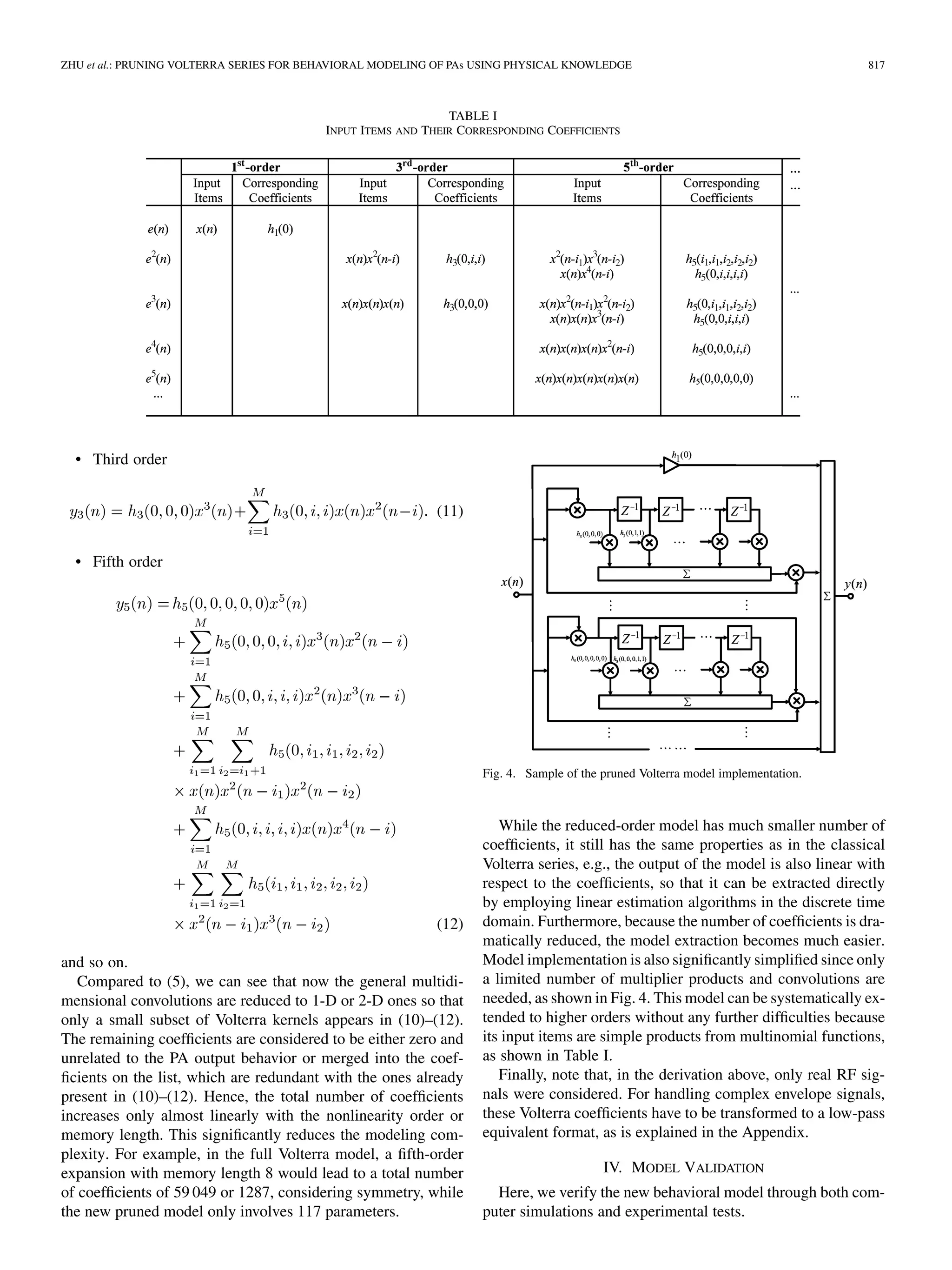
![818 IEEE TRANSACTIONS ON MICROWAVE THEORY AND TECHNIQUES, VOL. 55, NO. 5, MAY 2007
A. Computer Simulations
In this first test, we designed an equivalent-circuit PA model
and simulated it with the Agilent’s Advanced Design System
(ADS) [19] simulation software package. This is a GaAs
MESFET class-A PA operating at 2 GHz, excited by 3GPP
W-CDMA signals of 3.84-Mc/s chip rate. The reason for using
computer simulations was that this virtual test setup enabled
us to easily control the PA nonlinearity and memory effects,
and also allowed us to eliminate noise and measurement errors,
which may mask the actual model accuracy.
This PA was simulated by a co-simulation of Ptolemy and the
Circuit-Envelope Simulator in ADS 2004A [19]. Although the
proposed model can be employed to represent a wide range of
the PA’s nonlinear characteristics and memory effects, as the
general Volterra model, in this test, we only concentrated on
memory effects arising from the bias networks. Other memory
effects, such as self-heating and trapping effects, were not con-
sidered since the MESFET nonlinear model did not include
them.
To investigate the capability of our model in representing PA
memory effects, we simulated the amplifier circuit under two
different bias networks, which were: 1) ideal, in which the dc
feed is close to the ideal short circuit and 2) nonideal, in which
the dc feed shows a nonnegligible impedance to the envelope
frequency components. The resulting dynamic AM/AM plots
are shown in Fig. 5. From these plots, we can see that the PA did
not present any significant memory under ideal bias networks,
while memory became evident (AM–AM plots showing distinct
hysteresis loops) when the bias impedance increased, some-
thing to be expected from a real PA. As discussed in Section II,
these memory effects were mainly present in the nonlinear op-
erating region since they arise from remixing the original input
with low/high-frequency harmonics and intermodulation prod-
ucts fed back from the output.
Fifty sets of time-domain envelope waveforms were captured
from the input and output of the PA under different output power
levels, and with a sampling rate of 30.72 MHz. These data were
then used for model extraction and model validation. The model
was truncated to fifth-order nonlinearity with memory length
from three to eight, and was extracted via a least squares (LS) al-
gorithm in the discrete time domain. A sample of the output time
domain complex envelopes’ magnitude and phase are shown in
Fig. 6(a) and (b), respectively. These results clearly show that
the modeled data indeed fitted the desired outputs very well.
The normalized mean square errors (NMSEs) were calculated
for various validation data, and the average of them was ap-
proximately 43 dB, which indicates that the relative errors be-
tween the modeled and simulated time domain outputs were less
than 0.005%. For comparison, a fifth-order complex polyno-
mial (memoryless) model was also extracted for this PA, whose
output waveforms are shown in Fig. 6. Although the phase part
was fitted well, errors appeared in the magnitude. The NMSE for
this model only reached 29 dB. To show the model accuracy in
the frequency domain, the spectra of modeled errors are plotted
in Fig. 7. There we can see that the error signal spectrum of the
new model is almost close to the noise floor, while significant
errors are generated in the output predicted by the memoryless
Fig. 5. Sample AM/AM plots for the PA with: (a) ideal bias networks and
(b) nonideal bias networks.
model. For reference, the spectrum of the simulated output is
also plotted in Fig. 7.
B. Experimental Tests
To make this modeling technique closer to the “real” world,
we also tested a commercial LDMOS class-AB PA in our lab-
oratory. Its schematic diagram is depicted in Fig. 8. This PA,
operated at 2.14 GHz, and was excited by W-CDMA signals of
a 3.84-Mc/s chip rate and with 8.2-dB peak-to-average power
ratio (PAPR). The average output power of the PA is 10 W, and
its AM/AM characteristics were close to the ones seen in the
first simulated PA circuit.
The test bench setup used the ADS–electronic signal gen-
erator (ESG)–VSA connected solution [20]. The modulated
W-CDMA data files were first created at baseband, downloaded
to the arbitrary waveform generator, as complex in-phase (I)
and quadrature (Q) signals, and were then fed to the IQ modu-
lator present in the ESG. This generator was used to produce
the RF test signal to the PA. The output of the PA was then
down-converted and sampled by the vector signal analyzer
(VSA). To eliminate noise and measurement errors, 30 repeated](https://image.slidesharecdn.com/15486473-250612061438-3db84195/75/Ieee-Mttv055i05-200705-05th-Edition-Fantomasping-13-2048.jpg)

![820 IEEE TRANSACTIONS ON MICROWAVE THEORY AND TECHNIQUES, VOL. 55, NO. 5, MAY 2007
TABLE II
GAIN AND ACPR PERFORMANCE
since this number increases almost linearly with the order of the
nonlinearity or memory length.
V. CONCLUSION
An efficient and effective Volterra model pruning method for
RF PAs has been presented in this paper. The advantage of this
model reduction approach is that it allows efficient reduction of
the model complexity, while keeping all essential physical prop-
erties of a real PA since it was derived from a functional block
model, which has a clear linkage to the device’s physical be-
havior. Both computer simulation and experimental verification
tests indicated that this model can be employed to model a PA
with very high accuracy, but with a much smaller number of co-
efficients than the commonly used general Volterra models.
APPENDIX
In system level analysis and design, most simulators use base-
band complex envelope signals to evaluate the system perfor-
mance since modulation techniques are normally employed to
carry useful information. For handling these carrier-modulated
signals, the real bandpass Volterra coefficients and their corre-
sponding inputs have to be transformed into the complex en-
velope format. For example, the real kernel be-
comes the complex kernel where indicates a
complex conjugate transform need be made to its corresponding
input term , namely, its corresponding input is
, where represents the complex con-
jugate transform. The details of the transforms are as follows.
• First order
(a1)
• Third order
(a2)
(a3)
• Fifth order
(a4)
(a5)
(a6)
(a7)
(a8)
(a9)
The higher order kernels can be derived in the same way.
REFERENCES
[1] M. Schetzen, The Volterra and Wiener Theories of Nonlinear Systems,
reprint ed. Melbourne, FL: Krieger, 1989.
[2] J. C. Pedro and S. A. Maas, “A comparative overview of microwave
and wireless power-amplifier behavioral modeling approaches,” IEEE
Trans. Microw. Theory Tech., vol. 53, no. 4, pp. 1150–1163, Apr. 2005.
[3] C. P. Silva et al., “Optimal-filter approach for nonlinear power ampli-
fier modeling and equalization,” in IEEE MTT-S Int. Microw. Symp.
Dig., Boston, MA, Jun. 2000, pp. 437–440.
[4] H. Ku, M. Mckinley, and J. S. Kenney, “Quantifying memory effects
in RF power amplifiers,” IEEE Trans. Microw. Theory Tech., vol. 50,
no. 12, pp. 2843–2849, Dec. 2002.
[5] J. Kim and K. Konstantinou, “Digital predistortion of wideband signals
based on power amplifier model with memory,” Electron. Lett., vol. 37,
no. 23, pp. 1417–1418, Nov. 2001.
[6] A. Zhu and T. J. Brazil, “Behavioral modeling of RF power ampli-
fiers based on pruned Volterra series,” IEEE Microw. Wireless Compon.
Lett., vol. 14, pp. 563–565, Dec. 2004.
[7] C. Silva, A. Moulthrop, and M. Muha, “Introduction to polyspectral
modeling and compensation techniques for wideband communications
systems,” in 58th ARFTG Conf. Dig., San Diego, CA, Nov. 2001, pp.
1–15.
[8] D. Mirri et al., “A nonlinear dynamic model for performance analysis
of large-signal amplifiers in communication systems,” IEEE Trans. In-
strum. Meas., vol. 53, no. 2, pp. 341–350, Apr. 2004.
[9] E. Ngoya et al., “Accurate RF and microwave system level modeling of
wideband nonlinear circuits,” in IEEE MTT-S Int. Microw. Symp. Dig.,
Boston, MA, Jun. 2000, vol. 1, pp. 79–82.
[10] A. Zhu, J. Dooley, and T. J. Brazil, “Simplified Volterra series based be-
havioral modeling of RF power amplifiers using deviation reduction,”
in IEEE MTT-S Int. Microw. Symp. Dig., 2006, pp. 1113–1116.
[11] A. Zhu, J. C. Pedro, and T. J. Brazil, “Dynamic deviation reduction-
based Volterra behavioral modeling of RF power amplifiers,” IEEE
Trans. Microw. Theory Tech., vol. 54, no. 12, pp. 4323–4332, Dec.
2006.
[12] A. Zhu and T. J. Brazil, “RF power amplifiers behavioral modeling
using Volterra expansion with Laguerre functions,” in IEEE MTT-S Int.
Microw. Symp. Dig., 2005, pp. 963–966.
[13] M. Isaksson and D. Rönnow, “A Kautz–Volterra behavioral model for
RF power amplifiers,” in IEEE MTT-S Int. Microw. Symp. Dig., 2006,
pp. 485–488.
[14] J. C. Pedro, N. B. Carvalho, and P. M. Lavrador, “Modeling nonlinear
behavior of bandpass memoryless and dynamic systems,” in IEEE
MTT-S Int. Microw. Symp. Dig., Philadelphia, PA, Jun. 2003, vol. 3,
pp. 2133–2136.
[15] E. Ngoya and A. Soury, “Envelope domain methods for behavioral
modeling,” in Fundamentals of Nonlinear Behavioral Modeling for RF
and Microwave Design. Norwood, MA: Artech House, 2005, ch. 3,
pp. 37–86.
[16] J. C. Pedro and N. B. Carvalho, Intermodulation in Microwave and
Wireless Circuits. Norwood, MA: Artech House, 2003.
[17] J. Vuolevi, T. Rahkonen, and J. Manninen, “Measurement technique for
characterizing memory effects in RF power amplifiers,” IEEE Trans.
Microw. Theory Tech., vol. 49, no. 8, pp. 1383–1389, Aug. 2001.
[18] J. Vuolevi and T. Rahkonen, Distortion in RF Power Amplifiers. Nor-
wood, MA: Artech House, 2003.
[19] Advanced Design System (ADS) 2004A. Agilent Technol., Palo Alto,
CA [Online]. Available: http://eesof.tm.agilent.com/
[20] “Connected simulation and test solutions using the advanced design
system,” Agilent Technol., Palo Alto, CA, Applicat. Notes 1394, 2000.](https://image.slidesharecdn.com/15486473-250612061438-3db84195/75/Ieee-Mttv055i05-200705-05th-Edition-Fantomasping-15-2048.jpg)

![822 IEEE TRANSACTIONS ON MICROWAVE THEORY AND TECHNIQUES, VOL. 55, NO. 5, MAY 2007
Modeling Superconducting Transmission Line Bends
and Their Impact on Nonlinear Effects
Jordi Mateu, Member, IEEE, Carlos Collado, Member, IEEE, and Juan M. O’Callaghan, Senior Member, IEEE
Abstract—This paper reports on a numerical technique to ob-
tain the current distribution in the annular bent sections of planar
layouts. This is used to obtain the linear and nonlinear circuit dis-
tributed parameters modeling a superconducting strip bend and
its impact on intermodulation distortion. As an example, we ana-
lyze a superconductive open-loop resonator and assess the linear
and nonlinear contribution of its bends in its overall linear and
nonlinear performance. These simulations are very useful for opti-
mizing the resonators of a filter in order to minimize its nonlinear
distortion.
Index Terms—Circuit model, current distribution, nonlinear ef-
fects, superconductor, transmission line.
I. INTRODUCTION
LOW LOSSES of high temperature superconductive (HTS)
thin films allow the fabrication of very compact and high-
performance microwave filters [1], [2]. These planar devices
often include narrow strip topologies with numerous multicou-
pled transmission lines [3] and bends. This usually leads to high
current densities in the superconductor even at low input power
[4], which not only affects the linear response of the filter, but
may also give rise to undesirable nonlinear effects like intermod-
ulation distortion (IMD) [5], [6]. An accurate modeling of these
bends, particularly the current distribution in their cross section,
is thus necessary to be able to model the linear and nonlinear re-
sponse of superconducting devices, especially filters.
In straight transmission lines, there are well-known proce-
dures to find the current distribution in the cross section of the
line and calculate its inductance and resistance per unit length
from it [7]–[9]. If the line is made from superconductor
materials, this current distribution is known to change with the
current through the line due to the properties of the supercon-
ductor (i.e., the current dependence of its penetration depth)
[10]. This gives rise to a dependence of and on the current
Manuscript received September 14, 2006; revised January 11, 2007.
This work was supported in part under the Fulbright Program and by the
Spanish Government (CICYT) under Grant MAT-2005-05656-C03 and Grant
TEC-2006-13248-C04-02/TCM and under the Ramón y Cajal Program through
RyC-001125.
J. Mateu is with the Department of Signal Theory and Communications, Uni-
versitat Politècnica de Catalunya, Barcelona 08034, Spain, and also with the
Centre Tecnològic de Telecomunicacions de Catalunya, Universitat Politècnica
de Catalunya, 08860-Castelldefels, Barcelona, Spain (e-mail: jmateu@tsc.upc.
edu).
C. Collado and J. M. O’Callaghan are with the Department of Signal Theory
and Communications, Universitat Politècnica de Catalunya, Barcelona 08034,
Spain (e-mail: collado@tsc.upc.edu; joano@tsc.upc.edu).
Color versions of one or more of the figures in this paper are available online
at http://ieeexplore.ieee.org.
Digital Object Identifier 10.1109/TMTT.2007.895166
of the line, which provokes nonlinear effects. The calculation of
the dependence of the current distribution on total current and
its effects on and are well established for straight supercon-
ducting transmission lines [6], [10], but not for bent segments
of lines.
The goal of this paper is to fill in this void, i.e., adapt the
methods used in straight transmission lines to find the current
distribution in a cross section of an annular bent transmission
line, find its impact on and , and in the case of supercon-
ducting lines, find how and depend on current and how this
impacts IMD in a typical resonator that could be used in a su-
perconducting filter.
In Section II, we describe the Weeks–Sheen method [7],
[8] used to calculate and in normal and superconducting
straight transmission lines and our extension for the linear
modeling of annular bent sections. We will refer to the latter
as the radial Weeks–Sheen method. Although this method
is actually applied to annular bent sections, we will use the
single term bend to refer to them throughout this paper. We
also describe a cross check of this method where we analyze
a copper microstrip bend and compare our results with those
obtained with two alternative methods of the inductance per
unit length in a normal conductor. Section III shows how to
consider the nonlinear effects existing in superconducting
materials using the distribution of the current density in a cross
section of the bend obtained from the radial Weeks–Sheen
method. Finally, in Section IV, we use this approach to predict
the effects of bends in the linear and nonlinear response of a
half-wave square-shaped open-loop resonator.
II. WEEKS–SHEEN METHOD FOR CURVED
TRANSMISSION LINES
A. Theoretical Background
To evaluate the resistance and inductance per unit length of
the strip, i.e., and , one needs to know the volume current
density distribution over the cross section of the line. This can be
done using the Weeks et al. method [7], later modified by Sheen
et al. [8] for superconductive transmission lines. This section
shows the basics of the Weeks–Sheen method to illustrate how
it is modified to be able to undertake the analysis of bent regions.
The cross section of the strip is meshed in smaller transmis-
sion lines resulting in a system of coupled transmission line
equations. Fig. 1(a) shows a schematic diagram illustrating
the meshing of a straight elemental segment of length . The
meshing distribution is usually performed based on a priori
intuition of the current distribution profile; i.e., choosing the
smallest patches where the current distribution changes sharply
0018-9480/$25.00 © 2007 IEEE](https://image.slidesharecdn.com/15486473-250612061438-3db84195/75/Ieee-Mttv055i05-200705-05th-Edition-Fantomasping-17-2048.jpg)
![MATEU et al.: MODELING SUPERCONDUCTING TRANSMISSION LINE BENDS AND THEIR IMPACT ON NONLINEAR EFFECTS 823
Fig. 1. Meshing of the cross section of the strip. (a) For a straight segment of
the strip. (b) For a bent segment of the strip. r defines the curvature of the
bend, w and t define the width and thickness of the strip, respectively.
[9], this reduces the required number cells of the meshing and,
therefore, reduces the computation time.
The resulting multicoupled transmission lines should satisfy
the telegrapher’s equation [7]
(1)
where is the vector containing the variation of the voltage
of each patch relative to a reference patch—usually located in
ground plane—as a function of the length of the segment , and
is the vector containing the current in each line. is the matrix
of self and mutual impedances per unit length between patches
(2)
with and being resistances and inductances per unit length.
The matrices may be calculated following the procedure dis-
cussed in detail by [8] (or [7] for normal conductors). Here, we
just point out the expressions used to calculate the elements of
and . We write the elements in these matrices as and ,
respectively, where and indicate the corresponding row and
column. The resistive elements are given by
(3)
where for and for , and indi-
cate the area and the complex conductivity of the patch th. The
complex conductivity can be written as (where
, being the superconducting penetration
depth). The calculation of is somehow more complicated
and can be split in a kinetic inductance ( , only existing in
the superconducting case) and a partial inductance . The
partial inductance includes the internal and external inductance
corresponding, respectively, to the energy stored inside and out-
side of each conductor segment, due to the magnetic field, and
can be obtained from [8, eqs. (11) and (12)]. The kinetic induc-
tance can be obtained from the imaginary part of the supercon-
ducting impedance as [8]
(4)
As done in [8], we assume that the line voltages are quasi-
static, thus the voltages in the patches of the signal line are set to
a constant value and 0 for patches of the ground plane. From
a practical point-of-view, this implies that the term takes
a constant value for the patches in the signal strip and is 0 for
Fig. 2. Outline of one individual patch segment corresponding to a bent seg-
ment of the structure of Fig. 1(b).
the ground plane patches. Thus, (1) may be solved by inverting
the impedance matrix
(5)
with being the admittance matrix . This gives us
the current flowing through each line, which may be used to cal-
culate the current density distribution . By an algebraic addi-
tion of the elements from the admittance matrix corresponding
to the signal line, that are in parallel, one obtains the admittance
of the line and, thus, its inductance and resistance per
unit of length [8].
B. Radial Weeks–Sheen Method
The purpose here is to modify the conventional Weeks–Sheen
method to obtain the distributed parameters describing a bent
elemental segment. Fig. 1(b) shows a schematic of a meshed
bent elemental segment. Unlike the straight elemental segment
of Fig. 1(a), in a bent region [see Fig. 1(b)], the elemental length
may be different for each line resulting from the meshing. We
use, therefore, the angle to define the best elemental sement
of Fig. 1(b).
To analyze this structure, we first begin by considering a
single segment of the meshed region. Fig. 2 outlines the th
segment. The length of this segment is and can be related
with the angle defining the bent region and the radius of the
th patch segment as .
Considering the geometrical parameters defining each of the
segments of a bend, (1) can be rewritten as
(6)
where is the voltage drop in a segment of length and is
the current flowing through the th segment. The total number
of segments is defined by the meshing. By considering
, (6) can then be written as
(7)
which in matrix form is
(8)
where the matrix is diagonal and is a vector containing
the radius of each segment of the bend .
Note that since the cross section of a straight elemental segment](https://image.slidesharecdn.com/15486473-250612061438-3db84195/75/Ieee-Mttv055i05-200705-05th-Edition-Fantomasping-18-2048.jpg)
![824 IEEE TRANSACTIONS ON MICROWAVE THEORY AND TECHNIQUES, VOL. 55, NO. 5, MAY 2007
[see Fig. 1(a)] is equal to the cross section of a bent elemental
segment [see Fig. 1(b)], the values of the matrix should also
be equal. Thus, we can define the equivalent matrix, which char-
acterizes the cross section of the bent segment as
(9)
The resulting equation of a multicoupled bent transmission
lines is
(10)
By following the same procedure used to solve (1), we may
obtain the current flowing through each patch of the bent seg-
ment from (10) as follows:
(11)
where is the equivalent admittance matrix of a bent re-
gion and the term is constant for each segment belonging
to the signal strip. From , we obtain the inductance
and resistance of the bent transmission line per unit angle.
The inductance and resistance per unit length and can be
straightforwardly obtained by dividing and by the radius
defining the curvature of the bend . is defined
from the middle of the bend, thus its minimum value would be
.
C. Cross-Check for a Normal Conductor Bend
Here, we apply the radial Weeks–Sheen method for a normal
conductor to be able to compare the results with existing tech-
niques. This can be done by considering a real conductivity [7],
which allows us to neglect (4) in the impedance matrix calcu-
lation. The microstrip bend has a cross section with 0.5 mm of
width and 0.43 mm of substrate thickness.
Two different approaches, contained in a commercial soft-
ware package [12], have been used to obtain the inductance
per unit length of a copper bend as a function of its radius.
The first approach consists of a microstrip circuit model for
curved bends based on perturbation techniques [13]. Its results
are shown in the squares in Fig. 3. In this case, we see how
the effects of the bend start for , smoothly re-
ducing the distributed inductance as the radius decreases. The
second approach performs electromagnetic simulation of the
planar structure by using techniques based on the method of mo-
ments [12]. The results are shown in triangles in Fig. 3. Finally,
the dashed line in Fig. 3 shows the results using the method we
propose. The latter two methods show very good agreement for
the whole range of and predict a weak dependence of
on for values of and a sharp decrease
for smaller values of .
III. NONLINEAR SUPERCONDUCTING BENDS
A. Calculation of the Nonlinear Parameters
In a superconducting case, the nonlinear dependence
of the superfluid density on the current density gives
rise to a nonlinear complex conductivity [6],
Fig. 3. Variation of the distributed inductance of a cooper microstrip bend (L)
as a function of r . Squares represent the results obtained using the circuit
model based on [13], triangles correspond to the full-wave simulation results
and the dashed line corresponds to the simulation with our technique.
. In this equation, the conductivity
of normal fluid and the penetration depth of the super-
condutor depend on temperature and current density
as
(12)
where the function describes the form of the nonlin-
earity and relates the relative magnitudes of the real and
imaginary components of the nonlinear conductivity [6].
To evaluate these deviations, we use an iterative procedure
[10], which, from the current distribution of the current iteration
updates and of the next iteration using (12). From
these new values, we recalculate the current distribution and re-
peat this procedure until convergence is achieved. By running
this procedure for several values of voltage in the signal strip
, we determine the nonlinear current dependence of the induc-
tance and resistance per unit of length. Note that
the nonlinear current dependence of the distributed inductance
is only due to the variation of the kinetic part of the inductance.
We assume a quadratic nonlinear dependence of the super-
fluid density on the current density, i.e.,
( being a characteristic current density that sets the
strength of nonlinearities), which is a very good approximation
for weak nonlinear effects [10]. In this case, the
resulting distributed parameters [ and ] can
be obtained from closed-form equations and also follow a
quadratic dependence on the current flowing through the line
(13)
where the nonlinear terms and can be found
from the following expressions [14]:
(14)](https://image.slidesharecdn.com/15486473-250612061438-3db84195/75/Ieee-Mttv055i05-200705-05th-Edition-Fantomasping-19-2048.jpg)
![MATEU et al.: MODELING SUPERCONDUCTING TRANSMISSION LINE BENDS AND THEIR IMPACT ON NONLINEAR EFFECTS 825
where is a geometrical factor , which depends on the current
density distribution over the cross section
(15)
The nonlinear dependence of the distributed resistance and in-
ductance using (13)–(15) has been verified using the above out-
lined iterative procedure [10]. This procedure may show diver-
gence for high current densities or strong nonlinear effects. Al-
though the range of validity may be improved using a more ro-
bust iterative procedure, we estimate the validity of this method
for .
In Section III, we will evaluate these quantities for a straight
and bent segment of a strip, such as the ones shown in Fig. 1.
B. Modeling of a Microstrip Bend
Here, we use the above-described procedure to obtain the
linear and nonlinear distributed parameters ( and ) in a
microstrip superconducting bent transmission line as a function
of its radius.
The cross section used for this example is a microstrip
structure where the width of the signal line is 0.5 mm, the
thickness of the superconducting strip and ground plane is
270 nm, and the thickness of the dielectric substrate is 0.43 mm.
The material is YBCO on MgO. The surface resistance of the
material at 77 K and 10 GHz is 0.7 m and the penetration
depth at 77 K is 230 nm. The simulations are performed at
2 GHz since it is a frequency of interest in wireless communi-
cation applications. Note that the topology of the structure and
properties of the material considered for this simulation are
commonly used in superconducting filter designs [15].
Fig. 4 depicts the current density distribution in the cross sec-
tion for a straight transmission line [see Fig. 4(a)] and for a bent
transmission line with [see Fig. 4(b)]. The cur-
rent density distribution in a straight line segment has a sym-
metric profile, whereas in the bent segment, as we expect, the
current density distribution is higher at the inner part. As we
will show below, this has consequences on both the linear and
nonlinear parameters defining the circuit model of the line.
To evaluate the effects of the bend in the linear parameters
defining the bent transmission line, Fig. 5 shows the linear in-
ductance and resistance per unit length as a func-
tion of the ratio between the radius of the bend and the width
of the line . Note also that and in Fig. 5
are normalized by the inductance and resistance of
a straight segment. These results show a reduction of the in-
ductance and an increment of the resistance when the radius
decreases. Note that, to guarantee a less than 10% deviation
with respect to the straight-line values of , should
be kept above 1. This condition is slightly more stringent for
.
We have also assessed the impact of the bends in the nonlinear
performance of a superconducting transmission line. To do this,
we assume the quadratic nonlinear behavior of Section II-A and
determine how the geometric factor changes with .
Fig. 4. Volume current density distribution over the signal strip of microstrip
topology. (a) For a straight elemental segment. (b) For a bent elemental segment
with r =w = 0:8.
Fig. 5. (left) Variation of the distributed inductance of a bend (L ) as a func-
tion of r . (right) Variation of the distributed resistance of a bend (R ) as
a function of r . Both are normalized by the distributed parameters in a
straight segment, L and R , respectively.
Fig. 6 depicts the dependence of on the radius of the bent seg-
ment. We see that the nonlinearities may increase by a factor of
20 when the radius gets close to , which is likely to affect](https://image.slidesharecdn.com/15486473-250612061438-3db84195/75/Ieee-Mttv055i05-200705-05th-Edition-Fantomasping-20-2048.jpg)
![826 IEEE TRANSACTIONS ON MICROWAVE THEORY AND TECHNIQUES, VOL. 55, NO. 5, MAY 2007
Fig. 6. Nonlinear geometrical factor 0 (9) as a function of the radius of the
bent segment normalized by 0 in a straight segment.
Fig. 7. Open-loop resonator IMD products (in decibels) as a function of the
r =w normalized by the IMD in a straight resonator. Solid, dashed, and
dotted lines correspond to x = =40, =20, and =10, respectively. Variation
of the normalized quality factor (Q =Q ) as a function of r =w. Note
that, in this layout, the effect of the gap length is neglected.
the overall nonlinear performance of the device containing the
bend.
The effects shown above are very important from an engi-
neering point-of-view since it is necessary to predict them for a
proper design of resonator and filter topologies. Note also that
this is relevant for materials characterization since many planar
devices used to obtain linear and nonlinear parameters to char-
acterize the superconducting materials use planar patterns con-
taining bends [16], [17].
Here, it has been shown how the distributed parameters in a
bent segment deviate from the ones expected in a straight seg-
ment. Section IV goes one step further, showing the application
of these results to evaluate the effects of bent regions in practical
microwave devices.
IV. OPEN-LOOP RESONATORS WITH BENDS
Here, we analyze how the linear and nonlinear performance
of an open-loop resonator is affected by the radius of the bend
and by the position where the bends are located. The
inset of Fig. 7 outlines the topology of the open-loop under
study. It contains four bends, two of them are placed at a dis-
tance from the open ends of the resonator and the other two at
a distance from the center. The cross section and parameters
of the resonator are the ones used in Section IV-A. The length of
the resonator has been adjusted to operate on its first resonant
mode (i.e., half-wave resonator) at 2 GHz. That is the current
distribution, which follows a sinusoidal distribution along the
resonator.
To analyze this structure, we have split the resonator in
straight regions and bent regions (see the inset of Fig. 7). The
equivalent-circuit model of the whole resonator consists of
concatenating many elemental RLCG cells, corresponding to a
straight or a bent region.
The equivalent circuit can now be solved either using a circuit
analysis tool (note that it should be able to apply nonlinear anal-
ysis, such as harmonic-balance techniques [18]) or by devel-
oping the closed-form expression, which gives the IMD prod-
ucts generated along the resonator of length . We have obtained
this expression by following the procedure detailed in [6]. Un-
like [6], in this case, we should consider the dependence of the
circuit parameters ( and ) on their location along the
resonator.
To do that, we assume a spatial sinusoidal distribution of the
fundamental and IMD frequencies. For quadratic nonlinearities
[see (13)], the nonlinear voltage at IMD frequency in an ele-
mental segment of the resonator is
(16)
where and are the current of the fundamen-
tals. Now the power generated at IMD frequency
will be dissipated in the
resonator (dielectric losses are assumed negligible [9]) and
coupling loads , where is
the coupling coefficient [19] and, thus, the term accounts
for the dissipation on the input and output, assuming equal
coupling. Note that these integrals should consider the value of
the linear and nonlinear distributed parameter at each position
of the resonator. Once we know , the power at the IMD
frequency coupled to the load is
(17)
This expression has been verified by simulating the equiva-
lent circuit of the whole resonator of the inset of Fig. 7, which
consists of cascading many RLCG elemental cells, using a cir-
cuit analysis simulator [12].
The results of this analysis are shown in Fig. 7. The right-hand
axis indicates the quality factor of the half-wave open-loop res-
onator normalized by the quality factor in a half-wave straight
resonator. The quality factor decreases when decreases.
We see that, for , the quality factor drops more
than 10%, and for , it degrades more than 30%.
The quality factor is barely affected by the position of the bents.
The left-hand axis in Fig. 7 indicates the IMD of the open-loop
resonator normalized by the IMD that occurs in a straight res-
onator. These results show how the nonlinearities rapidly in-
crease when decreases. When , the IMD](https://image.slidesharecdn.com/15486473-250612061438-3db84195/75/Ieee-Mttv055i05-200705-05th-Edition-Fantomasping-21-2048.jpg)
![MATEU et al.: MODELING SUPERCONDUCTING TRANSMISSION LINE BENDS AND THEIR IMPACT ON NONLINEAR EFFECTS 827
increases more than 4 dB, and for , it increases
more than 10 dB. As occurs with the quality factor, the IMD is
not strongly affected by the position of the bends. This may be
explained by assuming a sinusoidal distribution along the strip.
When increases (or decreases), the two bends closer to the
ends have a stronger (or weaker) contribution, whereas the other
two bends have a weaker (or stronger) contribution. Note that
these effects depend on the resonator topology.
The resonant frequency of the resonator would also be af-
fected by the bent segments contained in the structure. This can
be concluded from the deviation of the distributed inductance
as a function of the radius in Fig. 3. However, the bends would
also introduce an additional distributed capacitance [19], which
will also affect the resonant frequency of the structures, thus
we cannot obtain the frequency shift in the resonator only from
the deviation of the inductance due to the bent segments. Note
that this would not occur for the quality factor since the losses
coming from the dielectric (which are also affected by the bent
section) are negligible [6]. Although the frequency shift is a
very important designing parameter, in practice, this can usu-
ally be tuned by making the resonator slightly longer or shorter,
whereas the quality factor and IMD are parameters that strongly
depend on the shape of the resonator (and material properties)
and cannot be tuned for a given geometry.
V. CONCLUSION
The radial Weeks–Sheen method proposed in this paper has
been shown to be consistent with other methods of analyzing
normal conducting bends of planar microwave circuits. Unlike
the methods used in the comparison, the radial Weeks–Sheen
method is also applicable to superconductors and can be used
to predict the linear and nonlinear effects of a bend. We have
analyzed a typical microstrip geometry and we found that, to
keep the inductance per unit length in the bend within 10% of
its value in a straight line, should be kept higher than 1
in both a superconducting and a normal-metal strip (Figs. 3 and
5). This condition is slightly more stringent for the resistance
per unit length of a superconducting strip .
When analyzing the nonlinear effects of bends in an
open-loop resonator at 2 GHz (Fig. 7), we found that when
, decreases approximately 10% with respect to
that of a straight-line resonator, and IMD increases by 2–3 dB
depending on the position of the bends. In any case, both IMD
and degrade significantly for lower values of ,
which would make them inadequate for high-performance
superconducting filters.
While this paper and its conclusions have an obvious rele-
vance for microwave engineering purposes, they may also be
of interest for testing superconductors since many test devices
consist of planar circuits containing strip bends.
ACKNOWLEDGMENT
The authors would like to thank Dr. R. Taylor and R. Clarke,
both with Microwave and Materials Designs Pty. Ltd., Brisbane,
Australia, for fruitful discussions and comments.
REFERENCES
[1] J.-S. Hong and M. J. Lancaster, “Compact microwave elliptic function
filter using novel microstrip meander open-loop resonators,” Electron.
Lett., vol. 32, pp. 563–564, 1996.
[2] H. Su and M. J. Lancaster, “Highly miniature HTS microwave filters,”
IEEE Trans. Appl. Supercond., vol. 11, no. 1, pp. 349–352, Mar. 2001.
[3] J. Mateu, C. Collado, and J. M. O’Callaghan, “Nonlinear model of cou-
pled superconducting lines,” IEEE Trans. Appl. Supercond., vol. 15, no.
2, pp. 976–979, Jun. 2005.
[4] D. E. Oates, S.-H. Park, D. Agassi, G. Koren, and K. Irgmaier, “Tem-
perature dependence of intermodulation distortion in YBCO: Under-
standing nonlinearity,” IEEE Trans. Appl. Supercond., vol. 15, no. 2,
pp. 3589–3595, Jun. 2005.
[5] M. I. Salkola, “Nonlinear characteristics of a superconducting re-
ceiver,” Appl. Phys. Lett., vol. 88, pp. 012501/1–012501/3, 2006.
[6] C. Collado, J. Mateu, and J. M. O’Callaghan, “Analysis and simula-
tion of the effects of distributed nonlinearities in microwave supercon-
ducting devices,” IEEE Trans. Appl. Supercond., vol. 15, no. 1, pp.
26–39, Mar. 2005.
[7] W. T. Weeks, L. L. Wu, M. F. McAllister, and A. Singh, “Resistive and
inductive skin effect in rectangular conductors,” IBM J. Res. Dev., vol.
23, pp. 652–660, 1979.
[8] D. M. Sheen, S. M. Ali, D. E. Oates, R. S. Whiters, and J. A. Kong,
“Current distribution, resistance, and inductance for superconducting
strip transmission lines,” IEEE Trans. Appl. Supercond., vol. 1, no. 2,
pp. 108–115, Jun. 1991.
[9] A. Porch, M. J. Lancaster, and R. G. Humphreys, “The coplanar res-
onator technique for determining the surface impedance of YBaCO thin
film,” IEEE Trans. Microw. Theory Tech., vol. 43, no. 2, pp. 306–314,
Feb. 1995.
[10] T. Dahm and D. Scalapino, “Theory of intermodulation in super-
conducting microstrip resonator,” J. Appl. Phys., vol. 81, no. 4, pp.
2002–2006, 1997.
[11] J. C. Booth, J. Bell, D. Rudman, L. Valle, and R. Ono, “Geometry de-
pendence of nonlinear at microwave frequencies,” J. Appl. Phys., vol.
86, no. 2, pp. 1020–1025, 1999.
[12] Advanced Design System. Agilent Technol., Palo Alto, CA, 2005.
[13] A. Weisshaar and V. K. Tripathi, “Perturbation analysis and modeling
of curved microstrip bends,” IEEE Trans. Microw. Theory Tech., vol.
38, no. 10, pp. 1449–1454, Oct. 1990.
[14] J. C. Booth, K. Leong, S. A. Schima, C. Collado, J. Mateu, and J. M.
O’Callaghan, “Unified description of nonlinear effects in high temper-
ature superconductors,” J. Supercond. 2006.
[15] J.-S. Hong, M. J. Lancaster, D. Jedamzik, and R. B. Greed, “On the
development of superconducting microstrip filter for mobile commu-
nication applications,” IEEE Trans. Microw. Theory Tech., vol. 47, no.
9, pp. 1656–1663, Sep. 1999.
[16] Y. Wang, H. T. Su, F. Huang, and M. J. Lancaster, “Wide-band super-
conducting coplanar delay line,” IEEE Trans. Microw. Theory Tech.,
vol. 53, no. 7, pp. 2348–2354, Jul. 2005.
[17] Y. Wang, H. Su, F. Huang, and M. J. Lancaster, “Measurements of
YBCO surface resistance using coplanar line resonator techniques from
20 MHz to 20 GHz,” IEEE Trans. Appl. Supercond., submitted for pub-
lication.
[18] S. A. Maas, Nonlinear Microwave Circuits. Boston, MA: Artech
House, 1998.
[19] J.-S. Hong and M. J. Lancaster, Microstrip Filters for RF/Microwave
Applications, ser. Microw. Opt. Eng. New York: Wiley, 2001.
Jordi Mateu (M’03) was born in Llardecans,
Spain, in 1975. He received the Telecommunication
Engineering and Ph.D. degrees from the Universitat
Politècnica de Catalunya (UPC), Barcelona, Spain,
in 1999 and 2003, respectively.
Since October 2006, he has been Research Fellow
with the Department of Signal Theory and Commu-
nications, UPC. From May to August 2001, he was
Visiting Researcher with Superconductor Technolo-
gies Inc., Santa Barbara, CA. From October 2002 to
August 2005, he was Research Associate with the
Telecommunication Technological Center of Catalonia, Catalonia, Spain. Since
September 2004, he has held several Guest Researcher appointments with the
National Institute of Standards an Technology (NIST), Boulder, CO, where
he was a Fulbright Research Fellow from September 2005 to October 2006.
In July 2006, he was a Visiting Researcher with the Massachusetts Institute
of Technology (MIT) Lincoln Laboratory. From September 2003 to August](https://image.slidesharecdn.com/15486473-250612061438-3db84195/75/Ieee-Mttv055i05-200705-05th-Edition-Fantomasping-22-2048.jpg)

![IEEE TRANSACTIONS ON MICROWAVE THEORY AND TECHNIQUES, VOL. 55, NO. 5, MAY 2007 829
Analytic Large-Signal Modeling of
Silicon RF Power MOSFETs
Paolo Fioravanti, Member, IEEE, Oana Spulber, and Maria Merlyne De Souza, Member, IEEE
Abstract—This paper provides novel analytic expressions and
methodology for predicting the large-signal gain of RF power
MOSFETs. The expressions are derived from a model that in-
cludes input and output matching impedances, source inductance,
and gate resistance. Using the load line concept superimposed on a
nonlinear current generator, this paper demonstrates reasonably
accurate predictions of gain and gain compression point.
Index Terms—Circuit analysis, impedance matching, microwave
power amplifiers, semiconductor device model.
I. INTRODUCTION
HARMONIC-BALANCE (HB) simulations are the only vi-
able approach to provide accurate RF performance esti-
mation of devices in various applications. In the absence of HB,
analytic expressions can provide a quicker alternative. Unfortu-
nately, two-port and circuit derived [1] power gain expressions
for conventional MOSFETs are not appropriate for Si RF power
MOSFETs due to the substantial structural differences between
these two applications.
The most reliable analytical approaches available to date for
Si RF power MOSFETs have been proposed in [2] and [3].
These approaches considerably simplify the initial phases of cir-
cuit design through analytic expressions and methods for the
prediction of optimum matching impedances, power gain, and
gain compression. These expressions permit faster development
of circuital applications and prediction of device performance.
This information is particularly valuable due to the large effect
that the matching impedance causes on power gain and gain
compression of Si RF power MOSFETs.
On the other hand, the expressions in [2] neglect the effect
of the gate resistance of the device yielding inaccurate power
gain, whereas the gain compression in [3] does not consider the
effect of the matching impedances, limiting the usefulness of
the prediction.
This paper describes an extension of [2] to deduce matching
impedances and, for the first time, to include them in the deter-
mination of the gain compression.
Manuscript received October 27, 2006; revised February 6, 2007.
P. Fioravanti was with the Emerging Technologies Research Centre, De
Montfort University, Leicester LE1 9BH, U.K. He is now with Research and
Development, Theta Microelectronics, 15125 Athens, Greece.
O. Spulber was with the Emerging Technologies Research Centre, De Mont-
fort University, Leicester, LE1 9BH, U.K. She is now with International Recti-
fier, Newport NP10 8YJ, U.K.
M. M. De Souza is with the Emerging Technologies Research Centre, De
Montfort University, Leicester LE1 9BH, U.K. (e-mail: mms@dmu.ac.uk).
Color versions of one or more of the figures in this paper are available online
at http://ieeexplore.ieee.org.
Digital Object Identifier 10.1109/TMTT.2007.895403
Fig. 1. Transistor model including matching impedances, gate resistance,
source inductance, and a nonlinear voltage-controlled current generator. In [2],
R and g were not considered and I (V ) was assumed linear.
This paper is organized as follows. The background work of
[2]–[4] is described in Section II. In Section III, an improved
power gain expression is proposed to include the effect of the
gate resistance. The expression is then extended to the general
case of a nonlinear current generator. In Section IV, two proce-
dures for the determination of gain compression from the non-
linear current generator are presented. The accuracy of the pro-
posed expressions and procedures is verified in Section V via
comparison with HB simulations and measurements.
II. BACKGROUND
The effect of the load impedance on load–pull contours was
first analytically described by Cripps, who in 1983 demonstrated
simplified equations that lead to a good agreement with exper-
iment [4]. Following Cripps, a power gain expression was de-
rived in [2] based on the transistor model of Fig. 1 under the
assumption of a linear current generator, zero gate resistance,
and zero drain conductance.
The power gain and optimum source and load impedance
were given as
(1)
(2)
(3)
where is the angular frequency, is the source inductance,
is the gate-to-source capacitance, is the gate-to-drain
capacitance, is the drain-to-source capacitance, is the
transconductance, is the load line optimum resistance,
is the optimum load impedance, and is the optimum source
0018-9480/$25.00 © 2007 IEEE](https://image.slidesharecdn.com/15486473-250612061438-3db84195/75/Ieee-Mttv055i05-200705-05th-Edition-Fantomasping-24-2048.jpg)
![830 IEEE TRANSACTIONS ON MICROWAVE THEORY AND TECHNIQUES, VOL. 55, NO. 5, MAY 2007
impedance. The value of the model parameters are extracted at
the application frequency and bias. The transconductance value
considered in (1)–(3) varies with bias, reducing from the max-
imum in class A to in class B.
Another known expression that permits the calculation of the
power gain is
(4)
where is the amplifier load resistance, and
are the transconductance values associated with the intrinsic
MOSFET and the junction field-effect transistor (JFET) resis-
tance of Si RF power MOSFETs [3].
Equations (1)–(3) may be considered as an improvement with
respect to (4) because the latter does not include matching im-
pedances or the source inductance.
III. THEORETICAL ANALYSIS
Here, a new power gain expression is proposed to include the
effect of the gate resistance on the model in Fig. 1. The gain
expressions are first derived for a linear current generator and
subsequently adapted for the nonlinear case.
A. Effect of Gate Resistance on Power Gain
The expression in (1) overestimates the power gain, as can be
concluded from the results in [2]. Hence, to overcome this lim-
itation, in this study the model was modified to include the im-
pact of . Proceeding as in [2], the optimum load impedance
is determined by forcing the current generator to see a real
output impedance of value . As pointed out by Cripps [4],
[5], is the load line optimum resistance associated with
the maximum voltage and current swings. The optimum source
impedance is determined as the conjugate match of the tran-
sistor’s input impedance.
Circuit analysis of Fig. 1 reveals that
(5)
(6)
(7)
(8)
Using (5)–(8), the optimum load and source resistance are
now given as
(9)
(10)
The power and gain expressions are derived by defining
the input power as the power delivered to the transistor under
conjugate match conditions and the output power as the power
dissipated by the load-line resistance. These definitions yield
(11)–(13), shown at the bottom of this page.
It can be easily verified that (9), (10), and (13) coincide with
the expressions in [2] for and S.
B. Power Gain Expressions in the Nonlinear Case
Equation (13) can be used only for the determination of power
gain at small input signal levels, i.e., where the output is lin-
early proportional to the input. This occurs in the ideal transistor
case: the derivation implicitly assumes a constant value of the
transconductance and a linear drain current to input voltage re-
lationship. In this case only, the fundamental component of the
device current remains proportional to the input signal
through the transconductance value
(14)
However, real devices have transconductance values that are
neither constant, nor linearly dependent on the input voltage. In
the nonlinear current generator case, (14) cannot be considered
valid. The fundamental component of the current ( ) has to
be determined from the actual current waveform
(15)
where is the device output characteristic, is the gate
bias voltage, and is the input RF gate signal.
The determination of is demonstrated graphically
in Fig. 2. The device output characteristic needs to be ex-
tracted from the – curves. Conventionally this is carried
out considering a constant . However, in a real amplifier, the
device operates along the load line depending upon the class of
(11)
(12)
(13)](https://image.slidesharecdn.com/15486473-250612061438-3db84195/75/Ieee-Mttv055i05-200705-05th-Edition-Fantomasping-25-2048.jpg)

![832 IEEE TRANSACTIONS ON MICROWAVE THEORY AND TECHNIQUES, VOL. 55, NO. 5, MAY 2007
the maximum linear power. The input signal amplitude
at the 1-dB compression point is determined from the
third-order power series expansion of the current signal, as
described in [5]. In the single tone case, it can be stated as
(27)
with
(28)
The extraction of the optimum impedance will be clarified
with a practical example in Section V.
IV. METHODOLOGY FOR RF PERFORMANCE EVALUATION
The gain compression cannot be estimated from (13) since the
approach does not take device nonlinearity into account. Here,
an approach to predict gain compression based on the identifica-
tion of the fundamental current component from the output
drain current waveform is proposed. The determina-
tion of has been described in Section III-B.
Here, two approaches based on the Fourier analysis of the
current signal waveform are presented: the Fourier fundamental
approach (FFA), which is only suitable for single tone input
signals, and the Fourier spectrum approach (FSA), which is also
suitable for multitone input signals.
A. FFA
In the case of a periodic input waveform, it is possible to
express the generator current waveform by its Fourier
series expansion
(29)
with
(30)
(31)
(32)
(33)
(34)
where represents the amplitude of the signal of the th mul-
tiple of the fundamental frequency, is the period, and is the
angular frequency of the periodic input signal. For a single tone
input of angular frequency , the determination of the current
component at the fundamental frequency ( ) is carried
out using (29)–(34).
B. FSA
For a single-tone signal, it is relatively easy to calculate
from (15) using the approach of Fourier series as given by
(29)–(34). However, in the case of two closely spaced signals,
the above approach is limited by the accuracy of numerical
calculation and long computational times.
Hence, a Fourier spectrum analysis is required. The decom-
position of the current signal using the Fourier transform per-
mits the identification of the signal spectrum and the identifica-
tion of the frequency components of the current signal as
(35)
The generator current component at the fundamental fre-
quency ( ) is, therefore, determined. The Fourier transform
is carried out by applying the computationally efficient fast
Fourier transform (FFT) algorithm.
C. Calculation of the Power Gain Characteristic
The FFA and FSA permit the determination of the nonlinear
power gain characteristic by repetitive application. Due to the
dependence of in dependence on the input signal am-
plitude, the value of needs to be determined point by point
via the application of the FFA or FSA. Once has been cal-
culated for a sweep of input signal amplitudes, the application
of (19)–(26) yields the complete resolution of the equivalent cir-
cuit of Fig. 1 at the fundamental frequency .
V. RESULTS
In order to provide a benchmark for the assessment of the
accuracy of the proposed expressions, HB simulations have
been used. The simulations are carried out on the 28-V Polyfet
SP2041 in Agilent’s Advanced Design System (ADS) [6] using
the publicly available Polyfet model. The model predictions
shown in Figs. 4 and 5 permit adequate reconstruction of
measured characteristics and -parameters. In this study,
model components related to the package have been removed
to achieve direct correspondence between the calculated and
simulated impedance values. Alternatively, impedance trans-
formation can be carried out to include the effect of the package
[2]. Finally, a comparison is made between measured data and
prediction.
A. Extraction of the Device Parameters Values
The data used for the prediction of power gain based on the
proposed equations and approach is represented from the set of
– characteristics and the value of the model elements.
The – data extracted from ADS dc simulations is used
for the determination of the fundamental current component
. The values of the model elements are extracted at the ap-
plication voltage V from the results of a small signal
1Polyfet RF Devices, Camarillo, CA. [Online]. Available: http://www.
polyfet.com](https://image.slidesharecdn.com/15486473-250612061438-3db84195/75/Ieee-Mttv055i05-200705-05th-Edition-Fantomasping-27-2048.jpg)
![FIORAVANTI et al.: ANALYTIC LARGE-SIGNAL MODELING OF SILICON RF POWER MOSFETs 833
Fig. 4. ADS simulated versus measured I –V characteristics for the
Polyfet SP204.
Fig. 5. ADS simulated versus measured s-parameters for the Polyfet SP204.
TABLE I
PARAMETERS FOR THE POLYFET SP204
simulation. Table I indicates the values used in the calculations
throughout Section V.
At high frequency, considering capacitances as shorts, circuit
analysis shows that
(36)
(37)
and are extracted as the asymptotic values of
and , respectively. Their values are then deembedded
from the impedance matrix, as shown in [7].
After deembedding, the model parameter values can be ex-
tracted as
(38)
(39)
(40)
(41)
Fig. 6. Deembedding of source inductance and gate resistance from the small-
signal parameters circuit. (a) and (b) Measured s-parameter matrix S is con-
verted in the impedance matrix Z . Z refers to the equivalent circuit, which
includes R and L . R and L values are determined from the impedance
matrix Z using (36) and (37). Their values are deembedded from the impedance
matrix in (c), after [7]. The impedance matrix Z corresponds to the equiva-
lent circuit in which R and L have been removed. The admittance matrix Y
(without the R and L contribution) is obtained from the Z-parameter matrix
in (d). The admittance matrix Y is then used for model parameter extraction by
using (38)–(41).
The value in class A is calculated for a fixed supply
voltage V and V as
(42)
B. Optimum Source and Load Impedance
The optimum source ( ) and load ( ) impedance
values for class A bias are extracted from load– and source–pull
simulations using ADS as the values leading to the maximum
1-dB gain compression point. The optimum load impedance is
determined first. As in real load–pull measurements, is
identified as the load impedance yielding the highest possible
level of power delivered to the load for a constant input power
level. An impedance tuner is used as the amplifier load. As the
tuner impedance is varied, the corresponding power delivered to
the load changes. Keeping the input power constant ensures that
the variation of delivered power is associated only with the vari-
ation of the impedance. Measuring the delivered power for many
tuner impedance values permits the identification of the loci of
constant delivered power as a function of the load impedance.
The load–pull contours as shown in [7] and described in Fig. 6.
The optimum source impedance is determined analogously.
In this case, the impedance tuner is placed on the input side
and the optimum load impedance is placed at the output side
of the amplifier. Keeping the input power constant ensures that
the variation of power delivered to the load is associated only
with the variation of the tuner impedance. The loci of constant
delivered power as a function of the load and source impedance
are shown in Figs. 7 and 8. The optimum source impedance is
determined as the value associated with the maximum delivered
power level.
The following five different ways of calculating the optimum
impedance values are now assessed. The first three assume a
linear current generator in the equivalent model:
(i) without the inclusion of gate resistance;
(ii) including ( ) as described in Section III;
(iii) including and , as described in Section III.](https://image.slidesharecdn.com/15486473-250612061438-3db84195/75/Ieee-Mttv055i05-200705-05th-Edition-Fantomasping-28-2048.jpg)
![834 IEEE TRANSACTIONS ON MICROWAVE THEORY AND TECHNIQUES, VOL. 55, NO. 5, MAY 2007
Fig. 7. Load–pull delivered power contours in the class A single-tone
simulation.
Fig. 8. Source–pull delivered power contours in the class A single-tone
simulation.
The following two methods consider the nonlinear current
generator:
(iv) by using the FFA;
(v) by using the FSA.
In (iv) and (v), the calculations are carried out considering the
output characteristic extracted along the load line rather than the
fixed approach used to date.
An example of determination of the optimum load and source
impedance values is demonstrated for the nonlinear current gen-
erator cases (iv) and (v) with the device biased in class A at
V. The FSA is considered for this task. The calculated
impedance values are shown in Fig. 9. The source impedance
displays a strong dependence on the input signal level, while
the optimum load impedance is appreciatively constant. It can
be shown that this behavior follows from the existence of the
feedback elements and in the circuit. The optimum
values for the source and load impedance are extracted in cor-
respondence to the 1-dB compression point. The
value at which gain compression occurs is calculated by using
(27), yielding a value of 2.43 V.
The calculated optimum impedance values are compared
with those from ADS simulations. The power delivered to the
load, shown in Figs. 7 and 8, obtained by HB simulation in
Fig. 9. Calculated optimum source and load impedances in the single-tone
input signal case. The data refer to the application of the FSA. V is de-
termined with (23) after the determination of the power series coefficient c =
1:2866 [V ] and c = 00:0379 [V ] from the fit of the load line output
transfer characteristic.
TABLE II
POWER GAIN AT SMALL INPUT LEVELS, OPTIMUM LOAD
AND SOURCE IMPEDANCE VALUES
ADS, is used to assess the accuracy of the calculated impedance
values. The validation is based on the assumption that optimum
impedance predictions correspond to a level of delivered power
that is close to the maximum value. The impedances calculated
using all five approaches for class A have been highlighted in
Figs. 7 and 8, in the impedance plane of the delivered power
contours, and are reported in Table II. The calculated optimum
load impedance remains practically constant in all cases. On
the other hand, the introduction of the gate resistance in the
equivalent device model leads to differences in the calculated
optimum source impedance values. The errors in delivered
power level are smaller than 0.1 dBm, corresponding to a max-
imum error of 0.2% on the dBm value and 2.28% on the value
in watts. The cause of the errors in source and load impedance
prediction can be identified in the model simplification and in
the limitations of the load line approximation, where the device
output characteristic has been extracted along the ideal load
line instead of along the actual load cycles, shown in Fig. 10.
The gate resistance causes an increase of the real part of the
calculated source impedance. It produces a substantial improve-
ment in the prediction of the power gain value at small input
signal levels. The drain conductance does not considerably af-
fect power gain or impedance calculation, but adds to the gen-
erality of the model.](https://image.slidesharecdn.com/15486473-250612061438-3db84195/75/Ieee-Mttv055i05-200705-05th-Edition-Fantomasping-29-2048.jpg)
![FIORAVANTI et al.: ANALYTIC LARGE-SIGNAL MODELING OF SILICON RF POWER MOSFETs 835
Fig. 10. ADS HB simulated output signals superimposed the I–V curves and
to the ideal load line in the single-tone input signal case.
Fig. 11. Calculation of the fundamental component of the generator current in
the single-tone input signal case.
Overall, the results in Figs. 7 and 8 show that the calculated
impedance values are almost independent of the nonlinearity of
the current. The linear load line approximation of [2] is accu-
rate for the estimation of the optimum matching impedances.
In fact, since gain compression starts occurring only when the
load cycles deviate from the ideal load line, the load line based
extraction of and of (2) and (3) and (23) and (24) yields
a good prediction of the actual values of the optimum load and
source impedances.
C. Fundamental Generator Current Component
A comparison of calculated and ADS values of as a func-
tion of is shown in Fig. 11. has been extracted from
simulation by probing the device model internal current. This
has been possible by the lumped-element topology of the model
used.
When a constant output characteristic extracted at the
quiescent drain voltage is used, the fundamental current
component appears miscalculated regardless of the approach
used: if an FFA is used, the saturation value of the fundamental
component is considerably higher than in HB simulations.
TABLE III
ADS HB SIMULATED AND CALCULATED 1-dB COMPRESSION
POINT IN THE SINGLE-TONE CLASS A CASE
On the other hand, a good prediction of the fundamental com-
ponent is achieved when is used in the FFA or FSA.
This implies that the load line extraction permits a good predic-
tion of the actual load line cycles. This observation is acknowl-
edged in Fig. 10, where the device load cycles determined by
ADS HB simulation remain close to the load line for input power
levels dBm. For input powers above 35 dBm, the load
cycles deviate from the ideal load line. It is important to notice
that, at this power level, the device is already beyond the 1-dB
gain compression point, which, in this case, corresponds to an
input power level of 32 dBm.
For the sake of completeness, the method proposed in [3] that
makes use of an rms value of transconductance is also evaluated
in Fig. 11. This method, referred to as the empirical approach
(EA), extends the gain calculation to high input levels by sub-
stituting with its rms value
(43)
based on the empirical assumption that the generator current can
be described as
(44)
This expression is empirical in that it is not based on any
justifiable physical or mathematical analysis; it can be thought
of as derived from a linearization of the more general (15). As
such, its validity surely holds at small input signal levels, but not
necessarily at large-signal levels.
If the EA is used, it leads to a calculated fundamental cur-
rent component that does not saturate, as shown in Fig. 11. This
nonphysical behavior is observed even if the output character-
istic extracted along the load line is used. It can be shown that
the miscalculation of yields inaccurate prediction of both
power gain and gain compression.
D. Power Gain in the Single-Tone Input Signal Case
Here, the calculation of the power gain is carried out for a
sweep of the input signal amplitude. The calculations are com-
pared with the HB ADS simulation. The output characteristic
extracted along the load line is used. Power gain is com-
pared for the FFA and FSA.
The small-signal power gain and 1-dB gain compression point
values are compared in Table III for the class A case. A good pre-
diction of power and 1-dB compression point is achieved in the
FFA and FSA. Table III also reports the dc gain and the dB
value for the EA case. The large errors for both dB and dc gain
derive from the miscalculation of reported in Section V-C.](https://image.slidesharecdn.com/15486473-250612061438-3db84195/75/Ieee-Mttv055i05-200705-05th-Edition-Fantomasping-30-2048.jpg)
![836 IEEE TRANSACTIONS ON MICROWAVE THEORY AND TECHNIQUES, VOL. 55, NO. 5, MAY 2007
Fig. 12. Comparison of the analytically calculated (FFA and FSA) and ADS
HB simulated power gains in the one-tone input signal case. The bias is varied
from class A to class B.
A verification of the proposed Fourier-analysis-based
methods is carried out in Fig. 12 for different biases varying
from class A ( A), mid-class AB ( A),
deep-class AB ( A), and class B (
A). For each bias considered, the load line characteristic
and the optimum impedance values have been determined as
described above.
In Fig. 12, the calculated results for the FFA closely match
the ADS values in class A and mid-class AB. In deep-class AB,
the precision of prediction reduces. This is a consequence of
the load line approximation used in this study and of the load
line current extraction method. At small gate voltages, due to
the small currents involved, the extraction of becomes
challenging. This causes the power calculation to be less accu-
rate in the small conduction angle deep AB and B classes.
The inaccurate extraction of is localized in corre-
spondence with the turn-on knee voltage. Consequently, when
the signal is extracted in this area, the predictions are
affected. Since in class B and deep-class AB the input signal
has a dc component close to , the miscalculation of the load
line at the turn-on knee causes large errors in the predictions,
especially at low input signal levels. For increasing amplitudes
of the input signals the prediction improves: increasing portions
of the signal are extracted in correspondence with well
characterized portions of the load line.
Similar considerations also hold for the FSA. However, the
calculated results in this case show a considerable improvement
of prediction in class B with respect to the FFA.
The generally improved predictions of the FSA with respect
to the FFA derive from the implicit assumption of the FFA of
time-continuous functions. When a calculator is being used,
such assumptions cannot be verified. The integrations in the
FFA are, in fact, carried out by calculating the area of small
tetragons, practically decomposing the signal in samples by
using time windows of small time duration. Such a procedure
causes the introduction of spectral leakage, which, in turn,
yields a degradation of the prediction of the fundamental com-
ponent of the signal. This problem is bypassed in the FSA case
Fig. 13. Comparison of the analytically calculated (FSA) and measured power
gain in the single-tone input signal case. The bias is varied from class AB to
class B.
as it relies on the application of the FFT, an algorithm for the
determination of the discrete Fourier transform.
Although constant capacitance values have been considered,
the overall prediction of the power gain at the fundamental
frequency is good. This is in agreement with the work in [8],
where a constant capacitance model has been shown to produce
good fundamental power predictions in the two-tone input
signal case.
A verification of the approach with measurements has also
been carried out. In Fig. 13, the power gain calculated with the
FSA is compared with measurements in class AB (
mA and mA) and class B ( mA)
for a Polyfet SP204 device. Measured – characteristics
have been used in the extraction of the load line characteristic.
The calculated power gain matches quite well with measure-
ments in class AB, at least up to the 1-dB gain compression
point. On the other hand, the prediction in class B is not sat-
isfactory. In this case, an accurate extraction of the load line
is complicated by measurement errors. Furthermore, the quality
of the impedance match in the measurement setup cannot cancel
out the device capacitive content completely; hence, the load to
the current generator is not purely resistive. This yields a devi-
ation of the load cycles from the ideal load line, affecting the
accuracy of the prediction.
E. Model Simplification and HB Approach
The methods described and the equations presented all as-
sume the application of a known signal directly to the cur-
rent generator of Fig. 1. Constant values for the device capac-
itances are also considered in the analysis, making the current
generator the only source of nonlinearity. In reality, the capac-
itors cannot be considered constant and is unknown, but
needs to be determined from the known amplifier input signal
. The calculation is simple in the ideal linear case. However,
when the device nonlinearity is considered, an HB approach is
required. This corresponds to the resolution in both the time and
frequency domains of the equation
(45)](https://image.slidesharecdn.com/15486473-250612061438-3db84195/75/Ieee-Mttv055i05-200705-05th-Edition-Fantomasping-31-2048.jpg)
![FIORAVANTI et al.: ANALYTIC LARGE-SIGNAL MODELING OF SILICON RF POWER MOSFETs 837
Linear side
Nonlinear side
(46)
which is derived considering the impedance as the conjugate
match of the device input impedance. Equation (45) can be
rewritten highlighting linear and nonlinear parts according to
the HB methodology [9] shown in (46) at the top of this page.
The solution of (45) requires an HB nonlinear optimization
approach, which is beyond the scope of analytical modeling.
VI. CONCLUSIONS
An analytic formulation of the large-signal input and output
power of Si RF power MOSFETs has been presented. Improved
power gain and optimum matching impedance expressions,
which include the effect of the gate resistance, have been
provided. The inclusion of the gate resistance has been shown
to considerably improve the accuracy of predicting the power
gain. The effects of a realistic nonlinear current generator have
also been considered. The extension of the current generator
to the nonlinear case permits extension of the methodology for
the prediction of gain compression. The methodology has been
demonstrated for A, B, and AB classes of operation for the
single-tone input case.
ACKNOWLEDGMENT
The authors thank J. Citrolo, Polyfet RF Devices, Camarillo,
CA, for supplying the devices used in this study.
REFERENCES
[1] T. H. Lee, The Design of CMOS Radio-Frequency Integrated Cir-
cuits. Cambridge, U.K.: Cambridge Univ. Press, 1998.
[2] J. Walker, “Analytic expressions for the optimum source and load
impedance and associated large-signal gain of an RF power tran-
sistor,” in IEEE MTT-S Int. Microw. Symp. Dig., Jun. 2003, vol. 3, pp.
1725–1728.
[3] M. Trivedi, P. Khandelwal, and K. Shenai, “Performance modeling of
RF power MOSFET’s,” IEEE Trans. Electron Devices, vol. 46, no. 8,
pp. 1794–1801, Aug. 1999.
[4] S. Cripps, “A method for the prediction of load–pull contours in
GaAs MESFETs,” in IEEE MTT-S Int. Microw. Symp. Dig., 1983, pp.
221–223.
[5] ——, RF Power Amplifiers for Wireless Communications. Norwood,
MA: Artech House, 1999.
[6] “EEsoft ADS Version 2003c. Help Guide,” Agilent Technol., Palo Alto,
CA, 2003.
[7] G. Dambrine, A. Cappy, F. Heliodore, and E. Playez, “A new method
for determining the FET small-signal equivalent circuit,” IEEE Trans.
Microw. Theory Tech., vol. 36, no. 7, pp. 1151–1159, Jul. 1988.
[8] C. Fager, J. C. Pedro, N. B. De Carvalho, and H. Zirath, “Prediction of
IMD in LDMOS transistor amplifiers using a new large-signal model,”
IEEE Trans. Microw. Theory Tech., vol. 50, no. 12, pp. 2834–2842,
Dec. 2002.
[9] R. Gilmore and L. Besser, Practical RF Circuit Design for Modern
Wireless Systems. Norwood, MA: Artech House, 2003.
Paolo Fioravanti (S’05–M’07) was born in Rome,
Italy, in 1974. He received the Laurea degree in
electronics engineering (with a specialization in
control systems) from the University of L’Aquila,
L’Aquila, Italy, in 2001, and the Ph.D. degree
in power microelectronics from the De Montfort
University, Leicester, U.K., in 2006. He carried
out the final thesis for the Laurea degree as an
experimental project with the Electronic Controls
and Drives Research Group, De Montfort University.
His doctoral research concerned large-signal design
of Si RF power MOSFETs.
In 2002, he has joined the Emerging Technology Research Centre, De Mont-
fort University. He is currently an Integrated Circuit Designer with Research
and Development, Theta Microelectronics, Athens, Greece.
Oana Spulber was born in 1975. She received
the B.Eng degree in electrical engineering and
computing sciences from Politechnica University,
Bucharest, Romania, and the Ph.D. degree in
high-voltage power semiconductor devices from
De Montfort University (DMU), Leicester, U.K., in
2003.
She was a Post-Doctoral Research Fellow with
DMU until July 2005. She is currently a Device
Engineer with International Rectifier, Newport, U.K.
Her research interests include MOS-gated power
switches, trench-gate technologies, super-junction devices, and RF MOSFETs.
Maria Merlyne De Souza (M’00) was born in
Goa, India, in 1964. She received the B.Sc degree
in physics and mathematics from the University of
Bombay, Bombay, India, in 1985, the B.E. degree in
electronics and communications engineering from
the Indian Institute of Science, Bangalore, India, in
1988, and the Ph.D. degree from the University of
Cambridge, Cambridge, U.K., in 1994.
She is one of the founding members of the
Emerging Technologies Research Centre, De Mont-
fort University, Leicester, U.K., and since 2003,
holds a Chair in electronics and materials. She has authored or coauthored over
140 papers in journals and conferences. She serves on the Editorial Board of
Microelectronics Reliability. Her main research interests include ultra-shallow
junctions, reliability, functional materials, high-k gate dielectrics, RF power
and power semiconductor devices and technologies, and large-area electronics.
Dr. De Souza has served on the Technical Program Committee of the IEEE
International Reliability Physics Symposium (IRPS).](https://image.slidesharecdn.com/15486473-250612061438-3db84195/75/Ieee-Mttv055i05-200705-05th-Edition-Fantomasping-32-2048.jpg)
![838 IEEE TRANSACTIONS ON MICROWAVE THEORY AND TECHNIQUES, VOL. 55, NO. 5, MAY 2007
A High-Directivity Combined
Self-Beam/Null-Steering Array for
Secure Point-to-Point Communications
Grant S. Shiroma, Student Member, IEEE, Ryan Y. Miyamoto, Member, IEEE,
Justin D. Roque, Student Member, IEEE, Joseph M. Cardenas, Member, IEEE, and
Wayne A. Shiroma, Member, IEEE
Abstract—A high-directivity combined self-beam/null-steering
array for secure point-to-point binary phase-shift keying commu-
nications is introduced. The system provides high directivity and
reduced probability of interception using just two antenna ele-
ments. Using quadrature phase-shift keying modulators allows for
compact single-layer fabrication. The 2.4-GHz prototype is tested
at interrogation angles of 0 , 10 , and +20 , and demonstrates
high signal-to-interference ratio directivity, completely disabling
interception 20 from the direction of the interrogator. The
system should find various applications where secure communi-
cations are required.
Index Terms—Digital communication, microwave receivers,
phase conjugation, phased arrays, transponders.
I. INTRODUCTION
POINT-TO-POINT communication systems are of interest
due to their enhanced security. A common way of realizing
a point-to-point wireless communication link involves the use of
encryption or other digital signal processing (DSP) techniques
[1]–[4], but this increases cost and complexity. A point-to-point
system that uses two highly directive antennas and a redirection
device is reported in [5]. However, the large aperture size that is
required to generate a narrow beam and the proper placement of
the redirection device makes this solution impractical for com-
pact mobile systems.
A self-steering high signal-to-interference ratio (SIR) direc-
tivity communication link can be achieved by combining two
types of self-steering arrays: self-beam-steering and self-null-
steering arrays [6], [7]. Fig. 1 shows two identical transponders,
A and B, which have these combined arrays. When A interro-
gates B, B’s self-beam-steering array points a beam with its
desired data towards the interrogator and its self-null-steering
Manuscript received November 14, 2006; revised February 12, 2007. This
work was supported in part by Pipeline Communications and Technology Inc.
G. S. Shiroma and W. A. Shiroma are with the Department of Electrical En-
gineering, University of Hawaii at Manoa, Honolulu, HI 96822 USA (e-mail:
grant.shiroma@hawaii.edu).
R. Y. Miyamoto and J. M. Cardenas were with the Department of Electrical
Engineering, University of Hawaii at Manoa, Honolulu, HI 96822 USA. They
are now with Oceanit Laboratories Inc., Honolulu, HI 96813 USA.
J. D. Roque was with the Department of Electrical Engineering, University
of Hawaii at Manoa, Honolulu, HI 96822 USA. He is now with the Intermediate
Maintenance Facility, Pearl Harbor Naval Shipyard, Honolulu, HI 96860 USA.
Digital Object Identifier 10.1109/TMTT.2007.895405
Fig. 1. Point-to-point communication link using self-beam/null-steering arrays
on two separate RF layers. The self-beam/null-steering arrays generate highly
directive SIR patterns.
array points a null towards the interrogator, while simultane-
ously sending a jamming signal in all other directions. Since
the jamming signal is nulled in the direction of the interrogator,
demodulation of the data by A is possible without suffering
from the jamming signal. In all other directions, the jamming
signal power exceeds that of the data signal, thereby disabling
interception.
Generating a null within a beam has been investigated
[8]–[12]. In these cases, the purpose of the null is to suppress
an interfering signal in one direction while receiving the de-
sired signal in another direction. A retrodirective array with a
null-forming subarray is described in [13], but as in the previous
cases, the null is used to suppress an interfering signal during
reception rather than suppressing a transmitting jamming signal
in the direction of communication.
The shortcoming of the design in [6] is that it requires two
sets of arrays, making the system relatively large and nonplanar.
This paper describes a single-layer integrated self-beam/null-
steering array. The system is able to provide the same super-high
directivity performance as the previous design, while reducing
the number of antenna elements and circuitry layers by half.
Section II discusses the design of the integrated beam/null array
and includes a data transmission analysis to determine the prob-
ability of interception. Implementation of the self-steering array
is discussed in Section III with the measured results shown in
Section IV.
0018-9480/$25.00 © 2007 IEEE](https://image.slidesharecdn.com/15486473-250612061438-3db84195/75/Ieee-Mttv055i05-200705-05th-Edition-Fantomasping-33-2048.jpg)
![SHIROMA et al.: HIGH-DIRECTIVITY COMBINED SELF-BEAM/NULL-STEERING ARRAY FOR SECURE POINT-TO-POINT COMMUNICATIONS 839
Fig. 2. Schematic of the two-element combined beam/null transmitting array.
The data signal is applied in-phase while the jamming signal is applied 180
out-of-phase through a pair of QPSK modulators. Steering of the beam/null is
accomplished by varying the phase of the LO signal through a pair of phase
shifters.
II. CONCEPT
A. Integrated Beam/Null Transmitting Array
The design in [6] uses two RF circuit layers to generate the
beam and null radiation patterns. The data signal is applied to
the beam-steering layer, while the jamming signal is applied
to the null-steering layer. This paper improves the design by
having these two layers share a single microwave front end
by using binary phase-shift keying (BPSK) modulation for
both the data and jamming signals. These two signals can
then be modulated using a single quadrature phase-shift keying
(QPSK) modulator. This reduces the overall cost significantly
as the microwave front end is the most expensive part of the
system.
Fig. 2 shows the schematic of the two-element combined
beam/null transmitting array. The modulating data sets are
applied through the in-phase (I) and quadrature (Q) ports of
the QPSK modulator. The data signal is applied in-phase to the
I channels, while the jamming signal is applied 180 out-of-
phase to the Q channels. The antiphasing of the jamming
signal is easily obtained from the inverting and noninverting
outputs of the jamming source. The result is a null in the
jamming signal and a peak in the data signal at broadside.
Steering of the beam/null can be accomplished by varying the
phase of the local oscillator (LO) signal through a pair of
phase shifters.
To provide effective jamming (i.e., prevent separation using
a QPSK demodulator), the carrier phases of the data and jam-
ming signals must be received in-phase at the receiver. This is
confirmed by solving for the array factors of both layers and
Fig. 3. Data transmission model used to simulate the effect of the jamming
signal on the data signal.
Fig. 4. Baseband waveforms of data and jamming signals.
showing that they are purely real. When a two-element array is
spaced a half-wavelength apart and fed in-phase, the array factor
through the I channel is given by
(1)
The array factor for differential feeding through the Q channel
is
(2)
Note that both (1) and (2) are pure real, which confirms that the
carrier of both data and jamming signals are in-phase.
B. Data Transmission Analysis
Fig. 3 shows the simulation setup used for the data transmis-
sion analysis. The simulation is performed using Agilent Tech-
nologies’ Advanced Design System (ADS). To observe the ef-
fect of the jamming signal alone, the model assumes an infinite
system bandwidth and zero noise. Both the information and jam-
ming data are composed of a random bit sequence at 150 kb/s, as
shown in Fig. 4. An in-phase LO signal is applied to the QPSK
modulators so that the peak of the data signal is at broadside.](https://image.slidesharecdn.com/15486473-250612061438-3db84195/75/Ieee-Mttv055i05-200705-05th-Edition-Fantomasping-34-2048.jpg)

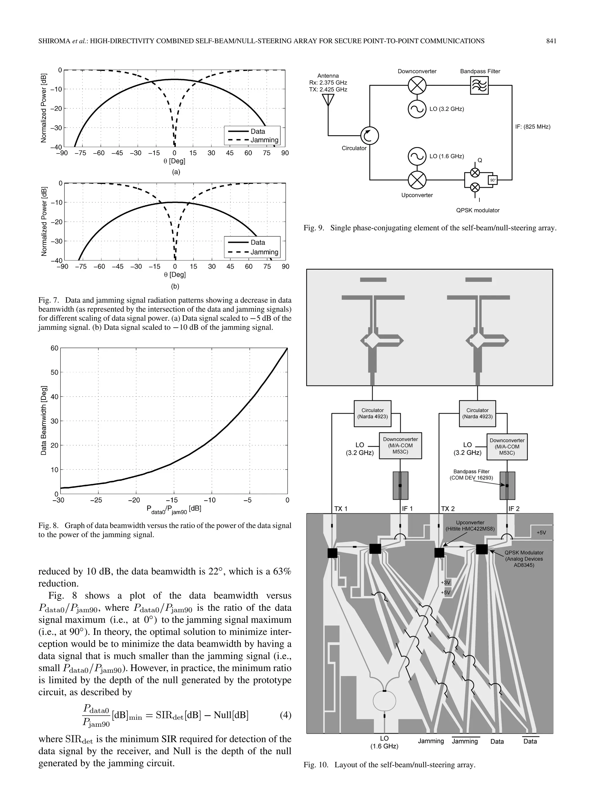
![842 IEEE TRANSACTIONS ON MICROWAVE THEORY AND TECHNIQUES, VOL. 55, NO. 5, MAY 2007
Fig. 11. Measurement setup for the BER versus receive angle () radiation
patterns. For the radiation patterns of the data and jamming signals, the receive
antenna is connected directly to the spectrum analyzer.
Fig. 12. Digital oscilloscope sample of the recovered baseband signal con-
taining both the data and jamming signals.
III. SELF-STEERING ARRAY IMPLEMENTATION
A high-directivity self-steering array is realized by inte-
grating the beam/null transmit array with a phase-conjugating
circuit. Fig. 9 shows a schematic of the phase-conjugating
element, which is achieved through a dual-mixing process, as
in [14] and [15]. The layout of the two-element self-beam/null-
steering array is shown in Fig. 10.
The 2.375-GHz interrogating signal is received by an -band
quasi-Yagi antenna connected to a Narda 4923 circulator that
allows both the transmit and receive circuits to share one an-
tenna. The -band quasi-Yagi antenna is a 2 : 1 scaled version
of the -band design described in [16]. The received signal then
passes through a M/A-COM M53C downconverting mixer, fol-
lowed by a COM DEV 162963 surface acoustic wave bandpass
filter.
The 2.375-GHz RF signal contains a geometry phase de-
pending on the direction of the interrogator. By choosing an
LO frequency of 3.2 GHz, which is higher than the frequency
of the RF signal, the resulting 825-MHz IF signal will contain a
conjugate of the original geometry phase. Since the phase-con-
jugated IF signal is then applied to the transmit beam/null
array, the direction of the beam/null will be steered towards the
direction of the interrogator.
The modulator is an Analog Devices AD8345 quadrature
modulator. The modulated signal is upconverted (Hittite
Fig. 13. Measurement setup for the bistatic radiation patterns. The interrogator
horn is fixed at 0 , +20 , and 010 , while a second receive horn is swept from
060 60 .
Fig. 14. Radiation patterns with interrogator fixed at = 0 . (a) Data and
jamming signals. (b) SIR. (c) BER.
HMC422MS8) to 2.425 GHz and passes through the circulator
to the antenna. The bandpass filter prevents any leakage of the
2.425-GHz transmit signal from passing through the downcon-
verter and entering the modulator.
For the prototype circuit, both elements are fabricated on
a single layer of Rogers Duroid 6010 (thickness: 0.635 mm,
). Wilkinson power dividers are used to split the up-
converting and downconverting LO signals between the two ele-
ments. The quasi-Yagi antennas are fabricated on Rogers Duroid
6010 (thickness: 2.54 mm, ).](https://image.slidesharecdn.com/15486473-250612061438-3db84195/75/Ieee-Mttv055i05-200705-05th-Edition-Fantomasping-37-2048.jpg)
![SHIROMA et al.: HIGH-DIRECTIVITY COMBINED SELF-BEAM/NULL-STEERING ARRAY FOR SECURE POINT-TO-POINT COMMUNICATIONS 843
Fig. 15. Radiation patterns with interrogator fixed at = 010 . (a) Data and
jamming signals. (b) SIR. (c) BER.
IV. MEASUREMENT AND RESULTS
Fig. 11 shows the measurement setup used to test the proto-
type self-beam/null steering array. The 2.375-GHz interrogator
signal is provided by a signal generator (Hewlett-Packard
E4433B) connected to a horn antenna. The interrogator is
received by the self-beam/null-steering array and retransmitted
at 2.425 GHz with the information and jamming data. The
information data is generated by the BERT (Tektronics PB200),
while a separate BERT transmitter (Tektronics GB1400T) is
used to generate the jamming data. A second horn antenna
receives the 2.425-GHz signal from the test array, where
it is amplified by a low-noise amplifier (L3 Microwave,
DBL-0218N308-2MH), followed by a true-time-delay phase
shifter [17] (based on M/A-Com MA46505-1088 varactor
diodes). A downconverting mixer (Hittite HMC-422MS8G),
low-pass filter, and noninverting amplifier are used to demod-
ulate the received signal and send the information data back
to the BERT. The phase shifter is used to control the phase of
the received signal so that it is in-phase with the LO signal,
which allows for maximum baseband signal amplitude during
demodulation. This is done by using a digital oscilloscope (HP
54503A) to monitor the demodulated signal so that the phase
shifter can be adjusted for maximum performance.
Fig. 12 shows a sample of the recovered baseband signal from
the digital oscilloscope. In this case, the recovered signal con-
tains a component of both the data and jamming signal.
Fig. 16. Radiation patterns with interrogator fixed at = +20 . (a) Data and
jamming signals. (b) SIR. (c) BER.
The self-steering properties of the array is confirmed through
a bistatic radiation pattern measurement. In the bistatic mea-
surement, the position of the 2.375-GHz interrogating horn is
fixed, while a second receiving horn is mounted on a computer-
controlled rotational arm, measuring the 2.435-GHz signal from
(Fig. 13). Bistatic measurements were con-
ducted for interrogating angles of 0 , 20 , and 10 .
Fig. 14(a) shows the radiation patterns of the information
and jamming signals when an interrogator is placed at
. This measurement is performed by connecting the receive
horn directly to a spectrum analyzer, as shown in Fig. 11. By
using a “1010 ” type string at a slightly different data rate
for the data and jamming signals, each spectrum may be in-
dependently observed on the spectrum analyzer. The measure-
ments clearly show both beam and null are self-steered toward
the interrogator, effectively pointing the peak of the SIR at the
interrogator.
The prototype circuit produced a jamming signal with a null
depth of 25 dB. According to (4), for an SIR of 20 dB, the power
of the data signal should be scaled to 5 dB of the jamming
signal and would result in a data beamwidth of 40 (Fig. 8).
Fig. 14(b) shows the SIR versus the observation angle, which is
calculated based on the measured radiation patterns. Due to the
high directivity of the null, the SIR pattern has a much higher
directivity than a conventional two-element array. Fig. 14(c)
shows the BER versus the observation angle. As expected, the
information was only recovered between angles of 20 .](https://image.slidesharecdn.com/15486473-250612061438-3db84195/75/Ieee-Mttv055i05-200705-05th-Edition-Fantomasping-38-2048.jpg)
![844 IEEE TRANSACTIONS ON MICROWAVE THEORY AND TECHNIQUES, VOL. 55, NO. 5, MAY 2007
The radiation patterns when the interrogator is placed at 10
and 20 are shown in Figs. 15 and 16. For interrogation angles
of 0 , 10 , and 20 , interception is disabled 20 from the
direction of the interrogator.
V. CONCLUSION
A high-directivity self-beam/null-steering array was intro-
duced for secure point-to-point BPSK modulation. The null and
beam arrays were successfully combined into one single-layer
array using QPSK modulators. The two-element 2.4-GHz pro-
totype shows high SIR directivity, while BER measurements
confirm that interception is disabled 20 from the direction
of the interrogator.
ACKNOWLEDGMENT
The authors would like to thank E. Taketatsu and N. W. Karo,
both with Pipeline Communications and Technology Inc., Hon-
olulu, HI, for valuable discussions.
REFERENCES
[1] J.-I. Takada, K. Sakaguchi, S. Suyama, K. Araki, M. Hirose, and M.
Miyake, “A super resolution spatio-temporal channel sounder for fu-
ture microwave mobile communication system development,” in IEEE
APCCAS Dig., Nov. 1998, pp. 101–104.
[2] Y. Sanada, J.-I. Takdada, and K. Araki, “A novel cumulant based
MUSIC like DOA estimation algorithm with multicarrier modulation,”
IEICE Trans. Commun., vol. E81-B, no. 12, pp. 2318–2325, Dec.
1998.
[3] M. Tangemann and R. Rheinschmitt, “Comparison of upgrade
techniques for mobile communication systems,” in IEEE SUPER-
COMM/ICC Dig., 1994, pp. 201–205.
[4] S.-S. Jeon, Y. Wang, Y. Qian, and T. Itoh, “A novel smart antenna
system implementation for broadband wireless communications,”
IEEE Trans. Antennas Propag., vol. 50, no. 5, pp. 600–606, May 2002.
[5] C. Uhlik and M. Dogan, “Antenna array for point-to-point microwave
radio system,” U.S. Patent 7 027 837, Apr. 11, 2006.
[6] R. Y. Miyamoto, G. S. Shiroma, and W. A. Shiroma, “A high-direc-
tivity transponder using self-steering arrays,” in IEEE MTT-S Int. Mi-
crow. Symp. Dig., Fort Worth, TX, Jun. 2004, pp. 1683–1686.
[7] R. Miyamoto, W. Shiroma, G. Shiroma, B. Murakami, A. Ohta, and
M. Tamamoto, “Microwave self-phasing antenna arrays for secure data
transmission and satellite network crosslinks,” U.S. Patent 7 006 039,
Feb. 28, 2006.
[8] H. Steyskal, R. Shore, and R. Haupt, “Methods for null control and
their effects on the radiation pattern,” IEEE Trans. Antennas Propag.,
vol. AP-34, no. 3, pp. 404–409, Mar. 1986.
[9] H. Steyskal, “Simple method for pattern nulling by phase perturbation,”
IEEE Trans. Antennas Propag., vol. AP-31, no. 1, pp. 163–166, Jan.
1983.
[10] ——, “Synthesis of antenna pattern with prescribed nulls,” IEEE Trans.
Antennas Propag., vol. AP-30, no. 3, pp. 273–279, Mar. 1982.
[11] T. Vu, “Simultaneous nulling in sum and difference patterns by ampli-
tude control,” IEEE Trans. Antennas Propag., vol. AP-34, no. 2, pp.
214–218, Feb. 1986.
[12] T. Ismail, “Null steering in phased arrays by controlling the element po-
sition,” IEEE Trans. Antennas Propag., vol. 39, no. 11, pp. 1561–1566,
Nov. 1991.
[13] D. Goshi, K. M. K. H. Leong, and T. Itoh, “A retrodirective array with
interference rejection capability,” in IEEE MTT-S Int. Microw. Symp.
Dig., Long Beach, CA, Jun. 2005, pp. 395–398.
[14] D. K. M. Skolnik, “Self-phasing array antennas,” IEEE Trans. An-
tennas Propag., vol. 12, no. 3, pp. 142–149, Mar. 1964.
[15] L. D. DiDomenico and G. M. Rebeiz, “Digital communications using
self-phased arrays,” IEEE Trans. Microw. Theory Tech., vol. 49, no. 4,
pp. 677–684, Apr. 2001.
[16] C. Ha, Y. Qian, and T. Itoh, “A modified quasi-Yagi planar antenna
with wideband characteristics in C-band,” in IEEE AP-S Int. Symp.
Dig., Jul. 2001, pp. 154–157.
[17] A. S. Nagra and R. A. York, “Distributed analog phase shifters with
low insertion loss,” IEEE Trans. Microw. Theory Tech., vol. 47, no. 9,
pp. 1705–1711, Sep. 1999.
Grant S. Shiroma (S’00) received the B.S. and M.S. degrees in electrical engi-
neering from the University of Hawaii at Manoa, in 2002 and 2004, respectively,
and is currently working toward the Ph.D. degree in electrical engineering at the
University of Hawaii at Manoa.
His research interests include microwave circuits and phased arrays.
Mr. Shiroma is a member of the 2007 IEEE Microwave Theory and Tech-
niques Society (IEEE MTT-S) International Microwave Symposium (IMS)
Steering Committee. He was the recipient of the 2004 IEEE MTT-S Graduate
Fellowship Award.
Ryan Y. Miyamoto (S’97–M’03) received the B.S. degree in physical elec-
tronics from the Tokyo Institute of Technology, Tokyo, Japan, in 1997, and the
M.S. and Ph.D. degrees in electrical engineering from the University of Cali-
fornia at Los Angeles, in 1999 and 2002, respectively.
He is currently a Senior RF Research Engineer with Oceanit Laboratories
Inc., Honolulu, HI, where he has been involved with development of phased
arrays for on-the-move satellite communications. Prior to joining Oceanit Lab-
oratories Inc., he was with the University of Hawaii at Manoa. He has authored
or coauthored over 30 technical publications in refereed journals and conference
proceedings. He holds one U.S. patent. His research interests include phased ar-
rays, smart antennas, and radar systems.
Dr. Miyamoto is currently an area editor for IEEE Microwave Magazine. He
was a recipient of the 2000 International Symposium on Antennas and Propa-
gation (ISAP) Award.
Justin D. Roque (S’04) received the B.S. and M.S.
degrees in electrical engineering from the University
of Hawaii at Manoa, in 2004 and 2006, respectively.
He is currently with the Intermediate Maintenance
Facility, Pearl Harbor Naval Shipyard, Honolulu, HI.
His research interests include microwave circuits and
phased arrays.
Mr. Roque is a member of the 2007 IEEE Mi-
crowave Theory and Techniques Society (IEEE
MTT-S) International Microwave Symposium (IMS)
Steering Committee.
Joseph M. Cardenas (S’04–M’06) received the B.S.
degrees in electrical engineering from the University
of Hawaii at Manoa, in 2005.
He is currently an RF Electrical Engineer with
Oceanit Laboratories Inc., Honolulu, HI, where
he has been involved with development of phased
arrays for on-the-move satellite communications.
His research interests include microwave circuits,
phased arrays, and nanosatellites.
Mr. Cardenas is a member of the 2007 IEEE
Microwave Theory and Techniques Society (IEEE
MTT-S) International Microwave Symposium (IMS) Steering Committee.
Wayne A. Shiroma (S’85–M’87) received the B.S.
degree from the University of Hawaii at Manoa, in
1986, the M.Eng. degree from Cornell University,
Ithaca, NY, in 1987, and the Ph.D. degree from the
University of Colorado at Boulder, in 1996, all in
electrical engineering.
In 1996, he joined the University of Hawaii at
Manoa, where he is currently an Associate Professor
of electrical engineering and Co-Director of the
Hawaii Space Flight Laboratory. He also served
as a Member of the Technical Staff with Hughes
Space and Communications, El Segundo, CA. His research interests include
microwave circuits and antennas.
Dr. Shiroma is a member of the IEEE MTT-S Administrative Committee and
General Chair of the 2007 IEEE Microwave Theory and Techniques Society
(IEEE MTT-S) International Microwave Symposium (IMS).](https://image.slidesharecdn.com/15486473-250612061438-3db84195/75/Ieee-Mttv055i05-200705-05th-Edition-Fantomasping-39-2048.jpg)
![IEEE TRANSACTIONS ON MICROWAVE THEORY AND TECHNIQUES, VOL. 55, NO. 5, MAY 2007 845
Polar SiGe Class E and F Amplifiers Using
Switch-Mode Supply Modulation
Jennifer N. Kitchen, Student Member, IEEE, Ilker Deligoz, Student Member, IEEE, Sayfe Kiaei, Fellow, IEEE, and
Bertan Bakkaloglu, Member, IEEE
Abstract—Two integrated polar supply-modulated class E and F
power amplifiers (PAs) in 0.18- m SiGe BiCMOS process are pre-
sented. The amplifiers are used to transmit GSM-EDGE signals
with an envelope dynamic range of 11 dB and a frequency range
of 880–915 MHz. The amplifiers use switch-mode dc–dc buck con-
verters for supply modulation, where sigma–delta (61 ), delta
(1 ), and pulsewidth modulation are used to modulate the PA
amplitude signal. A framework has been developed for comparing
the three switching techniques for EDGE implementation. The
measurement results show that 1 gives the highest efficiency
and lowest adjacent channel power, providing class E and F PA
efficiencies of 33% and 31%, respectively, at maximum EDGE
output power. The corresponding class E and F linearized am-
plifiers’ output spectra at 400-kHz offset are 54 and 57 dBc,
respectively.
Index Terms—EDGE, polar modulation, power amplifiers (PAs),
switching amplifiers.
I. INTRODUCTION
DUE TO the increasing demand for higher data rate wireless
access and the limitations on wireless frequency bands,
various linear modulation schemes such as multilevel quadra-
ture amplitude modulation (QAM) and phase-shift keying
(PSK) are being utilized to maximize bandwidth efficiency.
Linear modulation schemes assign each symbol on the constel-
lation with a unique phase and amplitude, thus requiring linear
power amplifiers (PAs) to transmit the signal. The inherent
disadvantage with linear PAs is low operating efficiencies,
where the efficiency decreases at backed-off powers. Since
PAs are operating at backed-off power most of the time, due to
the input signal’s high peak-to-average ratio and variable RF
transmitter power control, increasing the PA efficiency over a
range of operating powers improves the battery life in wireless
handsets [1].
Polar modulation, illustrated in Fig. 1, and its variations are
gaining momentum as potential methods to increase the ampli-
fier efficiency over a wide range of output powers while main-
taining linearity [2], [3]. In a polar PA, the phase and amplitude
information of the RF input signal are calculated from its Carte-
sian coordinates and independently processed through the am-
Manuscript received August 10, 2006; revised December 12, 2006. This work
was supported in part by the National Science Foundation under a Graduate
Fellowship and by the Connection One Research Center.
The authors are with the Connection One Research Center, Department
of Electrical Engineering, Arizona State University, Tempe, AZ 85287 USA
(e-mail: Jennifer.Desai@asu.edu).
Digital Object Identifier 10.1109/TMTT.2007.895407
plifier. The RF voltage signal is described by its in-phase
and quadrature baseband components as
The input signal can also be represented in polar coordinates as
(1)
where the RF signal’s amplitude and phase are
and
The RF modulated phase signal is typically processed through
the input of a nonlinear high-efficiency PA, while the enve-
lope information modulates the PA’s supply and/or bias voltage.
Linear low-dropout (LDO) regulators and switch-mode dc–dc
converters can be used for the PA supply modulation [3]–[5]. In
a more recent study, combined linear and switch-mode regulator
topologies are used to improve supply modulator efficiency and
linearity [6].
This paper presents two integrated SiGe switch-mode
supply-modulated class E and class F PAs for RF linear
transmitters. The highlights of the two amplifier architectures
are: 1) monolithic implementation of the switch-mode supply
modulator and switch-mode PA and 2) digital noise-shaping
supply modulator to increase PA efficiency and minimize the
effect of modulator switching noise on the PA performance.
In this paper, sigma-delta modulation ( ), delta modu-
lation ( ), and pulsewidth modulation (PWM) are used
to modulate the PA supply using the input signal’s envelope
information . The key advantage of using a digital con-
troller is programmability and flexibility in testing various
switching schemes. The amplifiers are integrated on a 0.18- m
SiGe BiCMOS process and transmit eight phase–shift keying
(8PSK) signals for potential use with the EDGE standard at
frequencies between 880–915 MHz. Section II introduces de-
tails of the amplifier architectures. The three digital modulation
schemes used to control the supply modulator are compared
in Section III. System implementation for EDGE modulation
is considered in Section IV, and design considerations for the
class E and F PAs are discussed in Section V. Section VI shows
measurement results for the class E and F amplifier topologies,
and conclusions are presented in Section VII.
0018-9480/$25.00 © 2007 IEEE](https://image.slidesharecdn.com/15486473-250612061438-3db84195/75/Ieee-Mttv055i05-200705-05th-Edition-Fantomasping-40-2048.jpg)
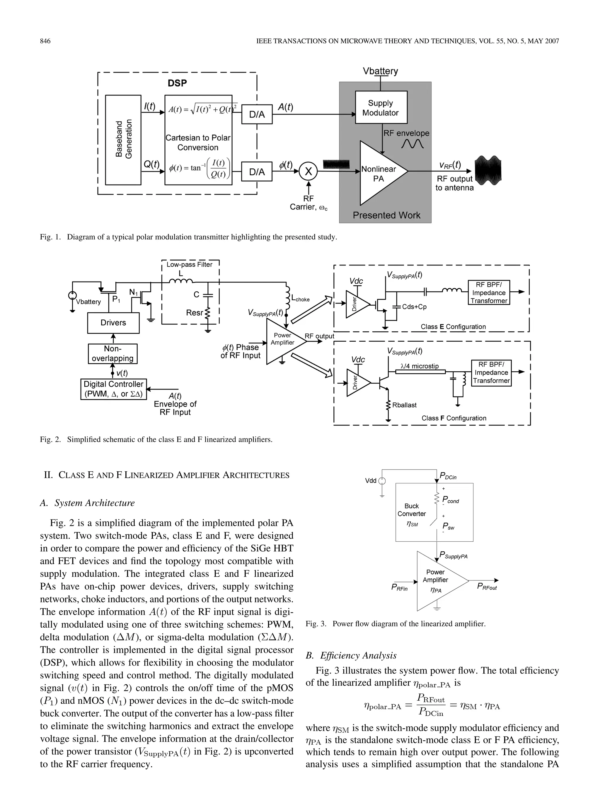
![KITCHEN et al.: POLAR SiGe CLASS E AND F AMPLIFIERS USING SWITCH-MODE SUPPLY MODULATION 847
efficiency is constant at backed-off output powers. The supply
modulator efficiency is described as
(2)
where is the PA output power, is the total con-
duction loss in the switch-mode buck converter, and is the
total converter switching loss. The conduction losses are depen-
dent on the PA output power, whereas the switching losses re-
main constant over output power for a fixed converter switching
speed. The efficiency of the presented topology can be esti-
mated over varying output powers given a known maximum
supply modulator efficiency of at a maximum PA RF
output power of . The switch-mode buck converter
is assumed to be optimally designed for equal conduction and
switching loss at the maximum RF output power .
By substituting and into (2), the converter
losses are estimated as
where is the duty ratio of the supply switching network, which
is related to the RF output power , as
Therefore, the efficiency of the linear amplifier is found as
(3)
In Fig. 4, the amplifier efficiency is plotted with
respect to output power for constant switch-mode PA efficiency
of 60% and maximum buck converter efficiency
of 90%. Assuming that the majority of the standalone PA losses
are due to the power device, the polar PA can be compared with
an implementable class B PA having a maximum efficiency of
60%. When comparing the two amplifiers in Fig. 4, the polar
PA shows up to a 17% improvement in efficiency at backed-off
powers.
III. SUPPLY MODULATOR SWITCHING SCHEMES
In this study, three digital modulation schemes have been
used to control the switching supply modulator, namely:
1) PWM; 2) sigma-delta ( ); and 3) delta ( )
modulation.
A. Pulsewidth Modulator
Most of the state-of-the-art switch-mode converters are con-
trolled using the PWM technique, as it provides high switching
Fig. 4. Theoretical efficiency versus output power levels of the presented polar
PA and a class B PA with 60% maximum efficiency.
Fig. 5. (a) PWM generator block diagram. (b) Critical waveforms.
efficiency and a low noise floor. One of the major disadvantages
of PWM is high harmonic content at integer multiples of its op-
erating frequency. As shown in Fig. 5(a), in a PWM controller,
the output switching waveform is created by com-
paring the ramp voltage to the input signal voltage .
As shown in Fig. 5(b), duty cycle of the switching waveform
is proportional to the amount of time that the ramp voltage is
higher than the input voltage.
The spectrum of an ideal PWM waveform can be found for
a dc input voltage by approximating the PWM switching wave-
form with a train of pulses with a pulsewidth of , where
is the period of the ramp voltage. For a maximum ramp voltage
equal to , the output of the PWM modulator with
a dc input can be approximated by [7]](https://image.slidesharecdn.com/15486473-250612061438-3db84195/75/Ieee-Mttv055i05-200705-05th-Edition-Fantomasping-42-2048.jpg)

![KITCHEN et al.: POLAR SiGe CLASS E AND F AMPLIFIERS USING SWITCH-MODE SUPPLY MODULATION 849
Fig. 9. 61M input (sinusoid) and output transient waveforms for a 100-kHz
input signal frequency and 5-MHz clock frequency.
comparator acting as a single-bit quantizer. can be de-
scribed in the discrete time domain with a sampling period of
as follows:
where is the white quantization noise introduced by the
single-bit quantizer. The -domain representation of the above
equation is modeled in Fig. 8(b) and found as [8]
(6)
Converting (6) to its frequency-domain representation and
calculating the PSD of the output gives [8]
(7)
where is the clock frequency controlling the input
sampling rate, and the PSD of the white noise in the single-bit
quantizer can be shown as
(8)
Equation (7) reveals that the ’s output signal power
is the input signal power with added quantization noise power
described by the second term. shapes the quantization
noise power of the quantizer out to higher frequencies with
the highest noise density from the modulator occurring at
. Fig. 9 shows an example of the transient output
for a 5-MHz clock frequency and 100-kHz sinusoidal input
with 3.3-V peak-to-peak voltages. Fig. 10 simulates the power
spectrum at the output of the digital ( in Fig. 2) for
the sinusoidal input signal shown in Fig. 9. Although
has a higher noise floor than the PWM, it does not create high
tonal power and the noise remains below 25 dBc from the
fundamental frequency power.
C. Delta ( ) Modulator
Another noise-shaping technique, illustrated in Fig. 11, is
delta modulation ( ), which is based on predictive quanti-
Fig. 10. 61M output spectrum for a 100-kHz sinusoidal input voltage and
5-MHz clock frequency. (a) Spectrum up to 17.5 MHz. (b) Zoomed-in spectrum
up to f =2.
Fig. 11. 1M block diagram.
zation [9]. This work implements using a low-pass filter
within the modulator feedback loop. The difference between the
input signal ( ) and the filtered output signal is quantized
using a comparator acting as a single-bit quantizer. can be
described in the discrete time domain as
where is the white quantization noise, is the com-
parator gain, and is the impulse response of the
low-pass filter in the feedback path. Assuming a first-order But-
terworth filter in the feedback loop, the PSD of the output
up to is estimated as](https://image.slidesharecdn.com/15486473-250612061438-3db84195/75/Ieee-Mttv055i05-200705-05th-Edition-Fantomasping-44-2048.jpg)
![850 IEEE TRANSACTIONS ON MICROWAVE THEORY AND TECHNIQUES, VOL. 55, NO. 5, MAY 2007
Fig. 12. 1M input (sinusoid) and output transient waveforms for a 100-kHz
input signal frequency and 5-MHz clock frequency.
(9)
where is the Butterworth filter 3-dB corner frequency, is
the Butterworth filter passband gain, and is described
by (8). The comparator gain is inherently large because the
feedback signal closely tracks the envelope signal , thus
producing a small error signal at the comparator’s input. For
a Butterworth filter passband gain of 1, the first term of
(9) approaches unity at frequencies much lower than , thus
giving a output power equal to the input signal power with
added quantization noise power. shapes the quantization
noise power of the single-bit quantizer out to higher frequencies
with the high-pass response described by the second term of (9).
The maximum noise density is approximately equal to the white
quantization noise density of (8) at .
Fig. 12 shows an example of the transient output for
a 5-MHz clock frequency and 100-kHz sinusoidal input with
3.3-V peak-to-peak voltages. Fig. 13 simulates the power spec-
trum at the output of the digital ( in Fig. 2) for the sinu-
soidal input signal shown in Fig. 12. Compared to ,
has a higher noise floor at frequencies close to the fundamental,
but has a slower noise floor increase with frequency. The
noise remains below 25 dBc from the fundamental power.
IV. SYSTEM IMPLEMENTATION FOR EDGE
EDGE E3/GSM 900 transmit requirements are summarized
in Table I [10]. The maximum EDGE output power of 23 dBm
produces an envelope signal described by the probability distri-
bution function (PDF) of Fig. 14, where the envelope reaches a
maximum value of 2.93 V and an rms voltage of approximately
2.0 V. Assuming a switch-mode class E/F PA efficiency of
50%, the buck (step-down) converter must have an output power
of 26 dBm (0.398 W) at the maximum EDGE PA output power.
Therefore, the effective output impedance of the buck converter
is calculated as
(10)
This value of is required in the following sections to find
the noise power of , , and PWM.
In order to compare the performance of , , and
PWM for supply modulators, a worst case noise analysis is
performed for each switching scheme. The most stringent PA
Fig. 13. 1M output spectrum for a 100-kHz sinusoidal input voltage and
5-MHz clock frequency. (a) Spectrum up to 17.5 MHz. (b) Zoomed-in spectrum
up to f =2.
TABLE I
EDGE E3/GSM 900 TRANSMITTER REQUIREMENTS
Fig. 14. EDGE envelope voltage distribution for the maximum PA output
power.
output spectrum specification for EDGE E3 has the spectral
mask shown in Fig. 15. At the lowest EDGE output power
of 5 dBm, the PA output PSD should fall below this mask.](https://image.slidesharecdn.com/15486473-250612061438-3db84195/75/Ieee-Mttv055i05-200705-05th-Edition-Fantomasping-45-2048.jpg)

![852 IEEE TRANSACTIONS ON MICROWAVE THEORY AND TECHNIQUES, VOL. 55, NO. 5, MAY 2007
V. CIRCUIT IMPLEMENTATION
The two SiGe polar modulated amplifier designs use class E
and F switch-mode PAs with a switch-mode dc–dc buck con-
verter modulating the supply of the power device. The same
power train design and digital controller are used to generate
PWM, , and modulation for both PAs.
A. Class E Switch-Mode PA
The class E PA of Fig. 2 uses an n-FET device acting as
a power switch operating at 900 MHz in conjunction with a
lumped element output network to minimize the crossover of
output voltage and current waveforms [11]. When accounting
for finite drain inductance and monolithic implementation of the
PA, an additional capacitance was added in parallel with the
FET device in order to resonate with the on-chip choke inductor
value of 2.2 nH [12], [13]. The total width for the nMOS power
device is 4.5 mm, with a gate length of 0.18 m. The optimized
FET layout divides the total width into 625 fingers. Each unit
cell contains five gate fingers and is surrounded by substrate
contacts. Every five unit cell blocks are isolated using a deep
trench isolation ring.
The class E PA has a maximum output power of 26 dBm with
an efficiency of 55% at a constant supply voltage of 3.3 V. The
supply voltage is chosen as the maximum average voltage that
keeps the drain node below the breakdown voltage of the device.
The impedance transformer and a portion of the PA’s bandpass
output filter are applied off-chip to allow for flexibility in tuning.
B. Class F PA
The class F PA of Fig. 2 is designed with a supply voltage
applied to the collector of the HBT by an on-chip choke inductor
of 14 nH. An on-board transmission line and a shunt LC
network provide the class F operation [12]–[14]. The collector
voltage and current are shaped into square and half sine waves,
respectively, thus reducing the current–voltage overlap of the
transistor and increasing the efficiency. The class F PA input
power is chosen to provide switching-like operation of the HBT
power device.
The class F PA uses an HBT as the power transistor oper-
ating at a center frequency of 900 MHz with a measured peak
output power of 25.2 dBm and peak efficiency of 51% at a con-
stant 3.6-V supply voltage. The HBT unit cell is sized to have a
minimum saturation voltage while maintaining adequate cutoff
frequency. In order to satisfy the current density requirements
at high output power levels, the PA’s power device is created
from 125 parallel HBT unit cells with emitter ballasting to avoid
thermal runaway.
C. Switch-Mode Buck Supply Modulator
The switching supply modulator (Fig. 2) has a complemen-
tary pMOS ( ) and nMOS ( ) that allows for the supply to
switch from 3.3 V to ground. The and drivers are con-
trolled using digital , , or PWM modulators. The
buck converter gives approximately equal switching and con-
duction losses at a switching frequency of 30 MHz and a con-
verter load current of 240 mA. The efficiency of the converter
is approximately 81% at an output power level of 28 dBm with
a load current of 245 mA. The converter has a low-pass output
Fig. 17. Micrograph of the die.
filter with inductor and capacitor values of 820 nH and 2.2 nF,
respectively, which make an effective bandwidth of 3 MHz. The
filter’s self-resonant frequency, caused by component parasitics,
is greater than the PA output bandwidth and is compensated by
the PA output filter.
The chip is mounted in a quad flat no-lead (QFN) package
frame, as shown in Fig. 17, and the class E PA uses its output
bondwire inductances as part of its output filter network. The
switch-mode supply regulators’ active devices and drivers
are implemented on the same chip as the class E and F
switch-mode amplifiers, using deep trench isolation as well as
guard rings to minimize substrate bounce. The total chip area
is 2.1 mm 2.0 mm.
VI. MEASUREMENT RESULTS
A. Measured PA Efficiency
The output powers of the class E and F polar PAs are
controlled through their switch-mode supply modulators by
changing the duty cycle [denoted by in (3)] of the supply
modulator’s control waveform. The RF input power, which car-
ries the EDGE phase information, remains constant at 5 dBm.
The controller switching speed was held constant at 30 MHz.
The efficiency plots of Fig. 18 show the measured drain/col-
lector efficiency of the standalone switch-mode PA output stage
( ), as well as the power-added efficiency (PAE) of the entire
system ( ). The PAE includes losses associated with
the switch-mode buck converter, switch-mode PA, all drivers,
and the PA output filter and matching network.
B. Measured PA Linearity
The PAs were also characterized for linearity by measuring
their AM–PM and AM–AM distortion. The distortions are
measured with respect to the power supply voltage ( )
of the standalone class E/F PA using a constant RF input power
of 5 dBm. Fig. 19(a) shows the AM–PM distortion of the class
E and F amplifiers, which are measured over varying dc supply
voltage. Fig. 19(b) shows the measured AM–AM distortion
from the supply voltage to the RF output, which closely follows
an exponential relationship.
C. EDGE Measurements
The class F and E PAs were tested with EDGE E3 input sig-
nals. The maximum EDGE output powers produced by the class
F and E PAs are 22.2 and 23.5 dBm, respectively. Figs. 20 and 21
show the output spectrum adjacent channel power ratio (ACPR)](https://image.slidesharecdn.com/15486473-250612061438-3db84195/75/Ieee-Mttv055i05-200705-05th-Edition-Fantomasping-47-2048.jpg)
![KITCHEN et al.: POLAR SiGe CLASS E AND F AMPLIFIERS USING SWITCH-MODE SUPPLY MODULATION 853
Fig. 18. Measured efficiency versus output power of: (a) class F linearized am-
plifier and (b) class E linearized amplifier. Output power is obtained by changing
the duty cycle of the supply modulator control waveform.
Fig. 19. (a) Measured AM–PM distortion of class E/F PAs with respect to
power supply voltage (V ). (b) Measured AM–AM distortion char-
acterized by plotting PA output power with respect to power supply voltage
(V ).
at the 400- and 600-kHz offset frequencies for the class F and
E PAs at maximum EDGE output powers. The ACPR is mea-
sured with respect to the output signal carrier power and plotted
Fig. 20. Measured class F output spectrum at: (a) 400- and (b) 600-kHz offset
with respect to the switch-mode supply modulator operating frequency.
Fig. 21. Measured class E output spectrum at: (a) 400- (b) 600-kHz offset with
respect to the switch-mode supply modulator operating frequency.
with respect to supply modulator operating frequency. The mea-
surements are made using an -law compressed dynamic range
envelope signal of 11 dB [15]. The signal is compressed in
order to eliminate the effect of RF input signal feedthrough to](https://image.slidesharecdn.com/15486473-250612061438-3db84195/75/Ieee-Mttv055i05-200705-05th-Edition-Fantomasping-48-2048.jpg)
![854 IEEE TRANSACTIONS ON MICROWAVE THEORY AND TECHNIQUES, VOL. 55, NO. 5, MAY 2007
the output at low envelope voltages when the PAs power de-
vice has a low drain/collector voltage [3]. In order to compare
the PA performance with the EDGE linearity requirements, the
PA output signal is decompressed using the -law expansion
coefficients.
In order to achieve good linearity results, the PA output
signal’s envelope and phase information must be synchronized
with less than 40-ns misalignment in time. Therefore, a phase
equalizer delay of 30 ns is added to the baseband phase infor-
mation to achieve the optimum ACPR results. Since the supply
modulator low-pass filter bandwidth and the EDGE envelope
bandwidth remain constant, the delay compensation does not
change with the supply modulator operating frequency.
The theoretical analysis of Section IV concludes that the
output spectrum at the 400- and 600-kHz offsets should de-
crease with increasing supply modulator operating frequencies.
However, transient effects, such as finite rise and fall times
of the controller waveform, and increased converter distortion
at high frequencies may cause the ACPR to degrade at high
converter operating speeds. Moreover, the nonlinearities in the
standalone class E/F PAs contribute to ACPR degradation, as
well as high EVM results. The AM–PM distortion of Fig. 19(a)
verifies that the standalone PA causes phase distortion of the
RF input signal, and Fig. 19(b) shows that the PA output
amplitude loses its linear relationship to supply voltage around
0.9 V. Both of these nonidealities cause spectral spreading
at the polar PA output. As the PA output power decreases to
approximately 17 dBm, the ACPR at the 400- and 600-kHz
offsets degrades by 4 and 3 dB, respectively, for both the class
E and F PAs. For output powers below 17 dBm, the amplifiers
have an exponential degradation in linearity due to the high PA
AM–PM distortion and increased RF input signal feedthrough.
Since the standalone PAs operate within a limited supply
voltage dynamic range, the amplifiers do not meet the EDGE
specification over all power levels. The linearity at backed-off
power and the maximum achievable EDGE output power may
be increased by using power devices with higher breakdown
voltages. In order to improve linearity when using low supply
voltages, the feedthrough path from the PAs’ RF input signal to
the output should be eliminated.
The efficiencies of the class E and F polar PAs for EDGE
transmission are dependent upon the envelope regulator
switching scheme and operating frequency. The PAEs for ,
, and PWM versus digital controller operating frequency
are given in Fig. 22. The efficiencies are plotted for the max-
imum EDGE output power. Fig. 22(a) gives the class F results,
whereas Fig. 22(b) shows the class E results. As discussed
in Section IV, the digital controller operating frequency is
not necessarily equal to the buck converter power transistors’
average switching speed. Therefore, gives the highest
efficiency at high operating frequencies because its nominal
switching speed is around 30% of the operating frequency.
Using the operating frequencies calculated in Section IV, the
efficiency versus EDGE output power is plotted in Fig. 23 for
the three modulation schemes. These plots closely resemble the
predicted efficiencies of Fig. 16.
Table II summarizes the amplifiers’ EDGE measurement
results at maximum output power, including the peak error
Fig. 22. Measured PAE with respect to the switch-mode supply modulator op-
erating frequency for: (a) class F polar PA and (b) class E polar PA.
Fig. 23. Measured PAE versus EDGE output power for: (a) class F PA and
(b) class E PA.
vector magnitude (EVM) and rms error vector magnitude
(EVM-rms) measurements. The measurements are tabulated
for the switching frequencies that give the highest ACPR
performance.](https://image.slidesharecdn.com/15486473-250612061438-3db84195/75/Ieee-Mttv055i05-200705-05th-Edition-Fantomasping-49-2048.jpg)

![856 IEEE TRANSACTIONS ON MICROWAVE THEORY AND TECHNIQUES, VOL. 55, NO. 5, MAY 2007
and J. Griffiths and his team at Freescale Semiconductor Inc.,
for their technical support and HBT characterization.
REFERENCES
[1] P. B. Kenington, High-Linearity RF Amplifier Design. Norwood,
MA: Artech House, 2000.
[2] T. Sowlati et al., “Quad-band GSM/GPRS/EDGE polar loop trans-
mitter,” IEEE J. Solid-State Circuits, vol. 39, no. 12, pp. 2179–2189,
Dec. 2004.
[3] P. Reynaert and M. S. Steyaert, “A 1.75-GHz polar modulated CMOS
RF power amplifier for GSM-EDGE,” IEEE J. Solid-State Circuits, vol.
40, no. 12, pp. 2598–2608, Dec. 2005.
[4] D. K. Su and W. J. McFarland, “An IC for linearizing RF power ampli-
fiers using envelope elimination and restoration,” IEEE J. Solid-State
Circuits, vol. 33, no. 12, pp. 2252–2258, Dec. 1998.
[5] V. Yousefzadeh, N. Wang, Z. Popovic, and D. Maksimovic, “A
digitally controlled DC–DC converter for RF power amplifier,” IEEE
Trans. Power Electron., vol. 21, no. 1, pp. 164–172, Jan. 2006.
[6] N. Wang et al., “Linearity of X-band class-E power amplifiers in
EER operation,” IEEE Trans. Microw. Theory Tech., vol. 53, no. 3, pp.
1096–1102, Mar. 2005.
[7] Y. Shrivastava, S. Y. Hui, S. Sathiakumar, H. S.-H. Chung, and K.
K. Tse, “Harmonic analysis of nondeterministic switching models for
DC–DC power converters,” IEEE Trans. Circuits Syst. I, Fundam.
Theory Appl., vol. 47, no. 6, pp. 868–884, Jun. 2000.
[8] V. Comino, M. Steyaert, and G. Temes, “A first-order current-steering
sigma–delta modulator,” IEEE J. Solid-State Circuits, vol. 26, no. 3,
pp. 176–183, Mar. 1991.
[9] H. S. Black, Modulation Theory. New York: Van Nostrand, 1953.
[10] Digital cellular telecommunications system (phase 2+); radio trans-
mission and reception GSM 05.05. 1999, GSM 05.05 v 8.0.0.
[11] C. Li and Y. O. Yam, “Maximum frequency and optimum performance
of class E power amplifiers,” in Proc. IEEE Circuits Devices Syst., Jun.
1994, vol. 141, no. 3, pp. 174–184.
[12] J. D. Kitchen, I. Deligoz, S. Kiaei, and B. Bakkaloglu, “Linear RF polar
modulated SiGe class E and F power amplifiers,” in IEEE Radio Freq.
Integrated Circuits Symp., 2006, pp. 475–478.
[13] J. Desai, I. Deligoz, S. Kiaei, and B. Bakkaloglu, “Fully-integrated,
programmable, polar-modulated class E power amplifier,” in Wireless
Networks and Emerging Technol., Banff, AB, Canada, Jul. 2006, Paper
510-033.
[14] F. H. Raab, “Maximum efficiency and output of class-F power
amplifiers,” IEEE Trans. Microw. Theory Tech., vol. 49, no. 6, pp.
1162–1166, Jun. 2001.
[15] B. Sklar, Digital Communications: Fundamentals and Applications.
Englewood Cliffs, NJ: Prentice-Hall, 1988.
Jennifer N. Kitchen (S’00) received the B.S. degree
in electrical engineering from the University of Ari-
zona, Tucson, in 2002, the M.S. degree in electrical
engineering from Arizona State University, Tempe,
in 2005, and is currently working toward the Ph.D.
degree in electrical engineering at Arizona State
University.
In 2003 and 2004, she was a Summer Intern with
Freescale Semiconductor Inc. She is currently a Re-
search Assistant with Arizona State University. Her
research interests include efficiency enhancement
and linearization techniques for RF PAs in wireless transmitters.
Mrs. Kitchen is a National Science Foundation (NSF) Graduate Fellow. She
was a Semiconductor Research Corporation Master’s Scholar from 2003 to
2005.
Ilker Deligoz (S’98) was born in Amasya, Turkey, in
1979. He received the B.S. degree in electrical engi-
neering from Bilkent University, Ankara, Turkey, in
2002, the M.S. degree in electrical engineering from
Arizona State University, Tempe, in 2005, and is cur-
rently working toward the Ph.D. degree in electrical
engineering at Arizona State University.
From May 2003 to January 2004, he was an Intern
for the GSM RFIC Development Group, Intel Corpo-
ration, and in 2004, he was an Intern with Freescale
Semiconductor Inc., where he was involved with the
next-generation Cellular Power Amplifiers Research and Development Groups.
He is currently a Research Assistant with Arizona State University. His research
interests are RFIC and mixed-signal IC design for communication systems.
Sayfe Kiaei (S’86–M’87–SM’93–F’02) received the
Ph.D. degree in electrical engineering from Wash-
ington State University, Pullman, in 1987.
He is currently a Professor and the Director
of the Connection One Center (National Science
Foundation (NSF) Industry/University Cooperative
Research Center (I/UCRC) Center) and WINTech
Programs of the Ira A. Fulton School of Engineering,
Arizona State University, Tempe. From 1993 to
2001, he was a Senior Member of Technical Staff
with the Wireless Technology Center and Broadband
Operations, Motorola. From 1987 to 1993, prior to joining Motorola, he was
an Associate Professor at Oregon State University, where he taught courses
and performed research in digital communications, very large scale integration
(VLSI) system design, advanced CMOS IC design, and wireless systems. He
assisted in the establishment of the Industry–University Center for the Design
of Analog/Digital ICs (CDADIC) and served as a Co-Director of CDADIC
for ten years. He has authored or coauthored over 75 journal and conference
papers. He holds several patents. His research interests are wireless transceiver
design, and RF and mixed-signal ICs in CMOS and SiGe.
Bertan Bakkaloglu (M’94) received the Ph.D. de-
gree in electrical engineering from Oregon State Uni-
versity, Corvallis, in 1995.
He then joined the Mixed Signal Wireless Design
Group, Texas Instruments Incorporated, Dallas,
TX, where he was involved with analog, RF, and
mixed signal front-ends for wireless and wireline
communication ICs. He was also involved with
system-on-chip designs with integrated battery
management and RF and analog baseband func-
tionality as a design leader. In 2001, he joined the
Broadband Communications Group, Texas Instruments Incorporated, where he
was involved with cable modem analog front-end designs and gigabit Ethernet
front-ends. In 2004, he joined the Electrical Engineering Department, Arizona
State University, Tempe, as an Associate Professor. He holds three patents.
His research interests include RF and PA supply regulators, RF synthesizers,
high-speed RF data converters, and RF built-in-self-diagnostic circuits for
communication ICs and antennas.
Dr. Bakkaloglu has been a Technical Program Committee member for
the International Circuits and Systems Symposium (ISCAS) and Steering
Committee member for IEEE Microwave Theory and Techniques (MTT)/RFIC
conferences.](https://image.slidesharecdn.com/15486473-250612061438-3db84195/75/Ieee-Mttv055i05-200705-05th-Edition-Fantomasping-51-2048.jpg)
![IEEE TRANSACTIONS ON MICROWAVE THEORY AND TECHNIQUES, VOL. 55, NO. 5, MAY 2007 857
A 23-dBm 60-GHz Distributed Active Transformer
in a Silicon Process Technology
Ullrich R. Pfeiffer, Senior Member, IEEE, and David Goren, Member, IEEE
Abstract—In this paper, a distributed active transformer for the
operation in the millimeter-wave frequency range is presented.
The transformer utilizes stacked coupled wires as opposed to slab
inductors to achieve a high coupling factor of = 0 8at 60 GHz.
Scalable and compact equivalent-circuit models are used for the
transformer design without the need for full-wave electromagnetic
simulations. To demonstrate the feasibility of the millimeter-wave
transformer, a 200-mW (23 dBm) 60-GHz power amplifier has
been implemented in a standard 130-nm SiGe process technology,
which, to date, is the highest reported output power in an SiGe
process technology at millimeter-wave frequencies. The size of the
output transformer is only 160 160 m2 and demonstrates the
feasibility of efficient power combining and impedance transfor-
mation at millimeter-wave frequencies. The two-stage amplifier
has 13 dB of compressed gain and achieves a power-added ef-
ficiency of 6.4% while combining the power of eight cascode
amplifiers into a differential 100- load. The amplifier supply
voltage is 4 V with a quiescent current consumption of 300 mA.
Index Terms—Distributed active transformer (DAT), millimeter
wave, on-chip power combining, power amplifier (PA), silicon ger-
manium (SiGe), wireless communication.
I. INTRODUCTION
DISTRIBUTED active transformers (DATs) have recently
created some excitement at lower frequencies, e.g., around
2.4 GHz [1], [2], where the DAT topology promises highly effi-
cient, fully integrated, and watt-level power amplifiers (PAs) in
a standard low-voltage CMOS process technology. A fully in-
tegrated CMOS PA is one of the key building blocks that will
enable single-chip integrated transceivers in the future. Unlike
other power-combining techniques [3], [4], the DAT topology
provides power combining and efficient impedance transforma-
tion simultaneously to overcome the low transistor breakdown
voltage limitations that exist today.
Manuscript was received September 11, 2006; revised February 6, 2007. This
work was supported in part by the National Aeronautics and Space Administra-
tion under Grant NAS3-03070 and by the Defense Advanced Research Projects
Agency under Grant N66001-02-C-8014 and Grant N66001-05-C-8013.
U. R. Pfeiffer was with the IBM T. J. Watson Research Center, Yorktown
Heights, NY 10598 USA. He is now with the Terahertz Electronics Group, Insti-
tute of High-Frequency and Quantum Electronics, University of Siegen, 57068
Siegen, Germany (e-mail: ullrich@ieee.org).
D. Goren is with IBM Haifa Research Laboratories, Mount Carmel, Haifa
31905, Israel, and with the Technion, Israel Institute of Technology, Technion
City, Haifa 32000, Israel (e-mail: DAVIDG@il.ibm.com).
Color versions of one or more of the figures in this paper are available online
at http://ieeexplore.ieee.org.
Digital Object Identifier 10.1109/TMTT.2007.895654
Similarly, at millimeter-wave frequencies, faster bipolar
transistor technologies like silicon germanium (SiGe) HBTs
suffer the same breakdown voltage limitations due to their
continued device scaling [5], [6]. This makes high-power SiGe
amplifiers a crucial and challenging building block for many
millimeter-wave systems [7]. SiGe HBTs have achieved cutoff
frequencies as high as GHz [8], rivaling
the high-frequency performance of other III/V semiconductors
like InP-based HBTs. Potential applications for SiGe tech-
nologies are high-speed communications systems at 60 GHz
[9], [10] and beyond, as well as automotive radar systems at
77 GHz [11]. The breakdown voltages and of
today’s SiGe process technologies are typically below 2 and
6 V, respectively. For example, if one wants to deliver 23 dBm
(200 mW) from a single common-emitter device biased at 1.1 V
( V swing, V) into a 50- load, one would
need an impedance transformation ration of approximately
50 : 3 ( ); unlikely to be very efficient for
millimeter waves. Recent studies at 60 [7], [10], [12]–[14]
and 77 GHz [15], [16] have demonstrated single device output
powers as high as 15.5 dBm with a power-added efficiency
(PAE) typically lower than 10%. On-chip power combining and
balanced device operation has been exploited to enhance the
maximum available output power per chip (20 [17], 18.5 [16],
17.5 [18], and 21 dBm [19]).
This paper presents a 60-GHz DAT with a small area of
160 160 m . The transformer utilizes ground shielded and
stacked coupled wires as opposed to slab inductors to minimize
substrate induced losses and to achieve a high coupling factor
of . The DAT was used in a two-stage 60-GHz PA to
combine the power of four push–pull amplifiers in a standard
130-nm SiGe BiCMOS process technology. The amplifier de-
livers 200 mW (23 dBm) into a 100- differential load, which,
to date, is the highest reported output power in an SiGe process
technology at millimeter-wave frequencies. It has 13 dB of
compressed gain and achieves a PAE of 6.4%. Throughout
the design, scalable and compact equivalent circuit modeling
was used without iterative full-wave electromagnetic (EM)
simulations.
Section II describes the millimeter-wave design aspects of the
DAT, e.g., the transformer modeling, circuit architecture, and
tuning of the DAT for optimum efficiency. This includes a dis-
cussion of parasitic effects that have a considerable influence on
the symmetry of the DAT impedance transformation ratio, its
large-signal compression, and its stability. Section III describes
the experimental results showing the large-signal compression
of the PA in the 59–64-GHz frequency range. Finally, conclu-
sions from the results are drawn in Section IV.
0018-9480/$25.00 © 2007 IEEE](https://image.slidesharecdn.com/15486473-250612061438-3db84195/75/Ieee-Mttv055i05-200705-05th-Edition-Fantomasping-52-2048.jpg)
![858 IEEE TRANSACTIONS ON MICROWAVE THEORY AND TECHNIQUES, VOL. 55, NO. 5, MAY 2007
II. MILLIMETER-WAVE DAT
DATs, as described in [1], use two single-turn planar slab
inductors at 2.4 GHz to form a transformer where the primary
inductor is broken up into four quarter sections to facilitate
the connection of four synchronized push–pull amplifiers.
Each synchronized push–pull amplifier couples magnetically
to the same single turn primary inductor in such a way that
their alternating magnetic fluxes add constructively to form a
uniform circular current in the secondary winding. Since each
amplifier on the primary side utilizes only one quarter of the
primary inductor length, and not its full length, the impedance
transformation ratio is (1 : 4) instead of known
for a regular four-turn transformer.
Scaling the DAT topology from 2.4 GHz to millimeter-wave
frequencies imposes a series of challenges. Coplanar trans-
formers are typically used only at lower frequencies where
low coupling factors, substrate and skin effect losses, and
inaccuracies caused by model to hardware discrepancies can
be tolerated [2]. Monolithic on-chip transformers have been
widely used for matching and power-combining purposes in the
past up to a few tens of gigahertz, where the tuned circuits used
for matching have been formed by the transformer primary
inductances and additional capacitors to achieve the band-
width and efficiency required [20]. Commonly used on-chip
transformers are either made of inter-wound spiral inductors
or coplanar coupled wires (slab inductors) to promote mutual
magnetic coupling. In order to operate any transformer in the
millimeter-wave frequency range, its primary inductance has to
be reduced substantially, which, in turn, requires the values of
additional tuning capacitors to be extremely small. Therefore,
it is crucial to have a transformer or DAT structure that allows
accurate modeling and the prediction of parasitic effects. The
most important design challenges for millimeter-wave DATs
are: 1) the DAT requires well synchronized push–pull ampli-
fiers under all operating conditions to maintain the correct load
line impedance for each amplifier; 2) tuning of the DAT for
low loss and high efficiency requires accurate compact EM
modeling, as well as accurate parasitic extraction techniques;
and 3) nonidealities of the transformer such as its inter-winding
capacitance limit the scaling to higher frequencies and requires
optimized 1 : 1 transformer structures.
In the following, various design aspects of the DAT are de-
scribed. This includes a description of the transformer unit cell,
the DAT circuit architecture, a description of the input power
distribution network, the corner amplifier circuits, the compact
EM transformer modeling, the principle of active terminations,
the tuning of the DAT, parasitic effects at millimeter waves, as
well as scaling of the transformer to higher frequencies.
A. Transformer Unit Cell
Stacked transformers have an improved coupling factor on
silicon substrates than coplanar transformers. They can be ef-
fectively shielded from the lossy substrate with perpendicular
ground wires. Such wires do not allow longitudinal currents and,
therefore, do not change the inductance matrix and resulting
magnetic coupling [21], [22]. Stacked transformers can be used
for on-chip impedance transformation, power combining, RF
filters, and single-ended to differential conversion [23], [24].
Fig. 1. (a) Transformer cross section is shown with its primary and secondary
conductor above a ground shield. (b) 3-D view of the transformer from which
the ground shields perpendicular slots and side shields can be seen.
The transformer stack-up used in this paper is shown in
Fig. 1(a). The transformer is arranged in a “sandwich-like”
structure where the primary inductor is stacked vertically
above the secondary inductor. Both wires are located above
a ground shield and achieve a coupling factor of .
Fig. 1(b) shows a 3-D view of the transformer, which uses
a ground shield with perpendicular slots. To improve the
ability to predict the structures parasitic effects, side bars have
been added, which act as a well-defined return path, and a
closed environment EM condition for compact modeling at
millimeter-wave frequencies. Such modeling is scalable by
length and insensitive to close-by metal structures that may
be present dependent on the application and circuit layout,
an important feature that makes it a parametrized cell that
can be used in more complex DAT structures. Eight of these
identical unit cell transformers make up the full DAT structure,
as will be shown in Section II-B. The primary conductor uses
the 4- m-thick aluminum top metal layer (AM), whereas the
secondary conductor is on the 1.25- m-thick second aluminum
layer (LY). The ground shield with its slots orthogonal to wave
propagation and side bars collinear to wave propagation are on
a 0.5- m-thick copper layer (MQ). The transformer template
provides an extremely compact and optimized structure for
millimeter-wave operation. For example, its quality factor
for a 80- m-long transformer at 60 GHz is 32.
B. DAT Circuit Architecture
Fig. 2 shows a 3-D conceptual drawing of the DAT trans-
former structure. The simplified figure only shows the metal
shapes on the first three metal layers and omits the four dif-
ferential push–pull amplifiers in the corners for better clarity.
The DAT uses the thick top-level metal for the primary winding
and the second-level metal for the secondary winding. The dc
supply current for the push–pull amplifiers is supplied via a con-
nection in the center of the structure. A large via field in the
center connects a lower level 4-V power plane to ac grounds
in the center of the primary inductors on the top-level metal.
Note that the primary side is more susceptible to electromigra-
tion than the secondary side of the transformer since their pri-
mary inductor carries the amplifiers’ dc current in addition to its
primary RF current. The top-level metal is three times as thick](https://image.slidesharecdn.com/15486473-250612061438-3db84195/75/Ieee-Mttv055i05-200705-05th-Edition-Fantomasping-53-2048.jpg)
![PFEIFFER AND GOREN: 23-dBm 60-GHz DAT IN SILICON PROCESS TECHNOLOGY 859
Fig. 2. Conceptual 3-D drawing of the DAT physical structure.
as the second-level metal and is, therefore, the layer of choice
for the primary side, although the amplifiers’ signals have to go
all the way up through the metal stack to connect to the primary
inductors.
The millimeter-wave transformer requires its primary induc-
tance to be small to operate the DAT efficiently at millimeter-
wave frequencies. Its size is, therefore, only 160 160 m (see
Section II-G for the transformer tuning). Generally speaking,
a small transformer has some negative mutual magnetic cou-
pling between opposite sides of a wire loop since not all of the
magnetic flux can pass entirely through the center of the struc-
ture. This is primarily a problem in other, e.g., coplanar and
transformer structures, since it makes the 3-D EM modeling
dependent on the diameter and shape (square or circular) of a
transformer. As a result, one has to perform iterative 3-D EM
simulations to optimize the DAT geometry.
Unlike the coplanar DAT described in [1], [2], [25], and [26],
the millimeter-wave DAT transformer in this paper maximizes
the mutual magnetic coupling and simultaneously minimizes
the negative mutual induction to a point where it can be ne-
glected. The electrical performance of the DAT transformer
structure can, therefore, simply be modeled by the stacked
transformer templates described in Section II-A. A simplified
schematic of the DAT is shown in Fig. 3. Eight transformer
templates can be connected in series on the secondary winding
to form a single secondary turn. On the primary side, two
of them are connected to a 4-V supply (ac-ground) in the
center and the push–pull amplifiers at the opposite ends. The
ground shield with the slots orthogonal to wave propagation
and the side bars collinear to wave propagation are adapted
to accommodate the corners of the structure. The structure
maintains its closed environment EM condition, which relaxes
the parasitic effects and boundary conditions. The magnetic
flux is localized around the two wires so that only a small
amount of flux passes through the inner portion of the ring.
This provides the ability to use 2-D compact modeling, which
is scalable by length and independent of the proximity of other
structures in the layout (see Section II-E for EM modeling
of the transformer template). The transformer templates are
decoupled from each other, which allows them to be treated as
independent building blocks. This is specifically an important
feature at millimeter-wave frequencies where prior art coupled
line transformers require 3-D EM simulations for each circular
geometry.
The differential input signal to the four synchronized
push–pull amplifiers is pre-amplified by a pre-driver fol-
Fig. 3. Schematic of the DAT showing eight transformer templates and the
four differential push–pull amplifiers. A pre-driver followed by six inter-leaved
Wilkinson power splitters is used to create the phase matched inputs with alter-
nating polarity (not shown).
Fig. 4. Input power distribution network. Six inter-leaved Wilkinson power di-
viders are used to create the alternating phases for the corner amplifiers. The
signal path for the north–east amplifier (PA4) is highlighted here with the di-
vider sections in black and additional interconnects in gray.
lowed by six inter-leaved Wilkinson power splitters (see
Section II-C for more details). The impedance transforma-
tion ratio for an ideal DAT is , which
ideally creates a load line impedance for each amplifier of
. At millimeter-wave frequencies, the DAT,
however, is far from being ideal, which requires the reactive
part of the transformer to be tuned for an optimum load line and
coupling efficiency (see Sections II-G and H for more details).
C. Input Power Distribution Network
The input power distribution network is shown in Fig. 4. Six
equal-split Wilkinson power dividers (three for each polariza-
tion) are used to split the power from a differential driver am-
plifier in quarters. The network layout is inter-leaved to create](https://image.slidesharecdn.com/15486473-250612061438-3db84195/75/Ieee-Mttv055i05-200705-05th-Edition-Fantomasping-54-2048.jpg)


![This ebook is for the use of anyone anywhere in the United States
and most other parts of the world at no cost and with almost no
restrictions whatsoever. You may copy it, give it away or re-use it
under the terms of the Project Gutenberg License included with this
ebook or online at www.gutenberg.org. If you are not located in the
United States, you will have to check the laws of the country where
you are located before using this eBook.
Title: Captain Paul
Author: Alexandre Dumas
Release date: October 29, 2012 [eBook #41222]
Most recently updated: October 23, 2024
Language: English
Credits: Produced by David Widger
*** START OF THE PROJECT GUTENBERG EBOOK CAPTAIN PAUL
***](https://image.slidesharecdn.com/15486473-250612061438-3db84195/75/Ieee-Mttv055i05-200705-05th-Edition-Fantomasping-60-2048.jpg)