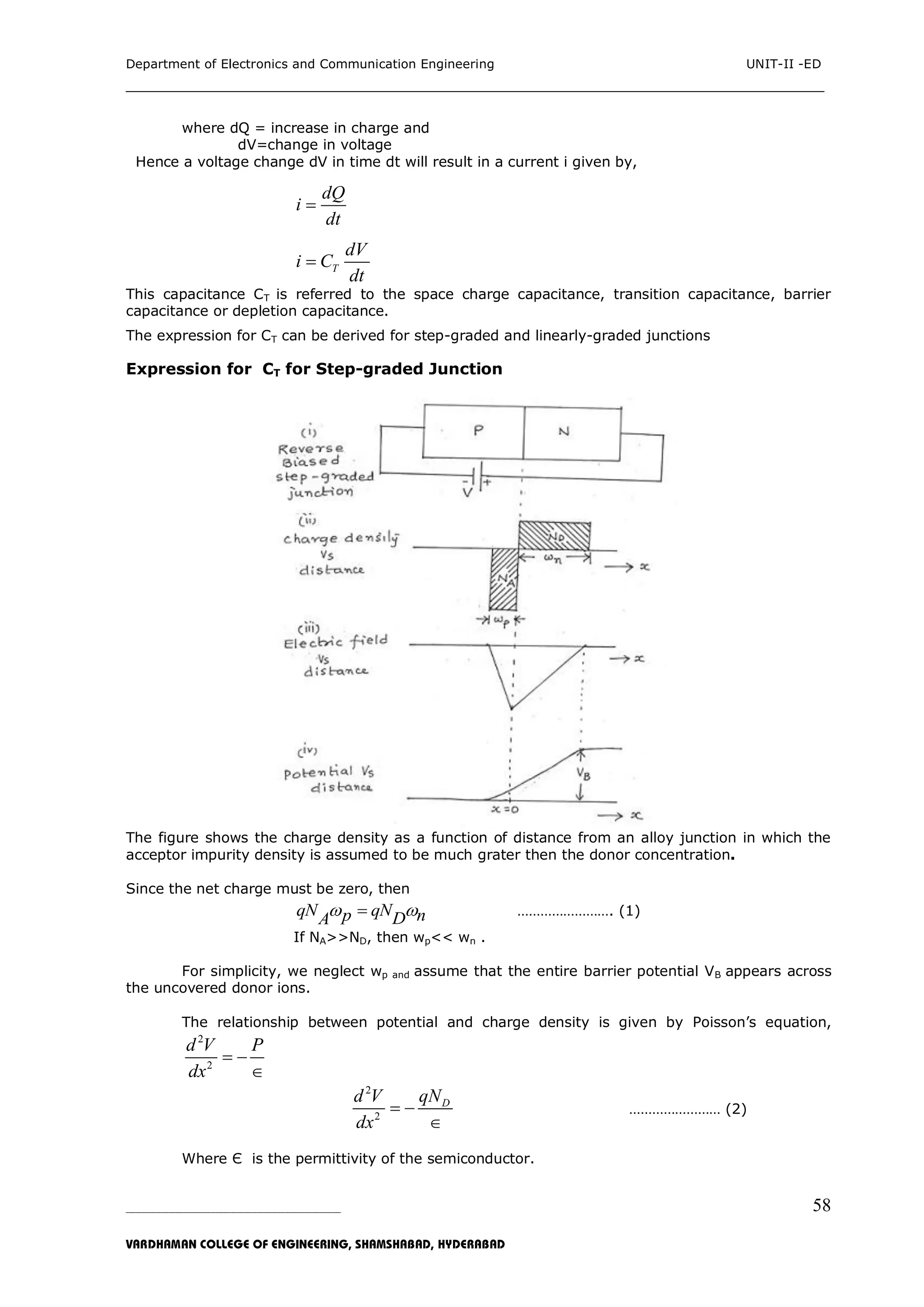
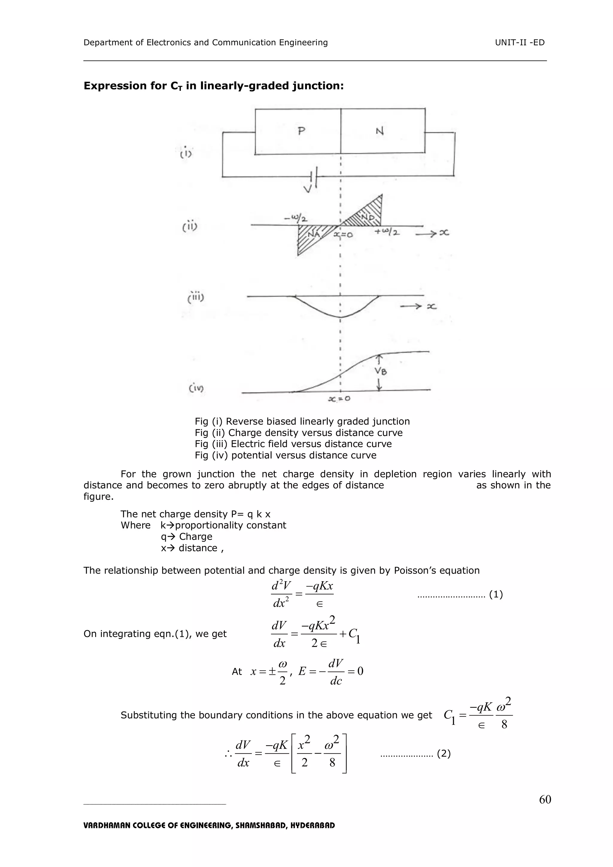
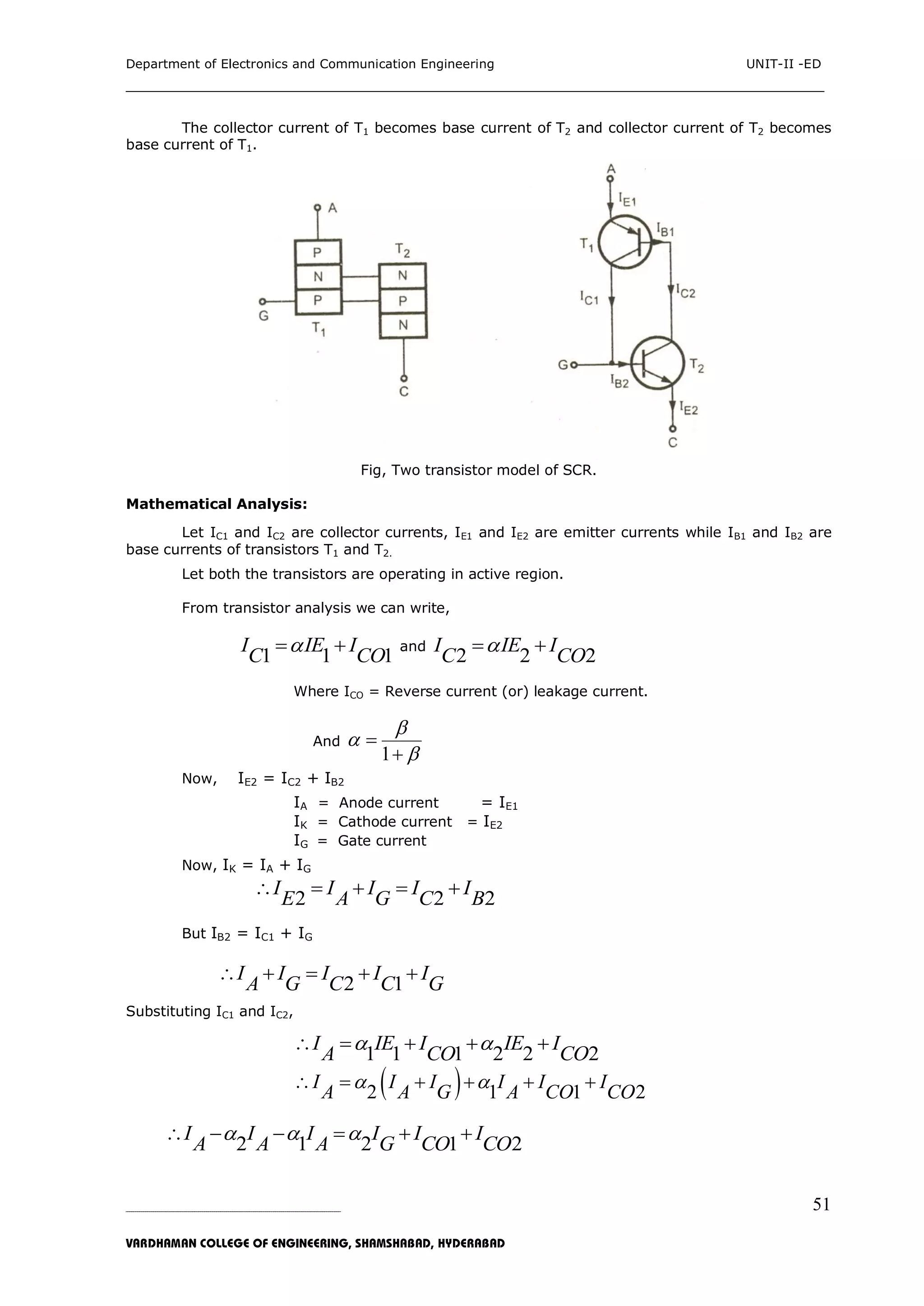
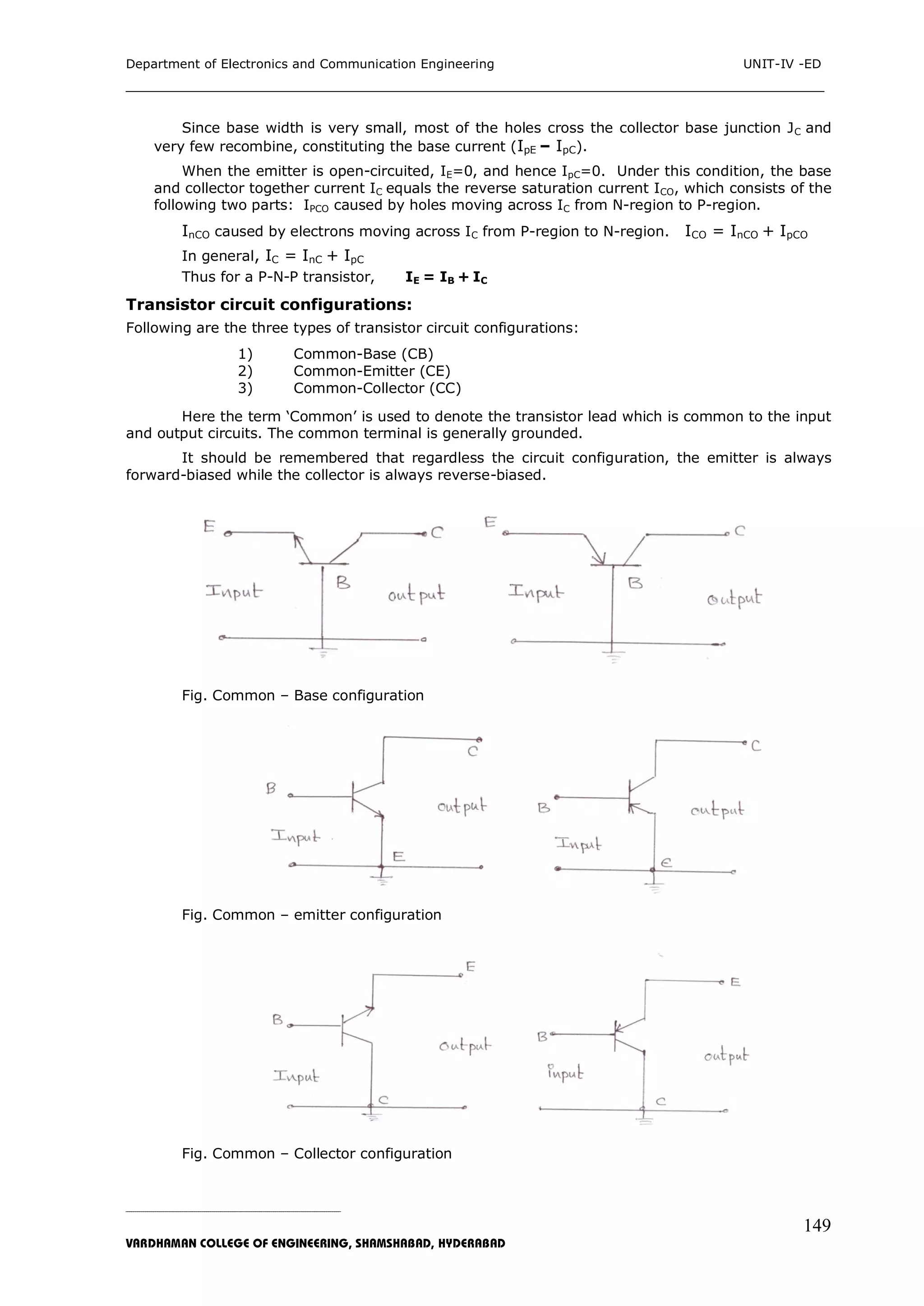
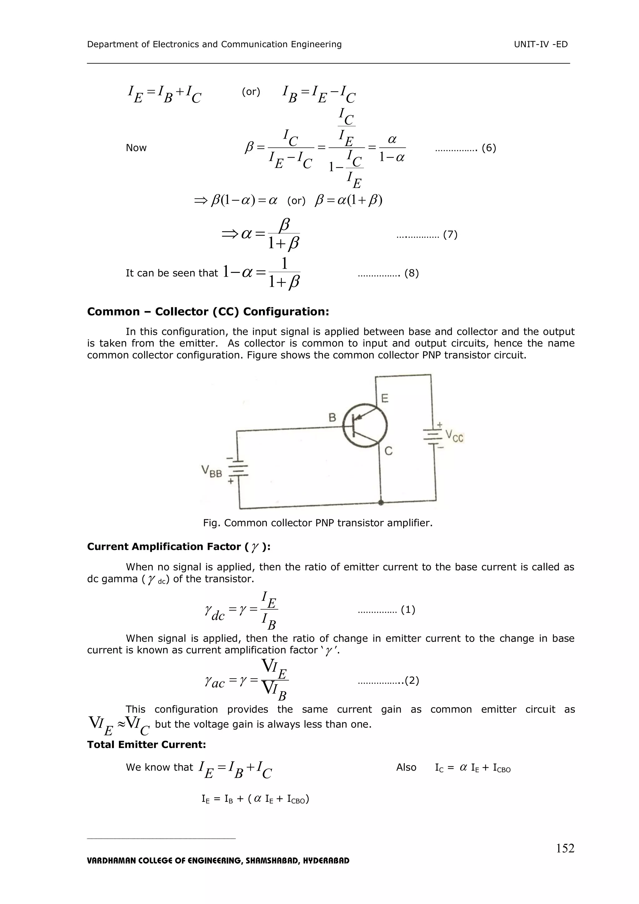
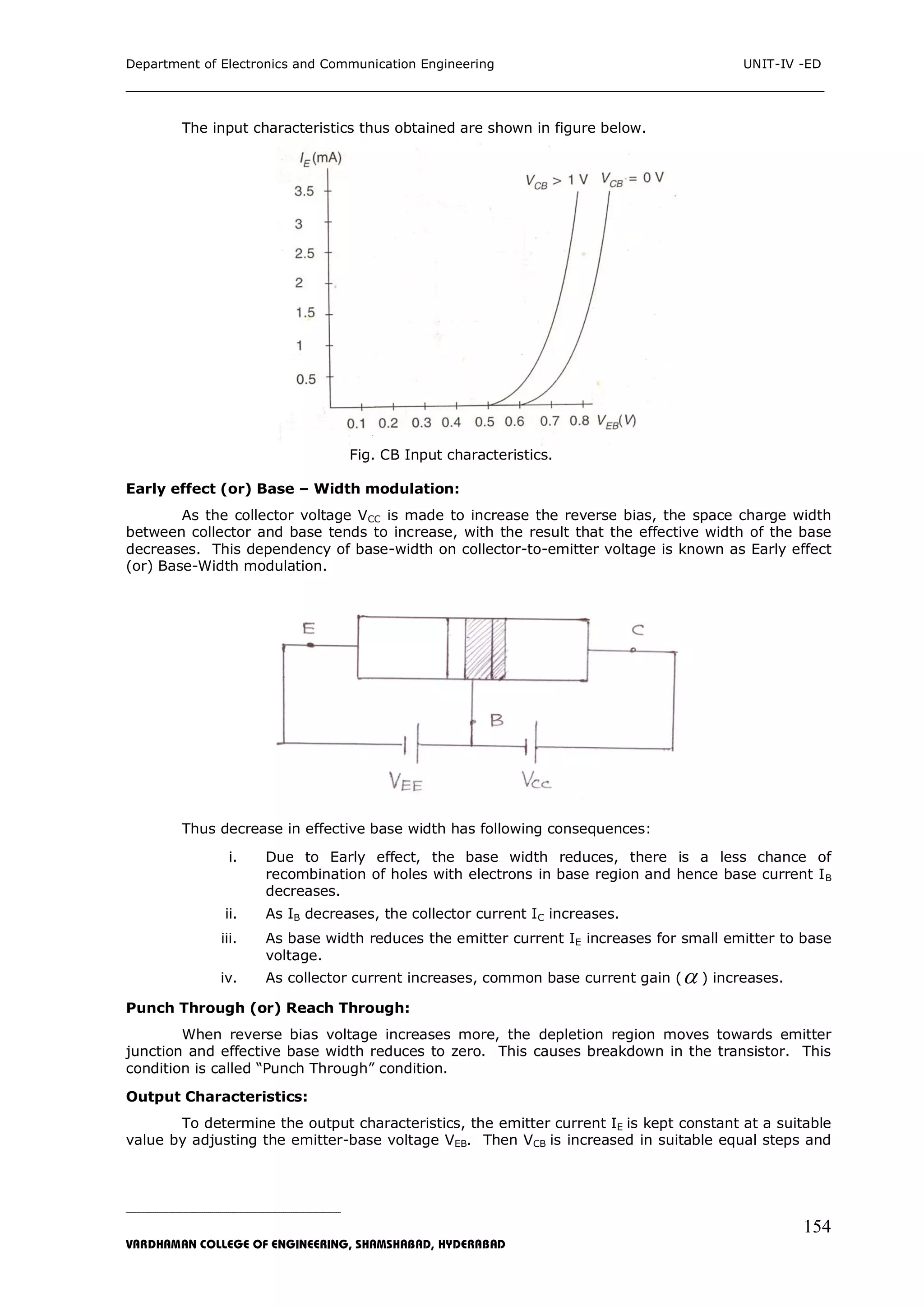
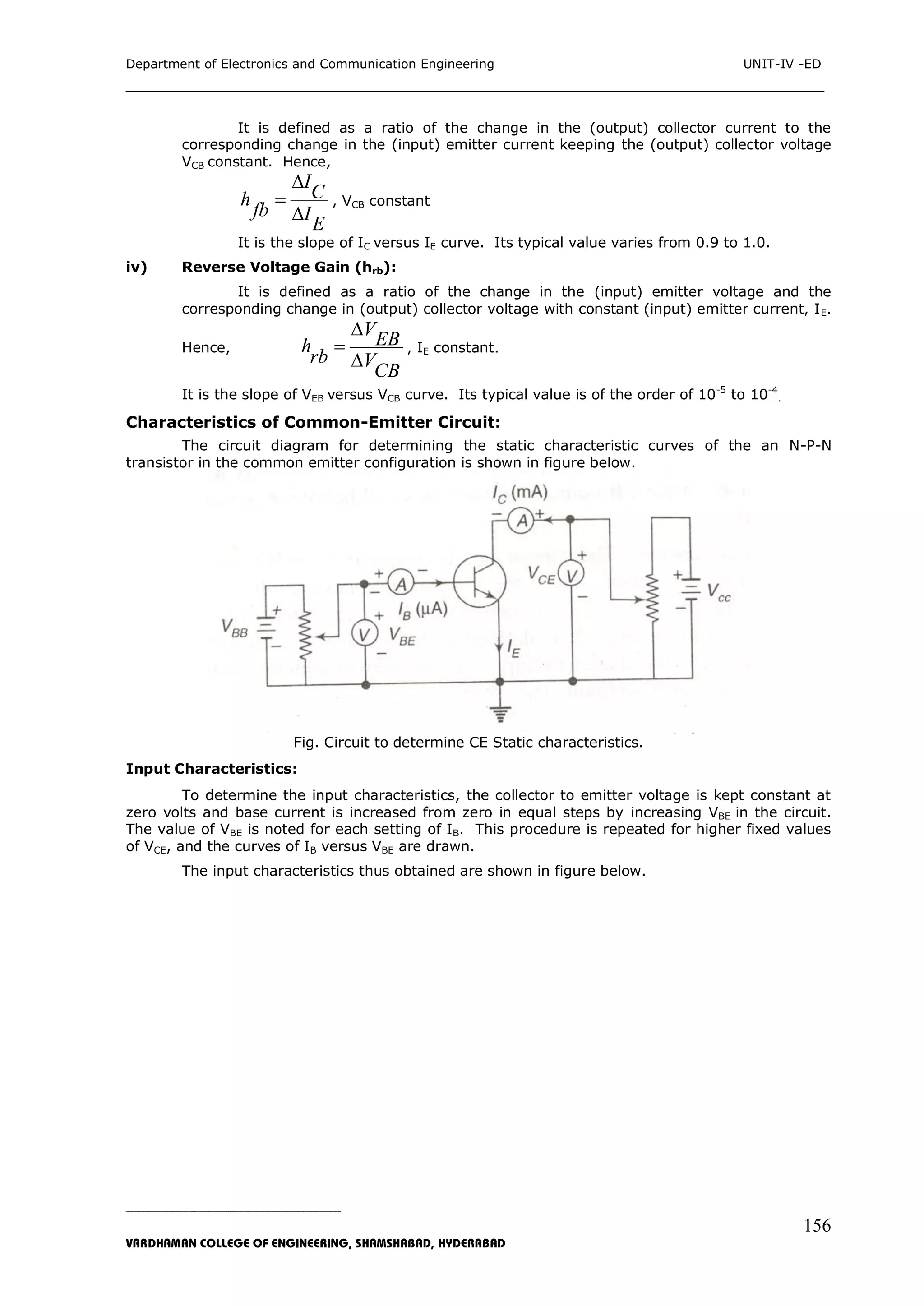
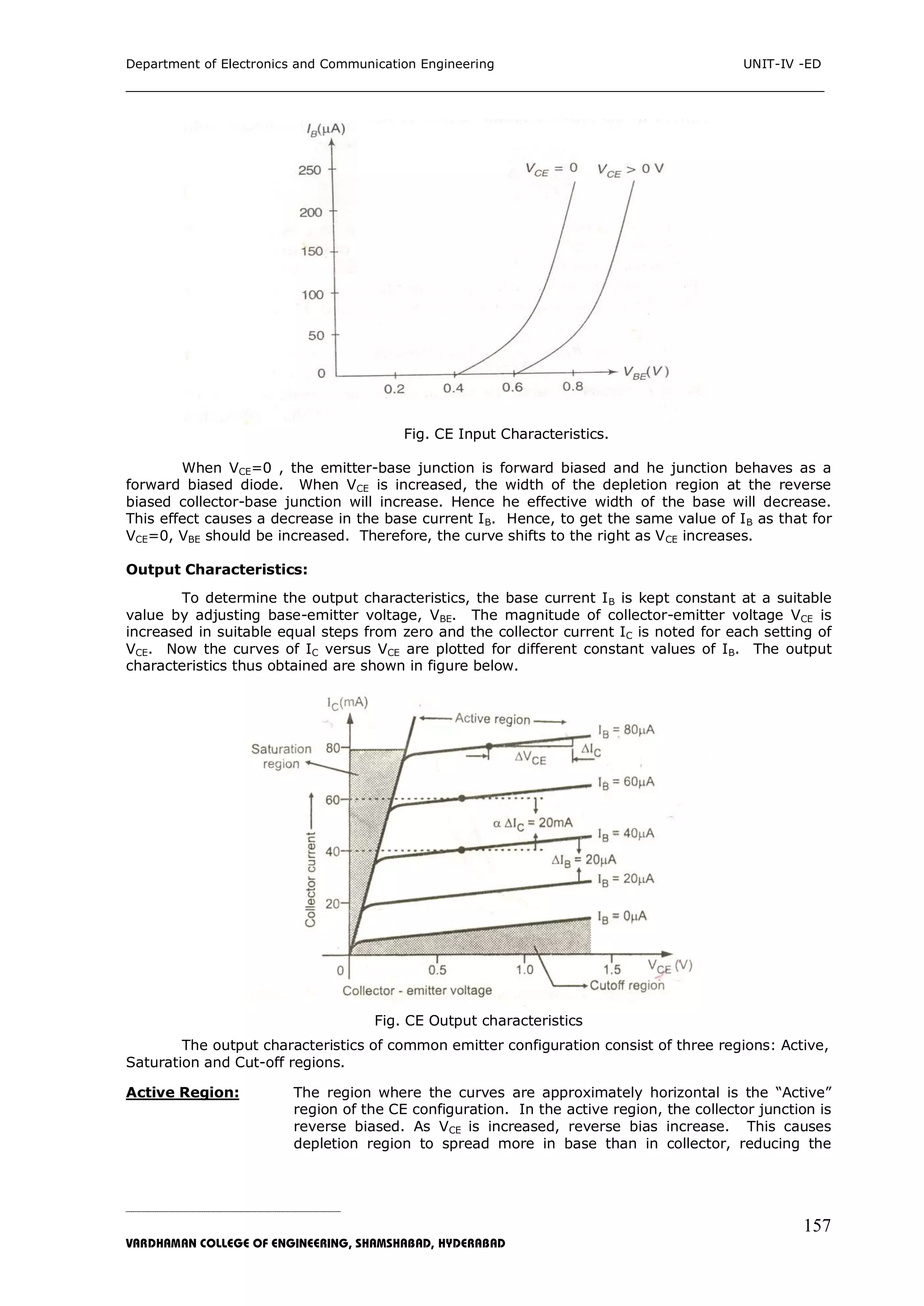
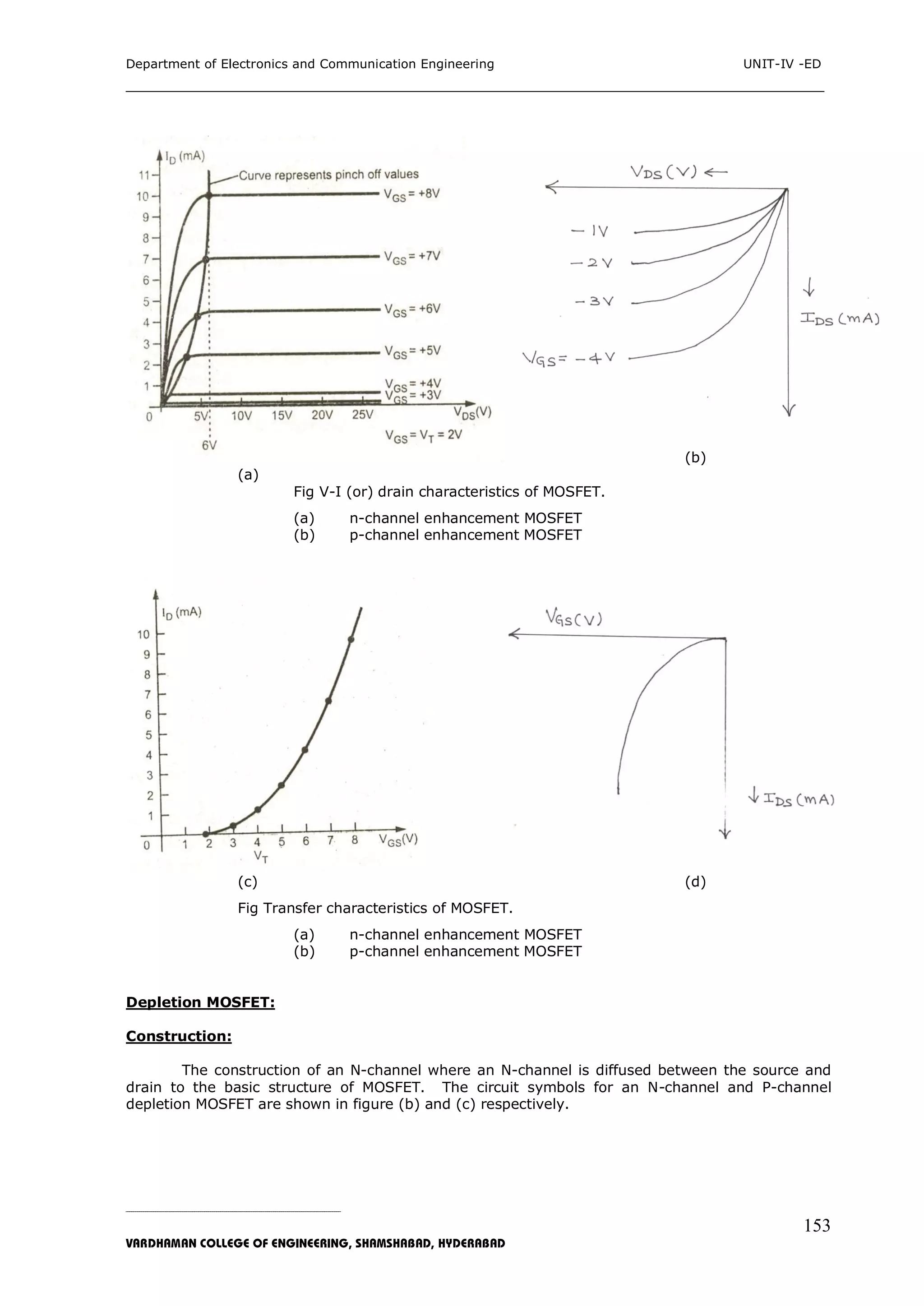
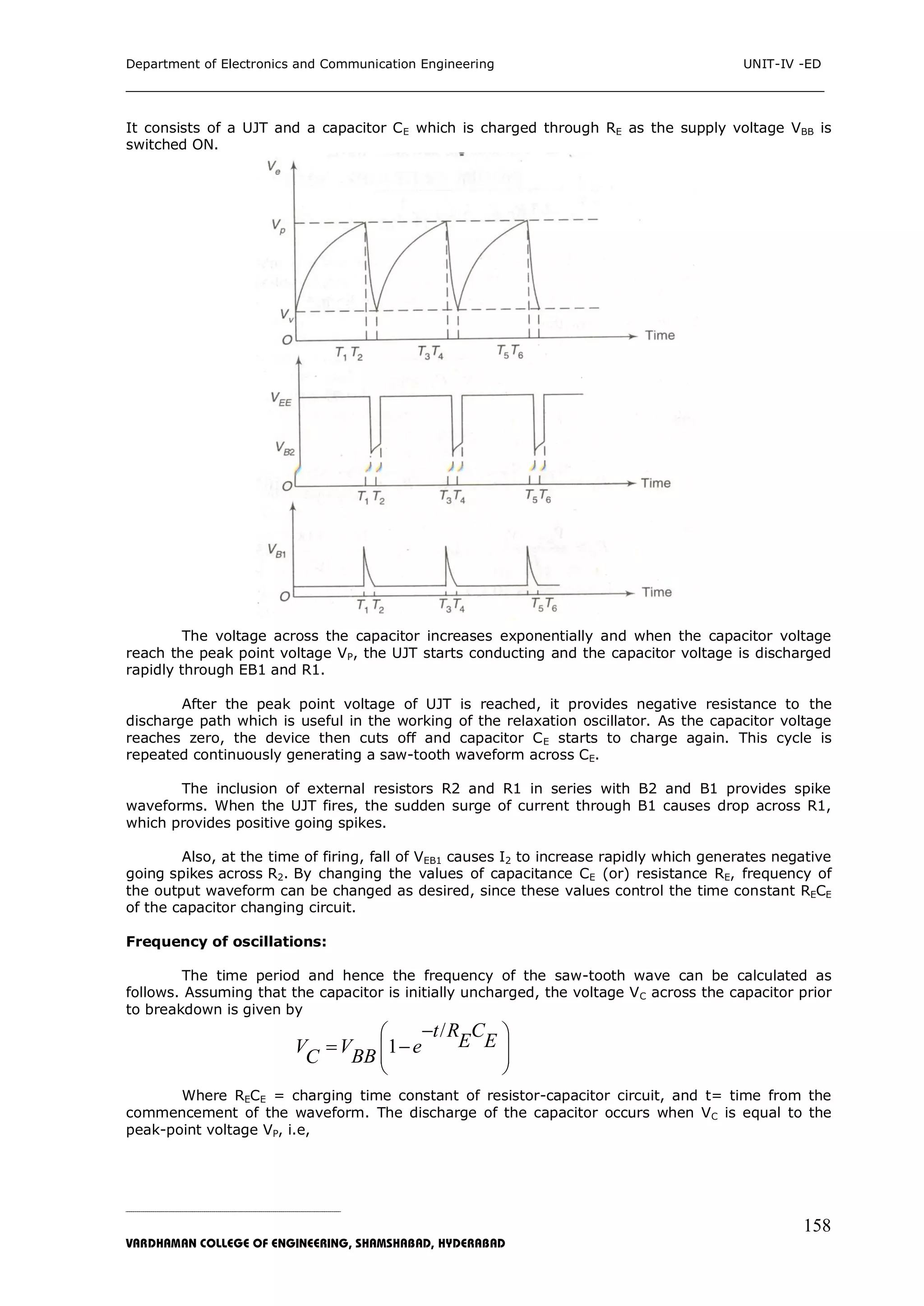
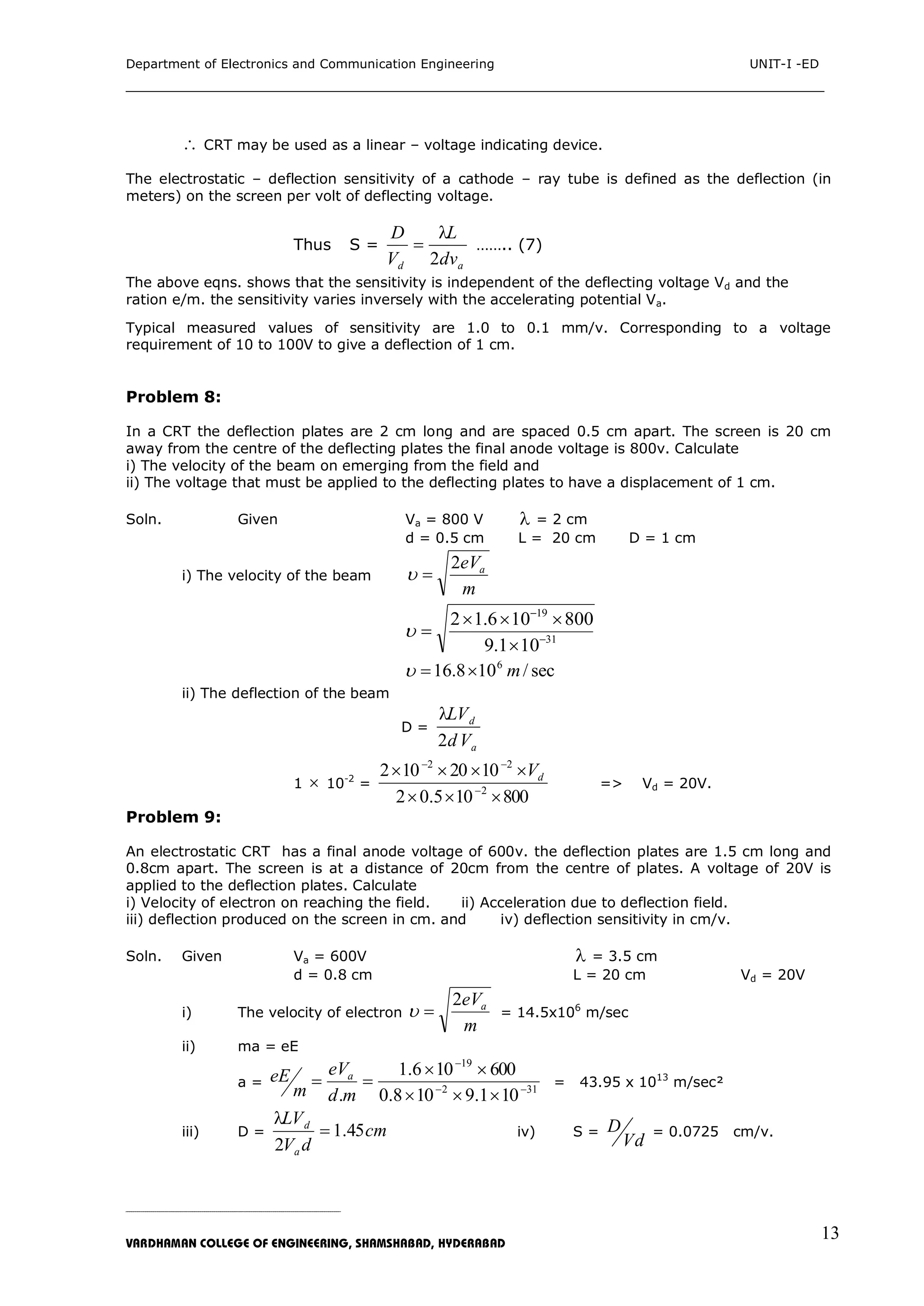
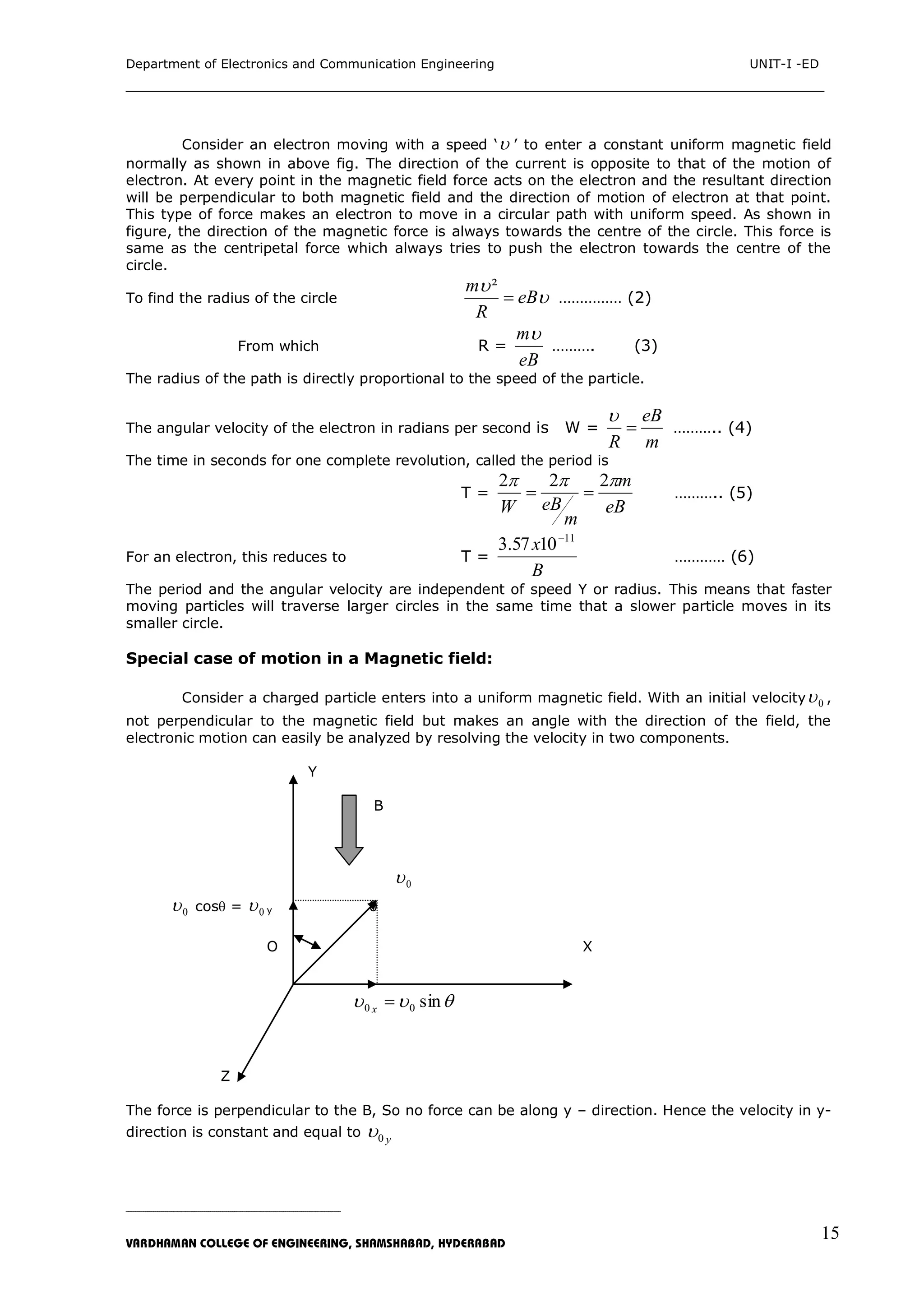
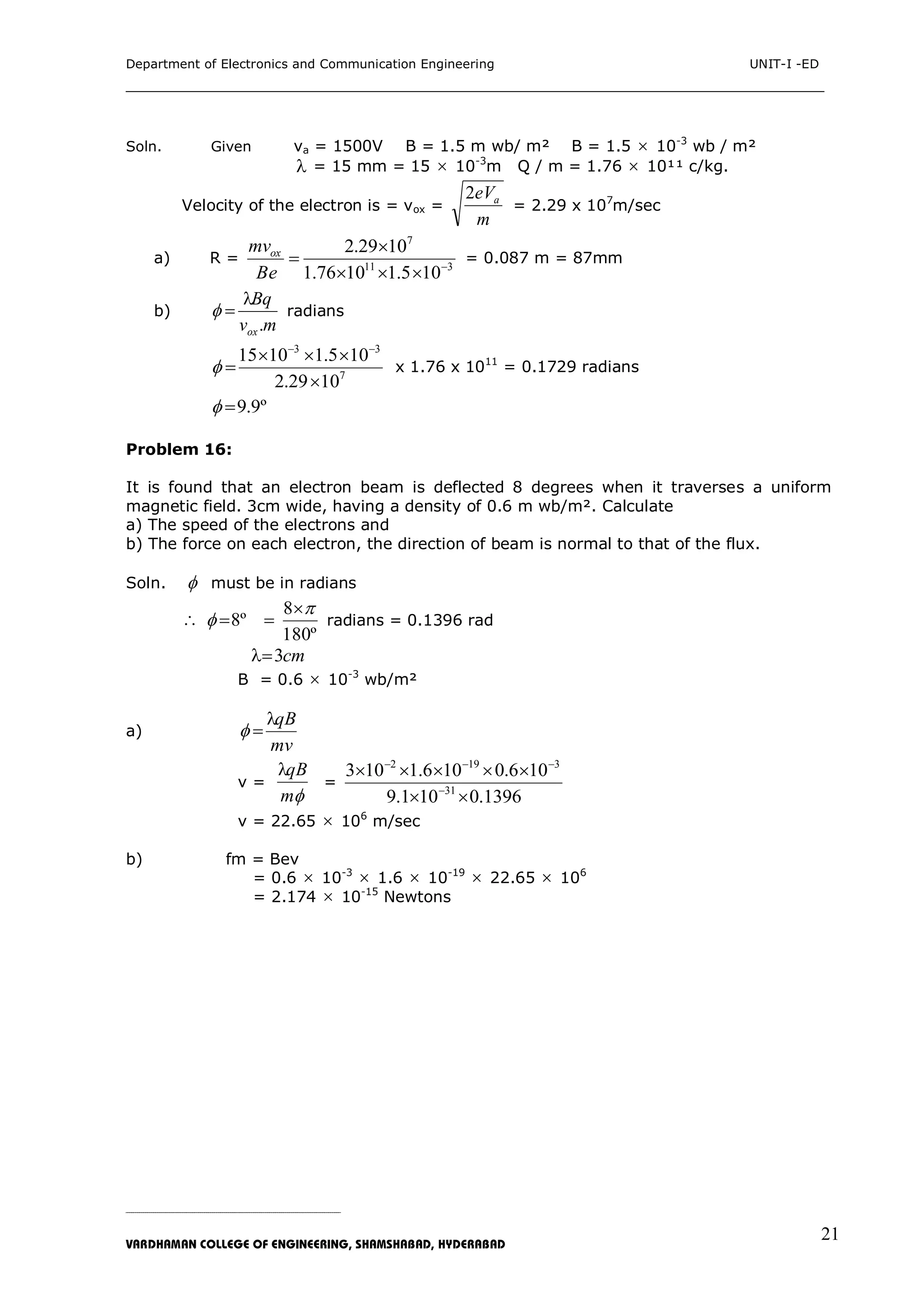
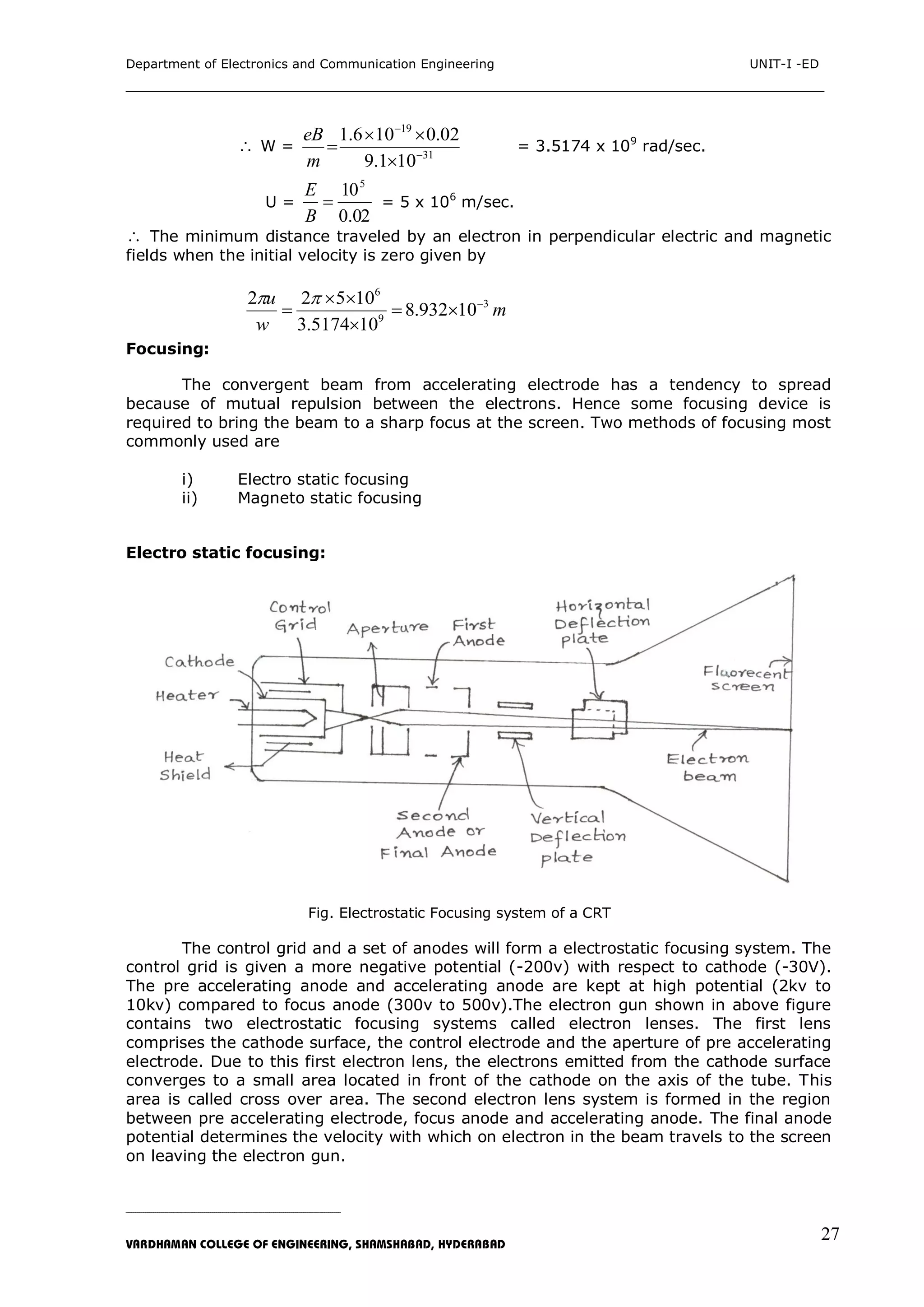
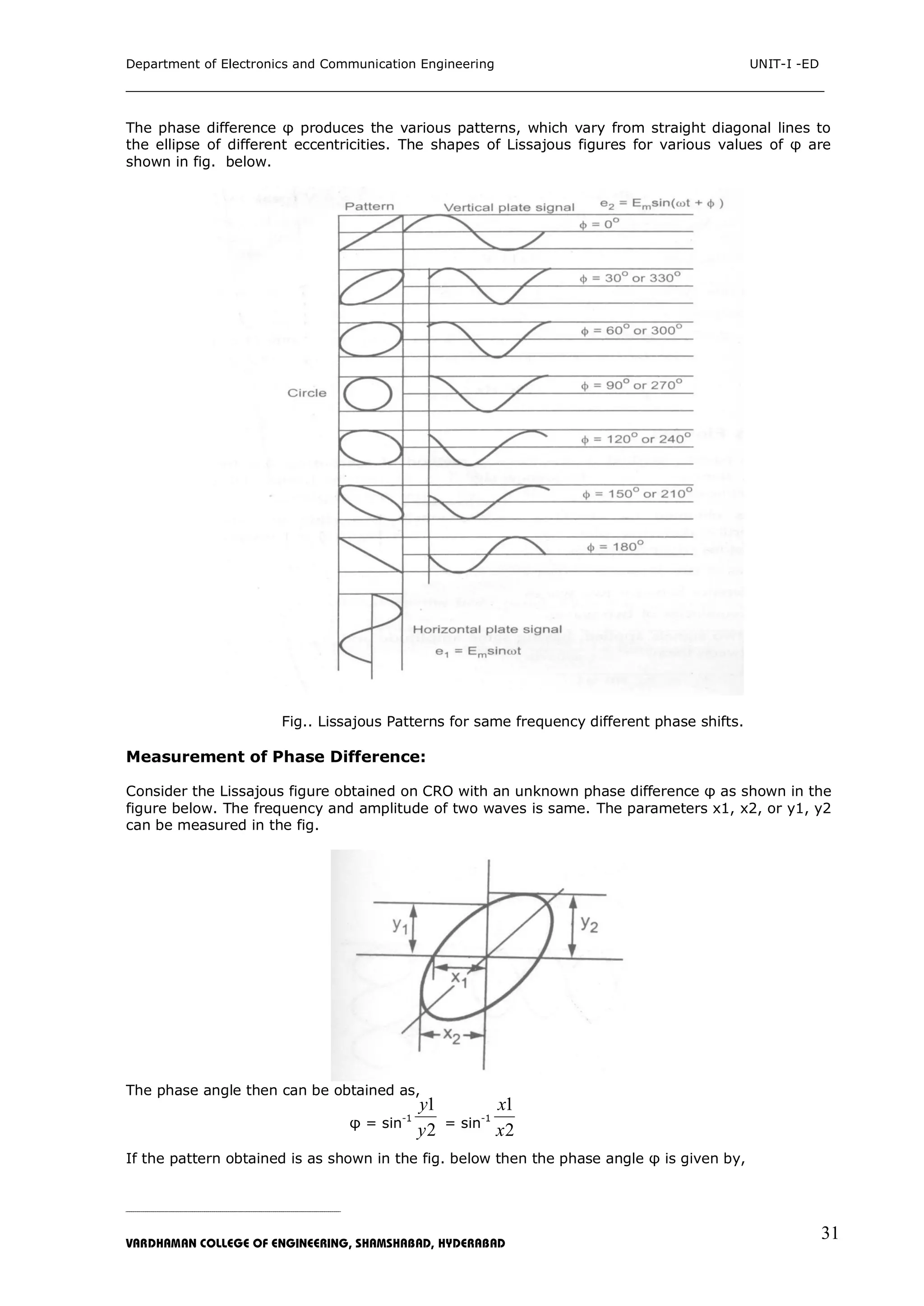
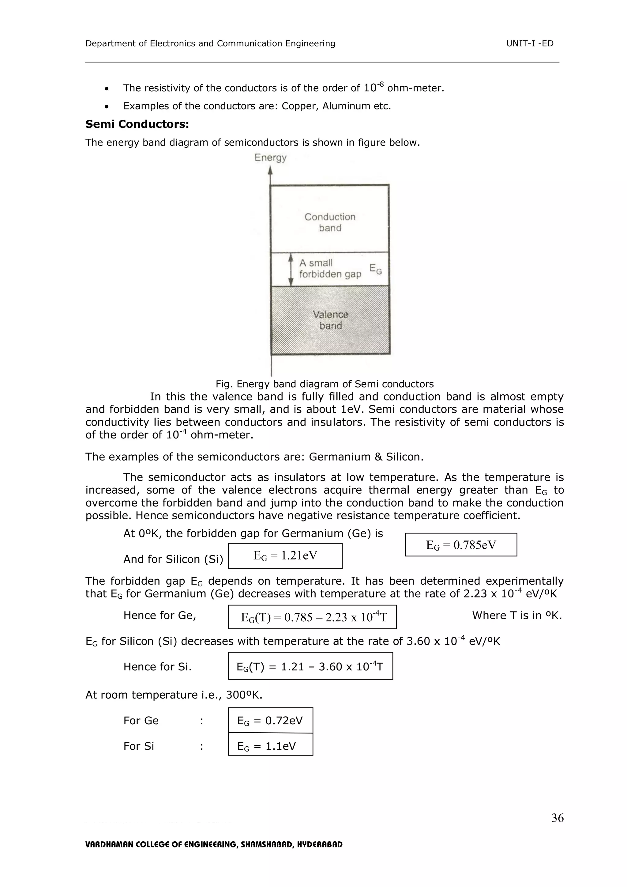
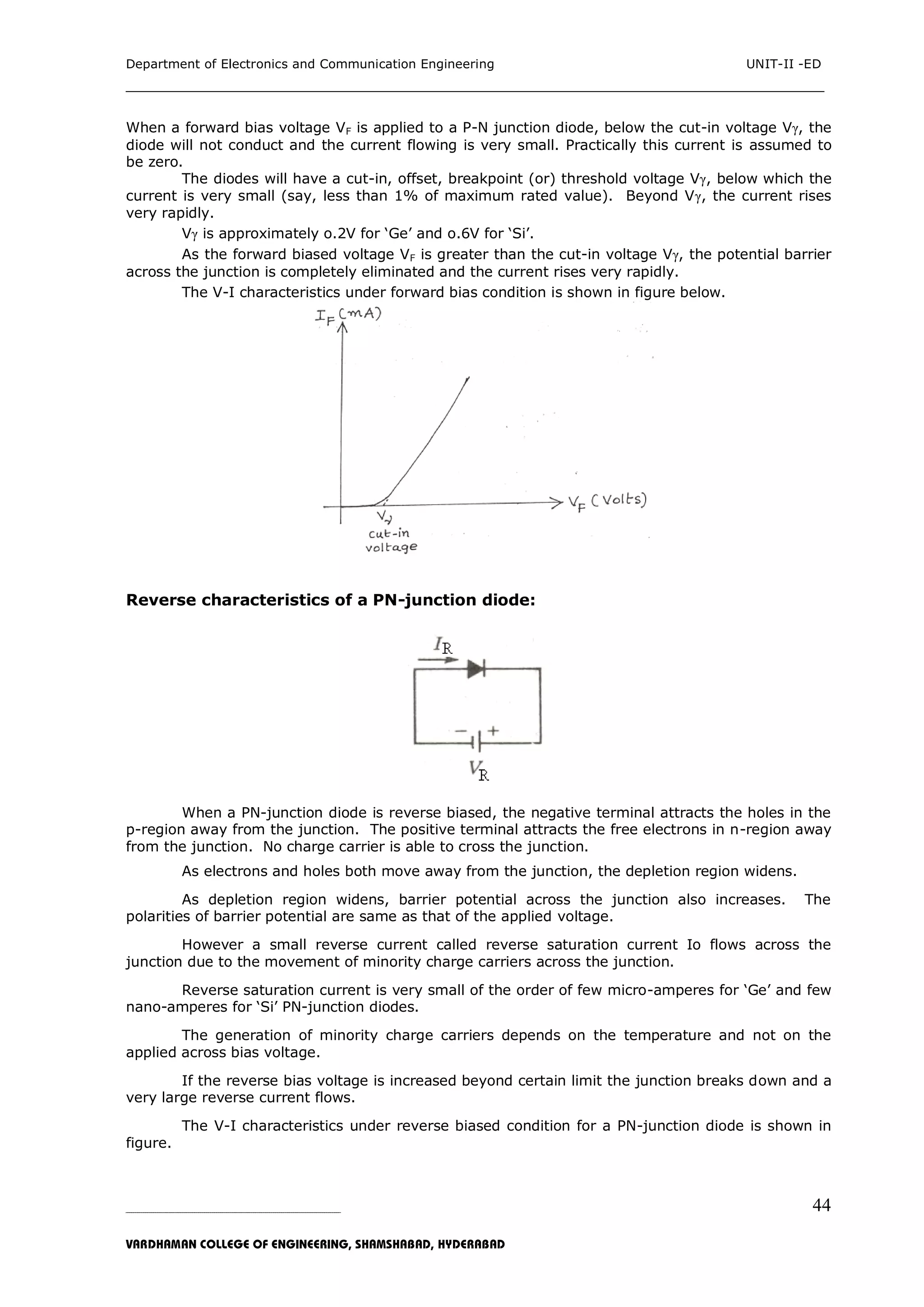
The document provides information about electron dynamics and cathode ray oscilloscopes (CROs). It includes:
1) A syllabus covering topics like motion of charged particles in electric and magnetic fields, principles of CRTs, deflection sensitivity, and motion of electrons in parallel and perpendicular electric and magnetic fields.
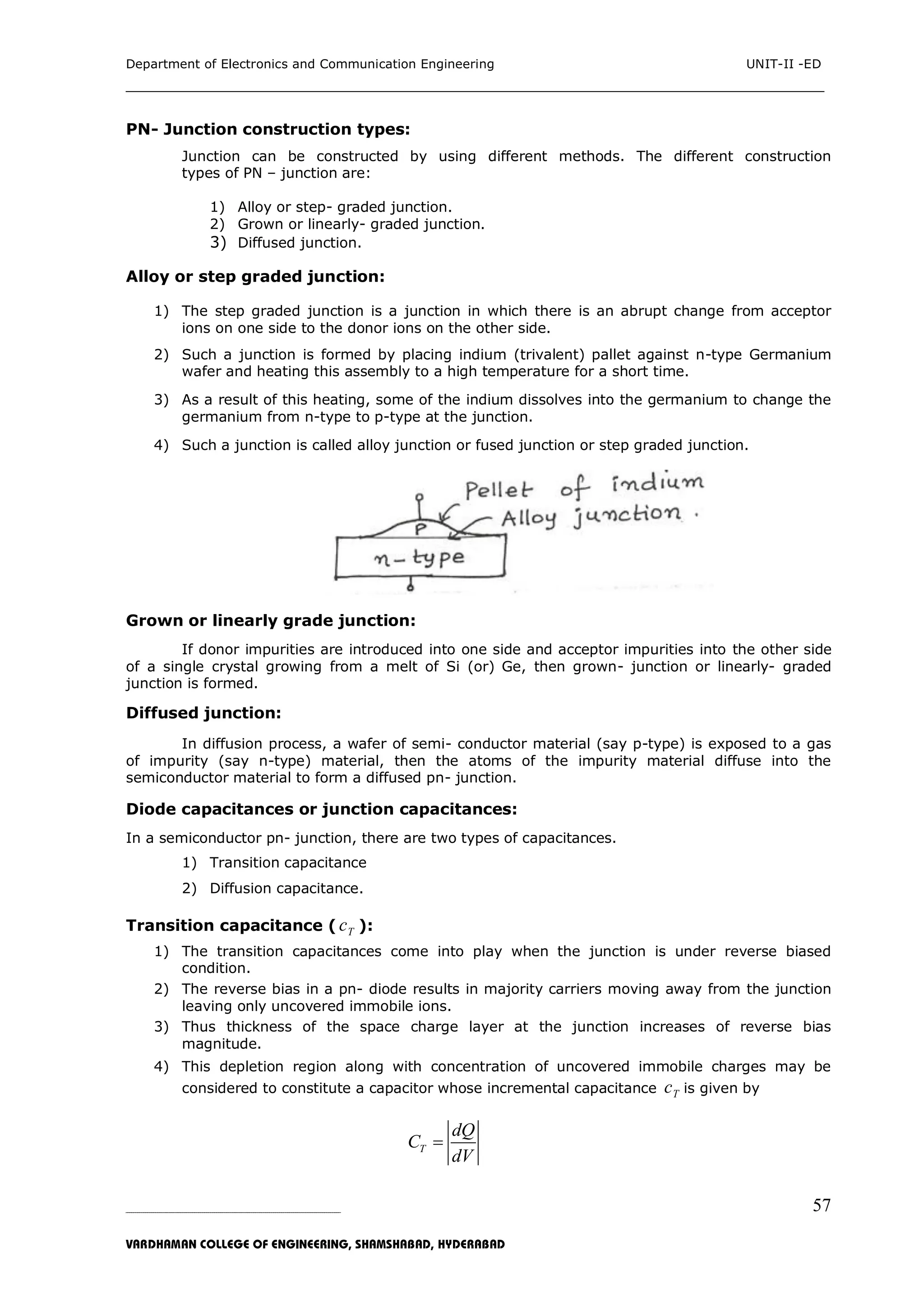
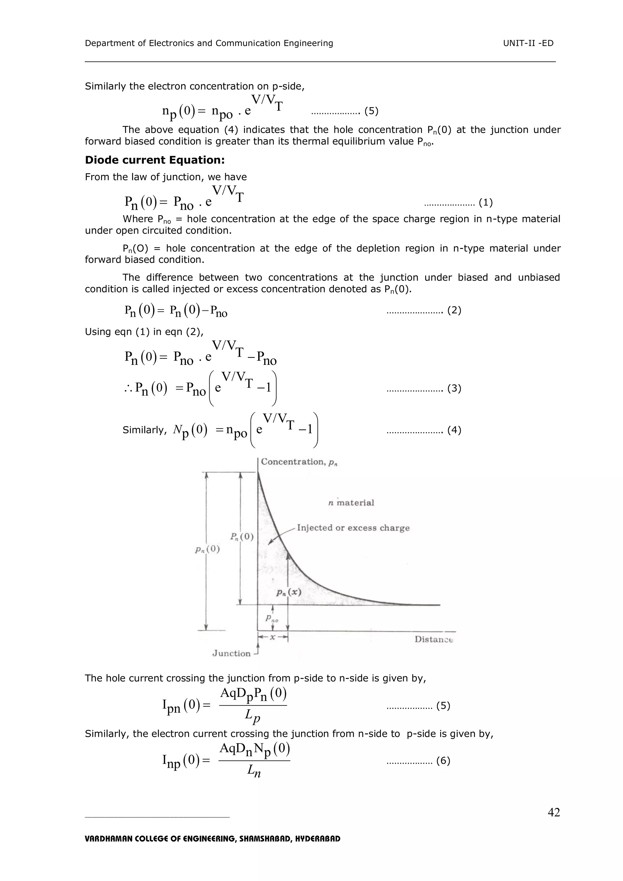
2) A lecture plan outlining topics to be covered in 15 periods, including introduction to Coulomb's law, CRO principles, deflection methods, and motion of electrons in various field configurations.
3) Concepts of electric and magnetic fields, forces on charged particles, electron velocity and path calculations, and examples solving for speed and position of an electron moving between capacitor plates.


![Department of Electronics and Communication Engineering UNIT-I -ED
___________________________________________________________________________
_____________________________________________________________________________________________________________
VARDHAMAN COLLEGE OF ENGINEERING, SHAMSHABAD, HYDERABAD
5
ax =
m
f
ax =
m
eE
m
f
dt
d x
f = eE
ax =
19
9
31
.602 10
2 10
9.1 10
eE
t
m
ax = (1.76 1011
) (2 109
t)
ax = 3.52 1020
t m/sec²
By integrating the above eqn. we obtain the speed.
t
xx dta
0
.
t
x dtt
0
20
1052.3
=3.52 x 10²⁰
.
1
02
²
t
= ²
2
1052.3 20
t
x = 1.76 x 10²⁰
t²
At t = 50n sec. x = 1.76 x 1020
x [50 x 10-9
]²
= 1.76 x 25 x 10² x
= 1.76 x 25 x 104
x = 4.40 x 10⁵
m/sec
b) Integration of x with respect to t, subject to the condition that x = 0 when t = 0 yields
x =
tt
x dttdt
0
20
0
²1076.1
x = 1.76 1020
1
03
³
t
= 5.87 1019
t³
At t = 50 n sec
x = 5.87 1019
[50 10-9
]³
x = 5.87 1019
53
10-24
= 7.32 10-3
m
x = 0.732 cm
c) To find the speed with which the electron strikes the positive plate, we first find the time„t‟ it
takes to reach that + plate.
t =
3
1
19
1087.5
x
T = sec1046.9
1087.5
05.0 8
3
1
19
Hence
x 1.76 1020
t²
= 1.76 1020
(9.46 10-8
]²
= 1.58 106
m/sec](https://image.slidesharecdn.com/edcnotes-180313093127/75/Edc-notes-5-2048.jpg)
![Department of Electronics and Communication Engineering UNIT-I -ED
___________________________________________________________________________
_____________________________________________________________________________________________________________
VARDHAMAN COLLEGE OF ENGINEERING, SHAMSHABAD, HYDERABAD
6
Problem from previous external Question paper
Problem 2
Two parallel plates of a capacitor are separated by 4 cms. An electron is at rest initially at the
bottom plate. Voltage is applied b/w the plates, which increases linearly from 0v to 8v in 0.1m sec.
If the Top plate is +ve, determine.
i) The speed of electron in 40n sec.
ii) The distance traversed by the electron in 40 n sec.
Solution: d = 4 cm = 4 10-2
m
V = t
t
43
10
8
101.0
8
E = tt
t
d
V 6
624
102
10
2
1010
2
v/m
i) a =
m
eE
m
F
dt
d
a = (1.76 1011
) 2 106
t
a = 3.52 1017
t m/sec²
t
dta
0
. = 3.52 1017
2
²t
= 1.76 1017
t²
= 1.376 1017
(40 10-9
)²= 1.76 16 101
10-1
= 1.76 x 160 m/sec.
ii)
t
dtx
0
=
t
t
0
217
1076.1 dt
x = 1.76 1017
3
³t
= 5.87 1016
t³
= 5.87 1016
[ 40 10-9
]3
m
Motion of electron with zero initial velocity in an electric field:
From Newton‟s second Law
F = max ……… (1)
F = -eEx ……… (2)
ax =
dt
d x
……… (3)
Substituting eqns. (2) or (3) in eqn. (1)
- eEx = m.
dt
d x
……….. (4)
By multiplying with „dx‟ both L.H.S & R.H.S
-eEx dx = m dx
dt
d x
.
-eExdx= m.d x. x x
dt
dx
Taking integration on both sides](https://image.slidesharecdn.com/edcnotes-180313093127/75/Edc-notes-6-2048.jpg)


![Department of Electronics and Communication Engineering UNIT-I -ED
___________________________________________________________________________
_____________________________________________________________________________________________________________
VARDHAMAN COLLEGE OF ENGINEERING, SHAMSHABAD, HYDERABAD
40
Where A0 = constant, independent of temperature.
T = Absolute temperature expressed in ºK.
EG0 = Forbidden energy gap at 0ºK.
K = Boltzman‟s constant expressed in eV/ºK
= 8.620 x 10⁻⁵
eV/ºK.
The intrinsic conductivity of Ge increases by approximately 5 percent per ºC and 7 percent per ºC
rise in temperature for silicon.
Properties of Germanium & Silicon
Property Ge Si
1. Atomic number 32 14
2. Atomic weight 72.6 28.1
3. Atoms / cm³ 4.4 x 10²² 5.0 x 10²²
4. EGO, eV at 0ºK 0.785 1.21
5. EG, eV at 300ºK 0.72 1.1
6. ni at 300ºK/ cm³ 2.5 x 10¹³
1.5 x 10¹⁰
7. µn, cm²/v-sec 3,800 1,300
8. µp, cm² / v-sec 1,800 500
9. Intrinsic resistivity at 300ºk ( -cm) 45 230,000
Problem: 2 Find the resistivity of an intrinsic silicon at 300ºk if intrinsic concentration of silicon at
300ºk is 1.5 1010
per cm³ while µn = 1300 cm²/v-sec and µp = 500 cm² / v-sec. Assume e = 1.6
x 10-19
C.
Soln. The given values are, ni = 1.5 x 10¹⁰
/ cm³
ni =
10
6
1.5x10
10
/m³
= 1.5 x 10¹⁶ / m³
And µn = 1300 x 10-4
m² / v-sec
µp = 500 x 10-4
m² / v-sec
Now i = ni (µn + µp) e
= 1.5 x 10¹⁶
[1300 + 500] x 10-4
x 1.6 x 10-19
= 0.000432 ( - m)-1
p =
i
1
=
000432.0
1
= 2314.8148 -m
Problem 3: Estimate the value of resistivity of intrinsic Germanium at 300ºk given:
Intrinsic concentration = 2.5 x 10¹³
cm³
Electron mobility = 3800 cm²/v-s
Hole mobility = 1800 cm² / v-s
Electron charge = 1.6 x 10⁻¹⁹
C.
Soln. Given values are Ni = 2.5 x 10¹³
/ cm³
ni =
13
6
2.5x10
10
= 2.5 x 10¹⁹/m³
µn = 3800 cm²/v-s = 3800 x 10-4
m²/v-s
µp = 1800 cm²/v-s = 1800 x 10-4
m²/v-s
i (µn + µp) nie
= (3800 + 1800) x 1.8 x 10-19
x 10-4
x 2.5 x 1019
= 2.24 ( -m)-1
i=
24.2
11
i
= 0.4464 -cm](https://image.slidesharecdn.com/edcnotes-180313093127/75/Edc-notes-40-2048.jpg)


![Department of Electronics and Communication Engineering UNIT-I -ED
___________________________________________________________________________
_____________________________________________________________________________________________________________
VARDHAMAN COLLEGE OF ENGINEERING, SHAMSHABAD, HYDERABAD
43
This expression is the concentration of electrons in conduction band.
The concentration of holes in the valence band is P =
VE
dEEfEN ………………….. (8)
When the maximum energy in the valence band is EV, the density of states is given by
N(E) = 2
1
EEV …………………… (9)
The Fermi function of a hole is [1 – f(E)] and is given by 1 – f(E) = 1 - KTEE F
e /
1
1
………… (10)
For E EV, E – EF << KT eqn. (10) reduces to 1 – f(E) =
KTEE F
e /
…………….. (11)
Substituting eqns. (9) & (11) in eqn. (8) we get P = dEEfEN
VE
1
P =
VE
KT
V eEE /E-E2
1
F
dE
=
dEe
KT
EE
KT KTEEEE
E
V VFV
V
/
2
1
2
1
.
=
dEeKTe
KT
EE
KT KTEEEE
E
V VFV
V
/
2
1
2
1
./.
Let dxKTdExKTEEx
KT
EE
V
V
When E = - x = E = EV x = 0
dxKTexeKTp xKTEE FV
0
2
1
/2
1
..
=
0
2
1
/2
3
. dxexeKT xKTEE FV
=
KTEE FV
eKT /2
3
KT
V eNP /E-E FV
………………………….. (12)
Where
2
3
KTNV
Therefore eqn. (12) is the expression for the concentration of holes in valence band.
Note: NC : Effective density of states in conduction band.
NV : Effective density of states in valence band
Fig. Band structure of Intrinsic semiconductor Fig. Fermi-Dirac prob. function f(E).](https://image.slidesharecdn.com/edcnotes-180313093127/75/Edc-notes-43-2048.jpg)


![Department of Electronics and Communication Engineering UNIT-II -ED
___________________________________________________________________________
_____________________________________________________________________________________________________________
VARDHAMAN COLLEGE OF ENGINEERING, SHAMSHABAD, HYDERABAD
56
For forward resistance use V =0.2V
32 x 26 x 10
r
f 0.25
36 2 x 26 x 102 x 10 x e
= 212.337Ω
For reverse resistance use V = 0.2V
32 x 26 x 10
rr 0.25
36 2 x 26 x 102 x 10 x e
= 3.1836MΩ
7) Find the value of dc resistance and ac resistance of a germanium junction diode at 25ºc
with IO =25µA and at an applied voltage of 0.2v across the diode.
Solution:
The dc resistance is the ratio of diode voltage and current at a point on V – I
characteristics.
Given : Vf =0.2V, IO =25µA, η =1 for Ge diode
V/ VTI I e 1o
Where VT =25+273/11,600 =0.025V
I = 25 x 10-6
[e0.2/(1 x 0.025)
- 1]
= 0.06013A
Rf = dc resistance = Vf/I = 0.2/0.06013 =3.3259Ω
and Rf =ac resistance = VT/ IO (eV/ηV
T)
= 0.025/25x10-6
x e(0.2/0.025 )
= 0.427Ω.
8) The voltage across a silicon diode at room temperature of 300ºk is 0.7v when 2ma current
flows through it. If the voltage increases to 0.75v, calculate the diode current assuming VT
= 26mv.
Solution:
V = 0.7V, η =2 for Si , VT = 26mV at 300ºK, I = 2mA
Now
V/ VTI I e 1o
2 x 10-3
= IO (e0.7/(2x26x10-3)
- 1 )
Io =2.8494 x 10⁻⁹
A
New voltage V = 0.75V,
V/ VTI I e 1o
= 2.8497 x 10⁻⁹
[e0.75/(2x26x10-3)
] = 5.2313mA.](https://image.slidesharecdn.com/edcnotes-180313093127/75/Edc-notes-79-2048.jpg)