Download to read offline
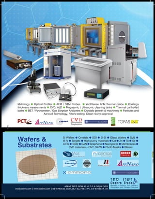
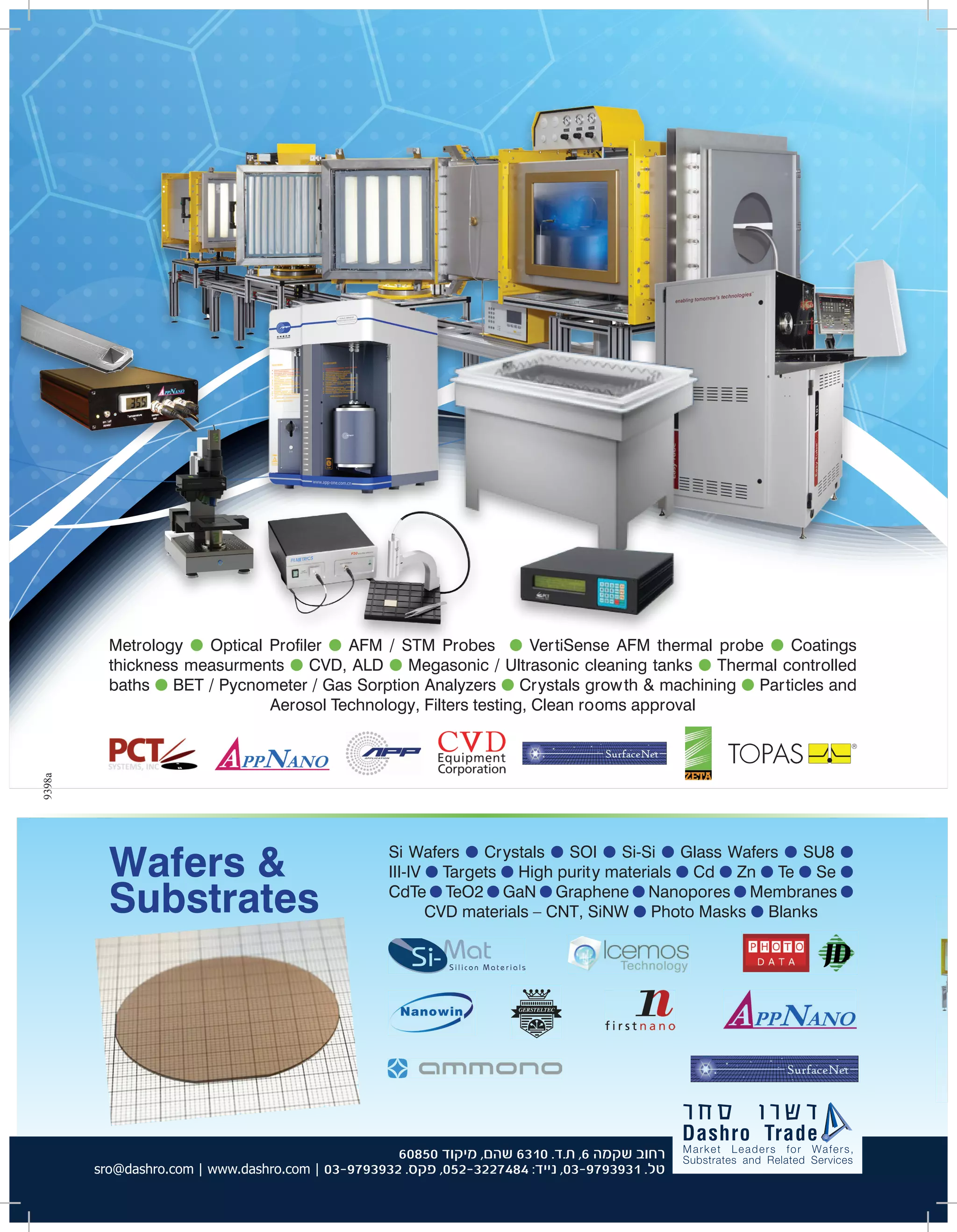

This document lists materials and equipment for semiconductor fabrication and metrology. It includes silicon wafers, crystals, SOI wafers, glass wafers, SU8, III-V compounds, targets, high purity elements, CdTe, TeO2, GaN, graphene, nanopores, membranes, CVD materials like CNTs and SiNWs, photo masks, and blanks. It also lists metrology equipment such as an optical profiler, AFM/STM probes, a VertiSense AFM thermal probe, thickness measurement tools, CVD and ALD systems, cleaning tanks, thermal baths, BET/pycnometer/gas sorption analyzers, crystal growth and machining equipment, and particle


