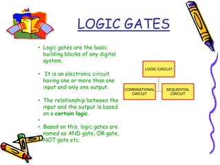
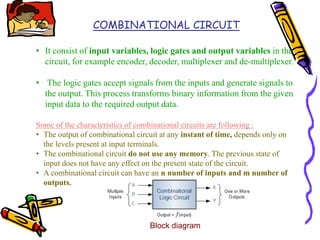
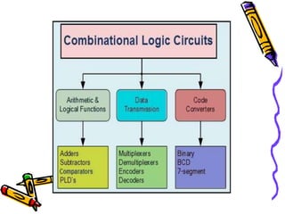
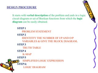
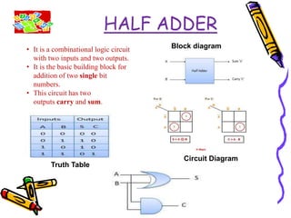
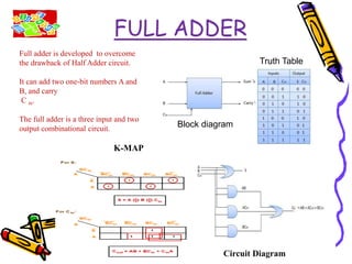
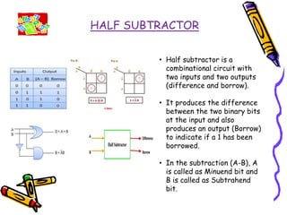
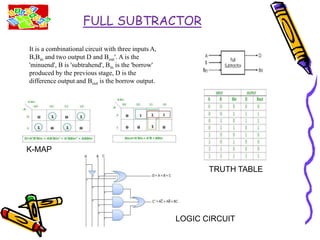
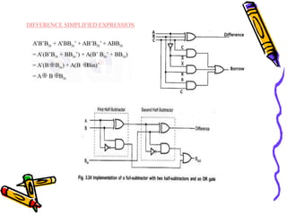
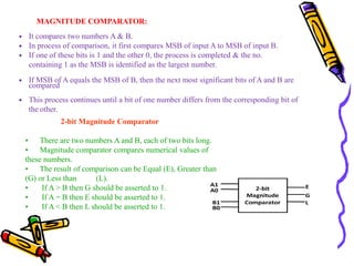
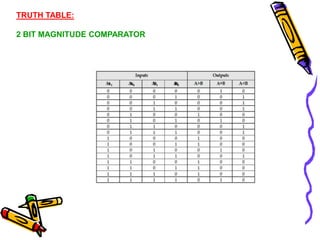
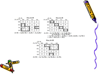
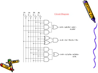
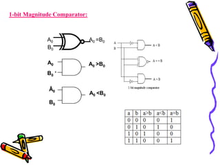
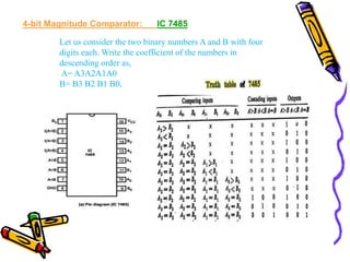
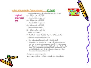
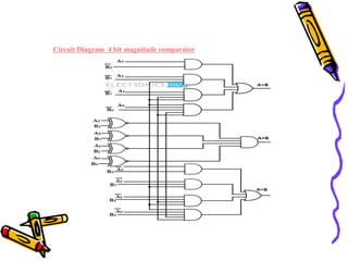
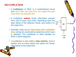
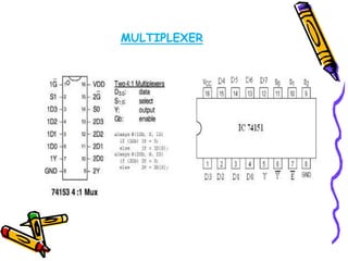
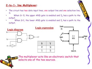
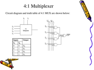
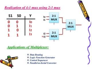
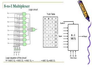
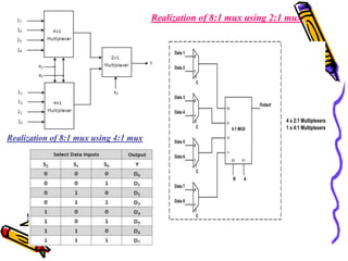
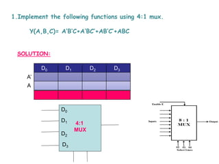
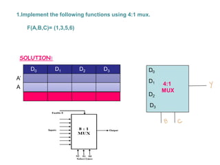
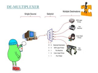
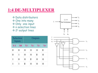
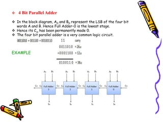
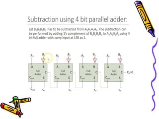
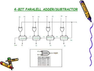
DIGITAL ELECTRONICS
Welcome, students!
By
Ms. P.Sivalakshmi AP/ECE
UNIT 2
COMBINATIONAL CIRCUIT DESIGN
 HALF & FULL ADDER
 HALF & FULL SUBTRACTOR
 BINARY PARALLEL ADDER
 CARRY LOOKAHEAD ADDER
 BCD ADDER
 MULTIPLEXER
 DEMULTIPLEXER
 MAGNITUDE COMPARATOR
 DECODER, ENCODER
 PRIORITY ENCODER
LOGIC GATES
LOGIC CIRCUIT
COMBINATIONAL
CIRCUIT
SEQUENTIAL
CIRCUIT
• Logic gates are the basic
building blocks of any digital
system.
• It is an electronic circuit
having one or more than one
input and only one output.
• The relationship between the
input and the output is based
on a certain logic.
•
• Based on this, logic gates are
named as AND gate, OR gate,
NOT gate etc.
COMBINATIONAL CIRCUIT
• It consist of input variables, logic gates and output variables in the
circuit, for example encoder, decoder, multiplexer and de-multiplexer.
• The logic gates accept signals from the inputs and generate signals to
the output. This process transforms binary information from the given
input data to the required output data.
Some of the characteristics of combinational circuits are following :
• The output of combinational circuit at any instant of time, depends only on
the levels present at input terminals.
• The combinational circuit do not use any memory. The previous state of
input does not have any effect on the present state of the circuit.
• A combinational circuit can have an n number of inputs and m number of
outputs.
Block diagram
DESIGN PROCEDURE
It starts with verbal description of the problem and ends in a logic
circuit diagram or set of Boolean functions from which the logic
diagram can be easily obtained.
STEP 1
PROBLEM STATEMENT
STEP 2
IDENTITFY THE NUMBER OF I/P AND O/P
VARIABLES & GIVE THE BLOCK DIAGRAM.
STEP 3
TRUTH TABLE
STEP 4
K-MAP
STEP 5
SIMPLIFIED LOGIC EXPRESSION
STEP 6:
LOGIC DIAGRAM
HALF ADDER
• It is a combinational logic circuit
with two inputs and two outputs.
• It is the basic building block for
addition of two single bit
numbers.
• This circuit has two
outputs carry and sum.
Block diagram
Truth Table
Circuit Diagram
FULL ADDER
Full adder is developed to overcome
the drawback of Half Adder circuit.
It can add two one-bit numbers A and
B, and carry
C in.
The full adder is a three input and two
output combinational circuit.
Block diagram
Truth Table
K-MAP
Circuit Diagram
IMPLEMENTATION OF FULLADDER USING TWO HALF ADDER
HALF SUBTRACTOR
• Half subtractor is a
combinational circuit with
two inputs and two outputs
(difference and borrow).
• It produces the difference
between the two binary bits
at the input and also
produces an output (Borrow)
to indicate if a 1 has been
borrowed.
• In the subtraction (A-B), A
is called as Minuend bit and
B is called as Subtrahend
bit.
FULL SUBTRACTOR
LOGIC CIRCUIT
TRUTH TABLE
K-MAP
It is a combinational circuit with three inputs A,
B,Bin and two output D and Bout'. A is the
'minuend', B is 'subtrahend', Bin is the 'borrow'
produced by the previous stage, D is the
difference output and Bout is the borrow output.
DIFFERENCE SIMPLIFIED EXPRESSION
MAGNITUDE COMPARATOR:
 It compares two numbers A & B.
 In process of comparison, it first compares MSB of input A to MSB of input B.
 If one of these bits is 1 and the other 0, the process is completed & the no.
containing 1 as the MSB is identified as the largest number.
 If MSB of A equals the MSB of B, then the next most significant bits of A and B are
compared
 This process continues until a bit of one number differs from the corresponding bit of
the other.
2-bit Magnitude Comparator
• There are two numbers A and B, each of two bits long.
• Magnitude comparator compares numerical values of
these numbers.
• The result of comparison can be Equal (E), Greater than
(G) or Less than (L).
• If A > B then G should be asserted to 1.
• If A = B then E should be asserted to 1.
• If A < B then L should be asserted to 1.
TRUTH TABLE:
2 BIT MAGNITUDE COMPARATOR
A1 A0 B1 B0
Circuit Diagram
A0
B0
A0 =B0
A0 A0 >B0
B0 ‘
A0 <B0
B0
Ā0
1-bit Magnitude Comparator:
4-bit Magnitude Comparator: IC 7485
Let us consider the two binary numbers A and B with four
digits each. Write the coefficient of the numbers in
descending order as,
A= A3A2A1A0
B= B3 B2 B1 B0,
4-bit Magnitude Comparator: IC 7485
Logical
expressi
ons
Circuit Diagram 4 bit magnitude comparator
• A multiplexer or MUX, is a combinational circuit
with more than one input line, one output line and
more than one selection line.
• A multiplexer selects binary information present
from one of many input lines, depending upon the
logic status of the selection inputs, and routes it to
the output line.
• Normally, there are 2n input lines and n selection
lines whose bit combinations determine which input
is selected. The multiplexer is often labelled as
MUX in block diagrams.
• A multiplexer is also called a data selector, since it
selects one of many inputs and steers the binary
information to the output line.
MULTIPLEXER
MULTIPLEXER
MULTIPLEXER
2-to-1- line Multiplexer:
• The circuit has two data input lines, one output line and one selection line,
S.
• When S= 0, the upper AND gate is enabled and I0 has a path to the
output.
• When S=1, the lower AND gate is enabled and I1 has a path to the
output.
Logic diagram
The multiplexer acts like an electronic switch that
selects one of the two sources.
Logic expression
Realization of 4:1 mux using 2:1 mux
Applications of Multiplexer:
 Data Routing
 Logic Function Generator
 Control Sequencer
 Parallel-to-Serial Converter
Realization of 8:1 mux using 2:1 mux
Realization of 8:1 mux using 4:1 mux
1.Implement the following functions using 4:1 mux.
Y(A,B,C)= A’B’C+A’BC’+AB’C’+ABC
SOLUTION:
A’
A
D0 D1 D2 D3
D0
D1
D2
D3
4:1
MUX
1.Implement the following functions using 4:1 mux.
F(A,B,C)= (1,3,5,6)
SOLUTION:
A’
A
D0 D1 D2 D3
DE-MULTIPLEXER
1:4 DE-MULTIPLEXER
 Data distributors
 One into many
 Only one input
 n selection lines
 2n output lines
Selection
Inputs
Outputs
S 1 S0 Y3 Y2 Y1 Y0
0 0 0 0 0 I
0 1 0 0 I 0
1 0 0 I 0 0
1 1 I 0 0 0
 4 Bit Parallel Adder
 In the block diagram, A0 and B0 represent the LSB of the four bit
words A and B. Hence Full Adder-0 is the lowest stage.
 Hence its Cin has been permanently made 0.
 The four bit parallel adder is a very common logic circuit.
EXAMPLE
4-BIT PARALELL ADDER/SUBTRACTOR
Let’s Have a great Day!

Combinational circuit

  • 1.
  • 2.
    UNIT 2 COMBINATIONAL CIRCUITDESIGN  HALF & FULL ADDER  HALF & FULL SUBTRACTOR  BINARY PARALLEL ADDER  CARRY LOOKAHEAD ADDER  BCD ADDER  MULTIPLEXER  DEMULTIPLEXER  MAGNITUDE COMPARATOR  DECODER, ENCODER  PRIORITY ENCODER
  • 3.
    LOGIC GATES LOGIC CIRCUIT COMBINATIONAL CIRCUIT SEQUENTIAL CIRCUIT •Logic gates are the basic building blocks of any digital system. • It is an electronic circuit having one or more than one input and only one output. • The relationship between the input and the output is based on a certain logic. • • Based on this, logic gates are named as AND gate, OR gate, NOT gate etc.
  • 4.
    COMBINATIONAL CIRCUIT • Itconsist of input variables, logic gates and output variables in the circuit, for example encoder, decoder, multiplexer and de-multiplexer. • The logic gates accept signals from the inputs and generate signals to the output. This process transforms binary information from the given input data to the required output data. Some of the characteristics of combinational circuits are following : • The output of combinational circuit at any instant of time, depends only on the levels present at input terminals. • The combinational circuit do not use any memory. The previous state of input does not have any effect on the present state of the circuit. • A combinational circuit can have an n number of inputs and m number of outputs. Block diagram
  • 6.
    DESIGN PROCEDURE It startswith verbal description of the problem and ends in a logic circuit diagram or set of Boolean functions from which the logic diagram can be easily obtained. STEP 1 PROBLEM STATEMENT STEP 2 IDENTITFY THE NUMBER OF I/P AND O/P VARIABLES & GIVE THE BLOCK DIAGRAM. STEP 3 TRUTH TABLE STEP 4 K-MAP STEP 5 SIMPLIFIED LOGIC EXPRESSION STEP 6: LOGIC DIAGRAM
  • 7.
    HALF ADDER • Itis a combinational logic circuit with two inputs and two outputs. • It is the basic building block for addition of two single bit numbers. • This circuit has two outputs carry and sum. Block diagram Truth Table Circuit Diagram
  • 8.
    FULL ADDER Full adderis developed to overcome the drawback of Half Adder circuit. It can add two one-bit numbers A and B, and carry C in. The full adder is a three input and two output combinational circuit. Block diagram Truth Table K-MAP Circuit Diagram
  • 9.
    IMPLEMENTATION OF FULLADDERUSING TWO HALF ADDER
  • 10.
    HALF SUBTRACTOR • Halfsubtractor is a combinational circuit with two inputs and two outputs (difference and borrow). • It produces the difference between the two binary bits at the input and also produces an output (Borrow) to indicate if a 1 has been borrowed. • In the subtraction (A-B), A is called as Minuend bit and B is called as Subtrahend bit.
  • 11.
    FULL SUBTRACTOR LOGIC CIRCUIT TRUTHTABLE K-MAP It is a combinational circuit with three inputs A, B,Bin and two output D and Bout'. A is the 'minuend', B is 'subtrahend', Bin is the 'borrow' produced by the previous stage, D is the difference output and Bout is the borrow output.
  • 12.
  • 13.
    MAGNITUDE COMPARATOR:  Itcompares two numbers A & B.  In process of comparison, it first compares MSB of input A to MSB of input B.  If one of these bits is 1 and the other 0, the process is completed & the no. containing 1 as the MSB is identified as the largest number.  If MSB of A equals the MSB of B, then the next most significant bits of A and B are compared  This process continues until a bit of one number differs from the corresponding bit of the other. 2-bit Magnitude Comparator • There are two numbers A and B, each of two bits long. • Magnitude comparator compares numerical values of these numbers. • The result of comparison can be Equal (E), Greater than (G) or Less than (L). • If A > B then G should be asserted to 1. • If A = B then E should be asserted to 1. • If A < B then L should be asserted to 1.
  • 14.
    TRUTH TABLE: 2 BITMAGNITUDE COMPARATOR A1 A0 B1 B0
  • 16.
  • 17.
    A0 B0 A0 =B0 A0 A0>B0 B0 ‘ A0 <B0 B0 Ā0 1-bit Magnitude Comparator:
  • 18.
    4-bit Magnitude Comparator:IC 7485 Let us consider the two binary numbers A and B with four digits each. Write the coefficient of the numbers in descending order as, A= A3A2A1A0 B= B3 B2 B1 B0,
  • 19.
    4-bit Magnitude Comparator:IC 7485 Logical expressi ons
  • 20.
    Circuit Diagram 4bit magnitude comparator
  • 21.
    • A multiplexeror MUX, is a combinational circuit with more than one input line, one output line and more than one selection line. • A multiplexer selects binary information present from one of many input lines, depending upon the logic status of the selection inputs, and routes it to the output line. • Normally, there are 2n input lines and n selection lines whose bit combinations determine which input is selected. The multiplexer is often labelled as MUX in block diagrams. • A multiplexer is also called a data selector, since it selects one of many inputs and steers the binary information to the output line. MULTIPLEXER
  • 22.
  • 23.
  • 24.
    2-to-1- line Multiplexer: •The circuit has two data input lines, one output line and one selection line, S. • When S= 0, the upper AND gate is enabled and I0 has a path to the output. • When S=1, the lower AND gate is enabled and I1 has a path to the output. Logic diagram The multiplexer acts like an electronic switch that selects one of the two sources. Logic expression
  • 26.
    Realization of 4:1mux using 2:1 mux Applications of Multiplexer:  Data Routing  Logic Function Generator  Control Sequencer  Parallel-to-Serial Converter
  • 28.
    Realization of 8:1mux using 2:1 mux Realization of 8:1 mux using 4:1 mux
  • 29.
    1.Implement the followingfunctions using 4:1 mux. Y(A,B,C)= A’B’C+A’BC’+AB’C’+ABC SOLUTION: A’ A D0 D1 D2 D3 D0 D1 D2 D3 4:1 MUX
  • 30.
    1.Implement the followingfunctions using 4:1 mux. F(A,B,C)= (1,3,5,6) SOLUTION: A’ A D0 D1 D2 D3
  • 31.
  • 32.
    1:4 DE-MULTIPLEXER  Datadistributors  One into many  Only one input  n selection lines  2n output lines Selection Inputs Outputs S 1 S0 Y3 Y2 Y1 Y0 0 0 0 0 0 I 0 1 0 0 I 0 1 0 0 I 0 0 1 1 I 0 0 0
  • 33.
     4 BitParallel Adder  In the block diagram, A0 and B0 represent the LSB of the four bit words A and B. Hence Full Adder-0 is the lowest stage.  Hence its Cin has been permanently made 0.  The four bit parallel adder is a very common logic circuit. EXAMPLE
  • 35.
  • 36.
    Let’s Have agreat Day!