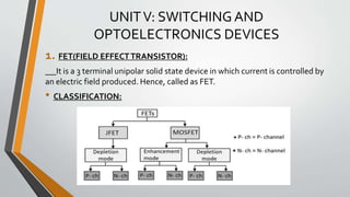
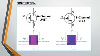
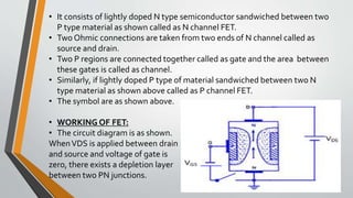
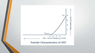
B.Sc I Sem I Electronics
- Prof. D.B.Bobade
Three terminal IC regulator
• It consists of three pins having 3 standard pin configuration i.e. Pin no. 1
indicates unregulated i/p voltage, Pin no. 2 indicates regulated o/p voltage,
Pin no. 3 indicates ground which is as shown.
• ADVANTAGES:
1. Minimum size
2. Need only 3 pins
3. Standard pin configuration
4. Easy to use
5. Available in different voltage configuration
6. Provides positive as well as negative o/p voltage
UNITV: SWITCHING AND
OPTOELECTRONICS DEVICES
1. FET(FIELD EFFECTTRANSISTOR):
It is a 3 terminal unipolar solid state device in which current is controlled by
an electric field produced. Hence, called as FET.
• CLASSIFICATION:
• CONSTRUCTION:
• It consists of lightly doped N type semiconductor sandwiched between two
P type material as shown called as N channel FET.
• Two Ohmic connections are taken from two ends of N channel called as
source and drain.
• Two P regions are connected together called as gate and the area between
these gates is called as channel.
• Similarly, if lightly doped P type of material sandwiched between two N
type material as shown above called as P channel FET.
• The symbol are as shown above.
• WORKING OF FET:
• The circuit diagram is as shown.
WhenVDS is applied between drain
and source and voltage of gate is
zero, there exists a depletion layer
between two PN junctions.
• The electrons will flow from source to drain through channel between the
depletion layer.
• When a reverse voltageVGS is applied between the gate and source, the
width of depletion layer increases so that width of the channel decreases.
• Thereby, resistance of N type bar increases.
• Hence, ID decreases.
• If VGS is increased further, a stage is reached when two depletion regions
make contact with each other called as pinched off and voltage is called as
pinchoff voltage i.e. the voltage at which ID = 0.
• As the drain current depends on reverse bias voltageVGS, hence called as
voltage controlled device.
• CHARACTERISTICS OF FET:
1. o/p characteristics:
• It is the characteristics between o/p voltage(VDS) and o/p current(ID) at
constantVGS.
• From characteristics, it is clear that:
1. With the increase ofVDS, ID increase rapidly and then remains constant.
2. TheVDS at which ID remains constant called as pinchoff voltage as
shown.
3. After pinchoff voltage, the channel width becomes so narrow that
depletion layer makes contact with each other.Therefore, increase in ID is
very small above pinchoff voltage i.e. ID remains constant.
2. TRANSFER CHARACTERISTICS OF FET:
KeepingVDS constant i.e. > pinchoff voltage, increaseVGS in suitable steps
and note down the change in ID. Plot the graph betweenVGS and ID which
lies in second quadrant as shown.
8 march ppt

8 march ppt

  • 1.
    B.Sc I SemI Electronics - Prof. D.B.Bobade
  • 2.
    Three terminal ICregulator • It consists of three pins having 3 standard pin configuration i.e. Pin no. 1 indicates unregulated i/p voltage, Pin no. 2 indicates regulated o/p voltage, Pin no. 3 indicates ground which is as shown. • ADVANTAGES: 1. Minimum size 2. Need only 3 pins 3. Standard pin configuration 4. Easy to use 5. Available in different voltage configuration 6. Provides positive as well as negative o/p voltage
  • 3.
    UNITV: SWITCHING AND OPTOELECTRONICSDEVICES 1. FET(FIELD EFFECTTRANSISTOR): It is a 3 terminal unipolar solid state device in which current is controlled by an electric field produced. Hence, called as FET. • CLASSIFICATION:
  • 4.
  • 5.
    • It consistsof lightly doped N type semiconductor sandwiched between two P type material as shown called as N channel FET. • Two Ohmic connections are taken from two ends of N channel called as source and drain. • Two P regions are connected together called as gate and the area between these gates is called as channel. • Similarly, if lightly doped P type of material sandwiched between two N type material as shown above called as P channel FET. • The symbol are as shown above. • WORKING OF FET: • The circuit diagram is as shown. WhenVDS is applied between drain and source and voltage of gate is zero, there exists a depletion layer between two PN junctions.
  • 6.
    • The electronswill flow from source to drain through channel between the depletion layer. • When a reverse voltageVGS is applied between the gate and source, the width of depletion layer increases so that width of the channel decreases. • Thereby, resistance of N type bar increases. • Hence, ID decreases. • If VGS is increased further, a stage is reached when two depletion regions make contact with each other called as pinched off and voltage is called as pinchoff voltage i.e. the voltage at which ID = 0. • As the drain current depends on reverse bias voltageVGS, hence called as voltage controlled device. • CHARACTERISTICS OF FET: 1. o/p characteristics:
  • 7.
    • It isthe characteristics between o/p voltage(VDS) and o/p current(ID) at constantVGS. • From characteristics, it is clear that: 1. With the increase ofVDS, ID increase rapidly and then remains constant. 2. TheVDS at which ID remains constant called as pinchoff voltage as shown. 3. After pinchoff voltage, the channel width becomes so narrow that depletion layer makes contact with each other.Therefore, increase in ID is very small above pinchoff voltage i.e. ID remains constant. 2. TRANSFER CHARACTERISTICS OF FET: KeepingVDS constant i.e. > pinchoff voltage, increaseVGS in suitable steps and note down the change in ID. Plot the graph betweenVGS and ID which lies in second quadrant as shown.