Call Girls In Goa For Fun 9316020077 By Goa Call Girls For Pick Up Night
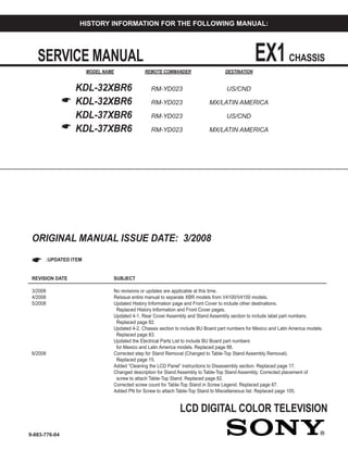
Sony kdl 32xbr6-kdl-37xbr6_chassis_ex1
1. LCD DIGITAL COLOR TELEVISION
SERVICE MANUAL EX1CHASSIS
MODEL NAME REMOTE COMMANDER DESTINATION
9-883-776-04
KDL-32XBR6 RM-YD023 US/CND
KDL-32XBR6 RM-YD023 MX/LATIN AMERICA
KDL-37XBR6 RM-YD023 US/CND
KDL-37XBR6 RM-YD023 MX/LATIN AMERICA
☛
☛
HISTORY INFORMATION FOR THE FOLLOWING MANUAL:
ORIGINAL MANUAL ISSUE DATE: 3/2008
☛ :UPDATED ITEM
REVISION DATE SUBJECT
3/2008 No revisions or updates are applicable at this time.
4/2008 Reissue entire manual to separate XBR models from V4100/V4150 models.
5/2008 Updated History Information page and Front Cover to include other destinations.
Replaced History Information and Front Cover pages.
Updated 4-1. Rear Cover Assembly and Stand Assembly section to include label part numbers.
Replaced page 82.
Updated 4-2. Chassis section to include BU Board part numbers for Mexico and Latin America models.
Replaced page 83.
Updated the Electrical Parts List to include BU Board part numbers
for Mexico and Latin America models. Replaced page 88.
6/2008 Corrected step for Stand Removal (Changed to Table-Top Stand Assembly Removal).
Replaced page 15.
Added “Cleaning the LCD Panel” instructions to Disassembly section. Replaced page 17.
Changed description for Stand Assembly to Table-Top Stand Assembly. Corrected placement of
screw to attach Table-Top Stand. Replaced page 82.
Corrected screw count for Table-Top Stand in Screw Legend. Replaced page 87.
Added PN for Screw to attach Table-Top Stand to Miscellaneous list. Replaced page 105.
2. LCD DIGITAL COLOR TELEVISION
SERVICE MANUAL EX1CHASSIS
MODEL NAME REMOTE COMMANDER DESTINATION
9-883-776-04
KDL-32XBR6 RM-YD023 US/CND
KDL-32XBR6 RM-YD023 MX/LATIN AMERICA
KDL-37XBR6 RM-YD023 US/CND
KDL-37XBR6 RM-YD023 MX/LATIN AMERICA
☛
☛
SelfDiagnosisSupported model
KDL-37XBR6 RM-YD023
3. 3KDL-32XBR6/37XBR6
KDL-32XBR6/37XBR6
TABLE OF CONTENTS
SECTION TITLE PAGE SECTION TITLE PAGE
Specifications ................................................................................. 4
Warnings and Cautions - English ................................................... 6
Warnings and Cautions - French.................................................... 7
Safety-Related Component Warning.............................................. 8
Safety Check-Out ......................................................................... 10
Self-Diagnostic Function................................................................11
SECTION 1: DISASSEMBLY............................................................... 13
1-1. Rear Cover Removal............................................................ 13
1-2. Switch Unit Removal............................................................ 13
1-3. Side Jack Bracket, BU Shield and BU Board Removal........ 14
1-4. Power Unit Removal ............................................................ 14
1-5. Table-Top Stand Removal.................................................... 15
1-6. Under Cover Removal.......................................................... 15
1-7. Structural Frames and Brackets Removal ........................... 16
1-8. LCD Panel Removal............................................................. 17
1-9. ETC- Inverter MT Board Removal (KDL-32XBR6 Only) ...... 18
1-10.ETC- Inverter MT Board Removal (KDL-37XBR6 Only) ...... 19
1-11.Speakers, Under Bar, H3E Board,
H4 Board or H4K Board, and Light Guide Removal............. 20
WIRE DRESSING ........................................................................ 21
KDL-32XBR6 Only ............................................................... 21
KDL-37XBR6 Only ............................................................... 38
SECTION 2: SERVICE ADJUSTMENTS............................................. 52
2-1. Viewing Service Adjustment Data ........................................ 52
2-2. Accessing Service Adjustment Mode................................... 52
2-3. Viewing the Service Menus.................................................. 52
2-4. Using the Remote Commander to View Service Data ......... 53
2-5. Resetting to Factory Defaults............................................... 53
SECTION 3: DIAGRAMS..................................................................... 54
3-1. Circuit Boards Location........................................................ 54
3-2. Printed Wiring Boards and
Schematic Diagrams Information......................................... 54
3-3. Block Diagram...................................................................... 56
3-4. Schematics and Supporting Information .............................. 57
BU Board Schematic Diagram (1 of 12)............................... 57
BU Board Schematic Diagram (2 of 12)............................... 58
BU Board Schematic Diagram (3 of 12)............................... 59
BU Board Schematic Diagram (4 of 12)............................... 60
BU Board Schematic Diagram (5 of 12)............................... 61
BU Board Schematic Diagram (6 of 12)............................... 62
BU Board Schematic Diagram (7 of 12)............................... 63
BU Board Schematic Diagram (8 of 12)............................... 64
BU Board Schematic Diagram (9 of 12)............................... 65
BU Board Schematic Diagram (10 of 12)............................. 66
BU Board Schematic Diagram (11 of 12)............................. 67
BU Board Schematic Diagram (12 of 12)............................. 68
G1D Board Schematic Diagram (KDL-32XBR6 ONLY) ....... 70
G2D Board Schematic Diagram (1 of 2)
(KDL-37XBR6 ONLY) .............................................. 73
G2D Board Schematic Diagram (2 of 2)
(KDL-37XBR6 ONLY) .............................................. 74
H3E Board Schematic Diagram ........................................... 77
H4 Board or H4K Board Schematic Diagram....................... 79
3-5. Semiconductors ................................................................... 81
SECTION 4: EXPLODED VIEWS........................................................ 82
4-1. Rear Cover Assembly and Table-Top Stand Assembly ....... 82
4-2. Chassis ................................................................................ 83
4-3. Connectors........................................................................... 84
4-4. Bezel Assembly and LCD Panel (KDL-32XBR6 Only)......... 85
4-5. Bezel Assembly and LCD Panel (KDL-37XBR6 Only)......... 86
4-6. Screw Legend ...................................................................... 87
SECTION 5: ELECTRICAL PARTS LIST............................................ 88
APPENDIX A: ENCRYPTION KEY COMPONENTS..........................A-1
4. 4KDL-32XBR6/37XBR6
KDL-32XBR6/37XBR6
SPECIFICATIONS
Design and specifications are subject to change without notice.
120V AC, 60Hz
160W (KDL-32XBR6 Only)
200W (KDL-37XBR6 Only)
Less than 0.1W
VIDEO (IN) 1/2/3:
S Video (4-Pin Mini DIN (VIDEO 1 Only)
Y: 1.0 Vp-p, 75 ohms unbalanced, sync negative
C: 0.286 Vp-p (Burst signal), 75 ohms
Video
1.0 Vp-p, 75 ohms unbalanced, sync negative
Audio
500 mVrms (100% modulation)
Impedance:47 kilohms
COMPONENT IN 1/2:
YPB
PR
(Component Video)
Y:1.0 Vp-p, 75 ohms unbalanced, sync negative
PB
:0.7 Vp-p, 75 ohms
PR
:0.7 Vp-p, 75 ohms
Signal format: 480i, 480p, 720p, 1080i, 1080p
AUDIO
500 mVrms (100% modulation)
Impedance: 47 kilohms
Power Requirements
Power Consumption (W)
In Use (Max)
In Standby
HDMI IN 1/2/3/4:
HDMI: Video: 480i, 480p, 720p, 1080i,1080p, 1080/24p
Audio: Two channel linear PCM 32, 44.1 and
48 kHz, 16, 20 and 24 bits, Dolby Digital
AUDIO (for HDMI IN 4):
500 mVrms (100% modulation) (Fixed)
Impedance: 47 kilohms
AUDIO OUT:
500 mVrms (+/- 3dB typical)
More than 1 Vrms at the maximum volume setting (Variable)
More than 500 mVrms (Fixed)
DIGITAL OUT (OPTICAL):
Optical Digital Audio Output (PCM/Dolby digital)
PC IN:
D-sub 15-pin, analog RGB, 0.7 Vp-p, 75 ohms, positive
PC AUDIO INPUT:
Stereo mini jack, 500 mVrms 1kh
Impedance: 47 kilohms
Trademark Information
Macintosh is a trademark of Apple Inc.,
registered in the U.S. and other countries.
HDMI, the HDMI logo and High-Definition
Multimedia Interface are trademarks or
registered trademarks of HDMI Licensing,
LLC.
Fergason Patent Properties, LLC:
U.S. Patent No. 5,717,422
U.S. Patent No. 6,816,141
Manufactured under license from Dolby
Laboratories. “Dolby” and double-D symbol
are trademarks of Dolby Laboratories.
In the United States, TV Guide and other
related marks are registered marks of
Gemstar-TV Guide International, Inc. and/or
one of its affiliates. In Canada, TV Guide is a
registered mark of Transcontinental Inc., and is
used under license by Gemstar-TV Guide
International, Inc.
The TV Guide On Screen system is
manufactured under license from Gemstar-TV
Guide International, Inc. and/or one of its
affiliates.
The TV Guide On Screen system is protected
by one or more of the following United States
patents 4,908,713; 6,498,895; 6,850,693;
6,396,546; 5,940,073; 6,239,794 to
Gemstar-TV Guide International, Inc. and/or
its subsidiaries.
Gemstar-TV Guide International Inc. and/or its
related affiliates are not in any way liable for
the accuracy or availability of the program
schedule information or other data in the TV
Guide On Screen system and cannot guarantee
service availability in your area. In no event
shall Gemstar-TV Guide International, Inc.
and/or its related affiliates be liable for any
damages in connection with the accuracy or
availability of the program schedule
information or other data in the TV Guide On
Screen system.
Blu-ray Disc is a trademark.
“BRAVIA” and , S-Force,
BRAVIA Sync, , DMex
and “x.v. Color” are
trademarks or registered marks of Sony
Corporation.
“XMB” and “XrossMediaBar” are the
trademarks of Sony Corporation and Sony
Computer Entertainment Inc.
“PLAYSTATION” is a registered trademark
and “PS3” is a trademark of Sony Computer
Entertainment Inc.
Adobe is a registered trademark or a trademark
of Adobe Systems Incorporated in United
States and/or other countries.
5. 5KDL-32XBR6/37XBR6
KDL-32XBR6/37XBR6
Television system
NTSC American TV Standard
ATSC (8VSB terrestrial) ATSC compliant 8VSB
QAM on cable ANSI/SCTE 07 2000
Channel coverage
Analog
2-69 Terrestrial
1-135 Cable
Digital
2-69 Terrestrial
1-135 Cable
Antenna
75-ohm external terminal for RF inputs
Panel System
LCD (Liquid Crystal Display) Panel
Display Resolution (horizontal x vertical)
1,920 dots x 1,080 lines
Screen Size (measured diagonally)
KDL-32XBR6 ~ 31.5 inches
KDL-37XBR6 ~ 37 inches
Supplied Accessories
Remote Commander RM-YD023
Two Size AA (R6) Batteries
HD15-HD15 Cable
Cable Holder (1 attached to the TV)
Operating Instructions
Quick Setup Guide
Installing the Wall-Mount Bracket
Warranty Card
Online Registration Card
Safety and Regulatory Booklet
Attaching the Table-Top Stand
Optional Accessories
Connecting Cables
Suport Belt Kit
Wall-Mount Bracket
SU-WL500
TV-Stand
SU-FL300/350M
in use 160W 200W
in standby
Speaker Output
mm 55 x 120 mm 58 X 126 mm
in 21/8
x 43/4
in 21/4
x 5 in
Dimensions (W x H x D)
with stand
mm 794 x 577 x 242 mm 920 x 649 x 279 mm
in 313/8
x 223/4
x 95/8
in 361/4
x 255/8
x 11 in
without stand
mm 794 x 540 x 99 mm 920 x 610 x 110 mm
in 313/8
x 213/8
x 4 in 361/4
x 241/8
x 43/8
in
wall-mount hole pattern 200 x 200 mm 300 x 300 mm
Mass
with stand
kg 15 kg 21 kg
lbs 34 lbs 47 lbs
without stand
kg 12 kg 18 kg
lbs 27 lbs 40 lbs
wall-mount screw size M6 x 12 - 18
Power Consumption
10W+10W
KDL-32XBR6 KDL-37XBR6
Less than 1W
6. 6KDL-32XBR6/37XBR6
KDL-32XBR6/37XBR6
WARNINGS AND CAUTIONS - ENGLISH
CAUTION
These servicing instructions are for use by qualified service personnel only. To reduce the risk of electric shock, do not perform any servicing other
than that contained in the operating instructions unless you are qualified to do so.
CARRYING THE TV
Be sure to follow these guidelines to protect your
property and avoid causing serious injury.
• Before carrying the TV, disconnect all cables.
• Carrying the large size TV requires two or more
people.
• When carrying the TV, place your hand as
illustrated and hold it securely. Do not subject the
TV to shocks, vibration, or excessive force.
• Lift the TV by placing your palm directly
underneath the panel but do not:
• squeeze the speaker grill area
• place your fingers in the groove above the
speaker grill area
• put stress on the LCD panel.
• Do not lift the TV from the bottom center.
WARNING!!
An isolation transformer should be used during any service to avoid possible shock hazard, because of live chassis. The chassis of this receiver is
directly connected to the ac power line.
! SAFETY-RELATED COMPONENT WARNING!!
Components identified by shading and ! mark on the schematic diagrams, exploded views, and in the parts list are critical for safe operation. Replace
these components with Sony parts whose part numbers appear as shown in this manual or in supplements published by Sony. Circuit adjustments that
are critical for safe operation are identified in this manual. Follow these procedures whenever critical components are replaced or improper operation is
suspected.
7. 7KDL-32XBR6/37XBR6
KDL-32XBR6/37XBR6
WARNINGS AND CAUTIONS - FRENCH
ATTENTION!!
Ces instructions de service sont à l’usage du personnel de service qualifié seulement. Pour prévenir le risque de choc électrique, ne pas faire
l’entretien autre que celui contenu dans le Mode d’emploi à moins que vous soyez qualifié faire ainsi.
POUR TRANSPORTER LE TÉLÉVISEUR
Assurez-vous de suivre les consignes suivantes pour
protéger votre bien et éviter les blessures graves.
• Avant de transporter le téléviseur, débranchez
tous les câbles.
• Le transport d’un téléviseur de grande taille doit
être effectué par au moins deux personnes.
• Lorsque vous transportez le téléviseur, placez vos
mains tel qu’illustré et tenez solidement
l’appareil. Ne soumettez pas le téléviseur à des
chocs ou à des vibrations, ni à une force excessive.
• Soulevez le téléviseur en plaçant la paume de votre
main directement en dessous du panneau, mais :
• n’appuyez pas sur la région de la grille de
haut-parleur
• ne placez pas vos doigts dans le sillon au-
dessus de la région de la grille de haut-parleur
• n’imposez pas de charge sur le panneau ACL.
• ne soulevez pas le téléviseur en plaçant vos
mains en dessous au centre.
Afin d’eviter tout risque d’electrocution provenant d’un chássis sous tension, un transformateur d’isolement doit etre utilisé lors de tout dépannage. Le
chássis de ce récepteur est directement raccordé à l’alimentation du secteur.
! ATTENTION AUX COMPOSANTS RELATIFS A LA SECURITE!!
Les composants identifies par une trame et par une marque ! sur les schemas de principe, les vues explosees et les listes de pieces sont d’une
importance critique pour la securite du fonctionnement. Ne les remplacer que par des composants Sony dont le numero de piece est indique dans le
present manuel ou dans des supplements publies par Sony. Les reglages de circuit dont l’importance est critique pour la securite du fonctionnement
sont identifies dans le present manuel. Suivre ces procedures lors de chaque remplacement de composants critiques, ou lorsqu’un mauvais
fonctionnement suspecte.
8. 8KDL-32XBR6/37XBR6
KDL-32XBR6/37XBR6
SAFETY-RELATED COMPONENT WARNING
There are critical components used in LCD color TVs that are important for safety. These components are identified with shading and !
mark on the schematic diagrams and the electrical parts list. It is essential that these critical parts be replaced only with the part number
specified in the electrical parts list to prevent electric shock, fire, or other hazard.
NOTE: Do not modify the original design without obtaining written permission from the manufacturer or you will void the original parts and
labor guarantee.
USE CAUTION WHEN HANDLING THE LCD PANEL
When repairing the LCD panel, be sure you are grounded by using a wrist band.
When installing the LCD panel on a wall, the LCD panel must be secured using the 4 mounting holes on the rear cover.
To avoid damaging the LCD panel:
do not press on the panel or frame edge to avoid the risk of electric shock.
do not scratch or press on the panel with any sharp objects.
do not leave the module in high temperatures or in areas of high humidity for an extended period of time.
do not expose the LCD panel to direct sunlight.
avoid contact with water. It may cause a short circuit within the module.
disconnect the AC adapter when replacing the backlight (CCFL) or inverter circuit.
(High voltage occurs at the inverter circuit at 650Vrms.)
always clean the LCD panel with a soft cloth material.
use care when handling the wires or connectors of the inverter circuit. Damaging the wires may cause a short.
protect the panel from ESD to avoid damaging the electronic circuit (C-MOS).
LEAKAGE CURRENT HOT CHECK CIRCUIT
9. 9KDL-32XBR6/37XBR6
KDL-32XBR6/37XBR6
The circuit boards used in these models have been processed using
Lead Free Solder. The boards are identified by the LF logo located
close to the board designation e.g. H1 etc [ see example ]. The
servicing of these boards requires special precautions to be taken as
outlined below.
example 1
It is strongly recommended to use Lead Free Solder material in order to guarantee optimal quality of new solder joints.
Lead Free Solder is available under the following part numbers :
Due to the higher melting point of Lead Free Solder the soldering iron tip temperature needs to be set to 370 degrees centigrade.
This requires soldering equipment capable of accurate temperature control coupled with a good heat recovery characteristics.
For more information on the use of Lead Free Solder, please refer to http://www.sony-training.com
rebmuntraP retemaiD skrameR
91-500-046-7 mm3.0 gK52.0
02-500-046-7 mm4.0 gK05.0
12-500-046-7 mm5.0 gK05.0
22-500-046-7 mm6.0 gK52.0
32-500-046-7 mm8.0 gK00.1
42-500-046-7 mm0.1 gK00.1
52-500-046-7 mm2.1 gK00.1
62-500-046-7 mm6.1 gK00.1
10. 10KDL-32XBR6/37XBR6
KDL-32XBR6/37XBR6
SAFETY CHECK-OUT
After correcting the original service problem, perform the following
safety checks before releasing the set to the customer:
1. Check the area of your repair for unsoldered or poorly soldered
connections. Check the entire board surface for solder splashes and
bridges.
2. Check the interboard wiring to ensure that no wires are “pinched” or
touching high-wattage resistors.
3. Check that all control knobs, shields, covers, ground straps, and
mounting hardware have been replaced. Be absolutely certain that
you have replaced all the insulators.
4. Look for unauthorized replacement parts, particularly transistors,
that were installed during a previous repair. Point them out to the
customer and recommend their replacement.
5. Look for parts which, though functioning, show obvious signs of
deterioration. Point them out to the customer and recommend their
replacement.
6. Check the line cords for cracks and abrasion. Recommend the
replacement of any such line cord to the customer.
7. Check the antenna terminals, metal trim, “metallized” knobs, screws,
and all other exposed metal parts for AC leakage. Check leakage as
described below.
Leakage Test
The AC leakage from any exposed metal part to earth ground and
from all exposed metal parts to any exposed metal part having a
return to chassis, must not exceed 0.5 mA (500 microamperes).
Leakage current can be measured by any one of three methods.
1. A commercial leakage tester, such as the Simpson 229 or RCA
WT-540A. Follow the manufacturers’ instructions to use these
instructions.
2. A battery-operated AC milliampmeter. The Data Precision 245
digital multimeter is suitable for this job.
3. Measuring the voltage drop across a resistor by means of a VOM
or battery-operated AC voltmeter. The “limit” indication is 0.75
V, so analog meters must have an accurate low voltage scale.
The Simpson’s 250 and Sanwa SH-63TRD are examples of
passive VOMs that are suitable. Nearly all battery-operated digital
multimeters that have a 2 VAC range are suitable (see Figure A).
How to Find a Good Earth Ground
A cold-water pipe is a guaranteed earth ground; the cover-plate
retaining screw on most AC outlet boxes is also at earth ground. If the
retaining screw is to be used as your earth ground, verify that it is at
ground by measuring the resistance between it and a cold-water pipe
with an ohmmeter. The reading should be zero ohms.
If a cold-water pipe is not accessible, connect a 60- to 100-watt
trouble- light (not a neon lamp) between the hot side of the receptacle
and the retaining screw. Try both slots, if necessary, to locate the hot
side on the line; the lamp should light at normal brilliance if the screw
is at ground potential (see Figure B).
To Exposed Metal
Parts on Set
0.15 μF
Earth Ground
AC
Voltmeter
(0.75V)
Trouble Light
AC Outlet Box
Ohmmeter
Cold-water Pipe
Figure A. Using an AC voltmeter to check AC leakage. Figure B. Checking for earth ground.
11. 11KDL-32XBR6/37XBR6
KDL-32XBR6/37XBR6
SELF-DIAGNOSTIC FUNCTION SelfDiagnosisSupported model
The units in this manual contain a self-diagnostic function. If an error occurs, the STANDBY LED indicator will automatically begin to flash. The number
of times the LED flashes translates to a probable source of the problem. A definition of the STANDBY LED flash indicators is listed in the instruction
manual for the user’s knowledge and reference. If an error symptom cannot be reproduced, the Remote Commander can be used to review the failure
occurrence data stored in memory to reveal past problems and how often these problems occur.
1. Diagnostic Test Indicators
When an error occurs, the STANDBY LED indicator will flash a set number of times to indicate the possible cause of the problem. If there is more than
one error, the indicator will identify the first of the problem areas.
Control Buttons
PIC OFF/TIMER STANDBY POWER
Description of LED Indictors
LED LED Type Description
* Light when the TV set is on
* If LED blinks continuously, this may indicate
that the TV needs servicing.
STANDBY LED
PIC OFF/
TIMER
LED
* Lights up in red when TV is in PC standby mode.
* Lights up in green when Picture Off is activated
* Lights up in orange when the timer is set
When timer is set, the LED remains lit even
when the TV is turned off.
POWER LED
Green or Orange
LED
Green LED
Red LED
12. 12KDL-32XBR6/37XBR6
KDL-32XBR6/37XBR6
2 times
5 times
LED ON 0.3 sec.
LED OFF 0.3 sec. LED OFF
3 sec.
Viewing the Self Check Diagnostic List
1. TV must be in standby mode. (Power off).
2. Press the following buttons on the Remote Commander within a second of each other:
DISPLAY Channel 5 Volume - TV POWER .
The Self Check list displays. This differs from accessing Service Adjustments.
Results for all of the following diagnostic items are displayed on screen. No error has occurred if the screen displays a “0”.
NOTE: If the Service Menu display text is not completely visible, press the Menu HOME button on the Remote Commander to refresh the display.
3. Press the Channel 1 button on the Remote Commander to go to Page 2 of the Self Check list.
SELF CHECK PAGE 1
002 MAIN_POWER 01 Í 1 indicates an error was detected
003 DC_ALERT1 00 Í 0 indicates no error was detected
005 PANEL_ALERT 00
006 BACKLIGHT 00
013 BACKLIGHT_BALANCE 00
00001 00027 00009 00000
SELF CHECK PAGE 2
007 TEMP 00
008 SP_PROT 00
011 TRIDENT_IC 00
012 HFR_ERROR 00
012 TCON_ERROR 00
00001 00027 00009 00000
4. Press the Channel 4 button on the Remote Commander to go back to Page 1 of the Self Check list.
5. To exit Self Check display, turn the power off.
Clearing the Self Check Diagnostic List
1. In Service Mode, press the Channel 8 Channel 0.
13. 13KDL-32XBR6/37XBR6
KDL-32XBR6/37XBR6
SECTION 1: DISASSEMBLY
1-1. REAR COVER REMOVAL
1 Remove Switch Unit (contains the H1 Board) from bezel
2 Disconnect 1 connector
1 Remove 2 screws from Terminal Position
2 Remove 1 screw (KDL-32XBR6 Only)
Remove 6 screws (KDL-37XBR6 Only)
3 Remove 17 screws (KDL-32XBR6 Only)
Remove 20 screws (KDL-37XBR6 Only)
1-2. SWITCH UNIT REMOVAL
Rear Cover
1
2
3
Bezel
Switch Unit (contains the H1 Board)
1
2
14. 14KDL-32XBR6/37XBR6
KDL-32XBR6/37XBR6
1-3. SIDE JACK BRACKET, BU SHIELD AND BU BOARD REMOVAL
1 Release hook and slide out Side Jack Bracket from BU Board
2 Remove 2 HEX screws
3 Disconnect 5 connectors
4 Remove 9 screws
1-4. POWER UNIT REMOVAL
1 Remove 4 screws (KDL-32XBR6 Only)
2 Disconnect 4 connectors (KDL-32XBR6 Only)
3 Remove 6 screws (KDL-37XBR6 Only)
4 Disconnect 4 connectors (KDL-37XBR6 Only)
Side Jack Bracket
BU Board
BU Shield
Main Bracket
2
4
1
3
3
1
Power Unit
(G2D Board)
G1 Bracket
Power Unit
(G1D Board)
4
2
KDL-37XBR6
KDL-32XBR6
15. 15KDL-32XBR6/37XBR6
KDL-32XBR6/37XBR6
1-5. TABLE-TOP STAND ASSEMBLY REMOVAL
1 Remove 2 screws (KDL-32XBR6 Only)
Remove 1 screw (KDL-37XBR6 Only)
1 Remove 3 screws
1-6. UNDER COVER REMOVAL
1
Table-Top Stand Assembly
Under Cover
1Under Cover
Bottom Bracket
☛
☛
16. 16KDL-32XBR6/37XBR6
KDL-32XBR6/37XBR6
1 Remove 4 screws from Top Vesa Brackets (KDL-37XBR6 Only)
2 Remove 2 screws from Top Vesa Bracket (KDL-32XBR6 Only)
3 Remove 5 screws from Main Bracket (KDL-32XBR6 Only)
Remove 3 screws from Main Bracket (KDL-37XBR6 Only)
4 Remove 2 screws from Bottom Vesa Bracket (KDL-32XBR6 Only)
Remove 6 screws from Bottom Vesa Bracket (KDL-37XBR6 Only)
5 Remove 5 screws from Spine Frames (KDL-32XBR6 Only)
Remove 6 screws from Spine Frames (KDL-37XBR6 Only)
6 Remove 2 screws from Top of Spine Frames (KDL-32XBR6 Only)
7 Remove 6 screws from Bottom Frame (KDL-32XBR6 Only)
Remove 2 screws from Bottom Frame (KDL-37XBR6 Only)
1-7. STRUCTURAL FRAMES AND BRACKETS REMOVAL
3
5
4
7
1
6
Bottom Frame
Main Bracket
Vesa (Top)
Vesa (Bottom)
Spine (R)
KDL-32XBR6
2
Vesa (Top)
Spine (L)
17. 17KDL-32XBR6/37XBR6
KDL-32XBR6/37XBR6
1 Disconnect 1 connector
2 Remove 2 screws (KDL-32XBR6)
Remove 4 screws (KDL-37XBR6 Only)
1-8. LCD PANEL REMOVAL
LCD Panel
Bezel Assembly
2
1
NOTE: The LVDS cable can only be installed one way. There is colored tape on the cable to determine which side is attached
to the TCON and which side is attached to the BU Board. Refer to Wire Dressing Illustration “Installation Procedure”
on Page 34 for KDL-32XBR6 and Page 48 for KDL-37XBR6.
1-8-1. CLEANING THE LCD PANEL
CAUTION: When cleaning the TV, be sure to unplug the power cord to avoid any chance of electric shock.
1 Clean the cabinet of the TV with a dry soft cloth.
2 Wipe the LCD screen gently with a soft cloth.
Stubborn stains may be removed with a cloth slightly moistened with a solution of mild soap and warm water.
If using a chemically pretreated cloth, please follow the instruction provided on the package.
Never use strong solvents such as a thinner, alcohol or benzine for cleaning.
Periodic vacuuming of the ventilation openings is recommended to ensure to proper ventilation.
☛
18. 18KDL-32XBR6/37XBR6
KDL-32XBR6/37XBR6
SHIELD REMOVAL BALANCER (ETC-INVERTER) BOARD REMOVAL
WARNING
NEVER REMOVE THE
SCREWS SECURING THE
PLASTIC STRIP HOLDING
THE LAMP SOCKETS
DAMAGE TO THE
BACKLIGHT TUBES WILL
Only remove the screws securing the inverter
cover which may be metal or plastic. The
remaining plastic strip contains sockets for the
fluorescent backlights and should never be
loosened. The backlights will pop out of the
sockets and/or break the backlight requiring a
LCD panel replacement.
REMOVE SCREWS
SECURING
SHIELD
REMOVE
CONNECTOR AND
PULL BOARD TO
THE RIGHT
!
.
OCCUR!
BACKLIGHT
END VIEW
SOCKET
1-9. ETC- INVERTER MT BOARD REMOVAL (KDL-32XBR6 ONLY)
1 Remove 5 screws from Board Cover.
2 Pull out the Board from Lamp socket
Balancer
(ETC- Inverter MT) Board
1
2
Inverter Board Cover
Plastic Strip
holding
Lamp Socket
DO NOT
REMOVE
BACKLIGHT
SCREWS
Balancer
(ETC- Inverter MT) Board
LCD Panel
NOTE: The LVDS cable can only be installed one way. There is colored tape on the cable to determine which side is attached
to the TCON and which side is attached to the BU Board. Refer to Wire Dressing Illustration “Installation Procedure”
on Page 34.
19. 19KDL-32XBR6/37XBR6
KDL-32XBR6/37XBR6
1
2
Balancer
(ETC- Inverter MT) Board
LCD Panel
Inverter Board Cover
SHIELD REMOVAL
NOTE:
Disconnect the 8
Inverter Board Connectors
and the LVDS Cable
before removing the Inverter Board.
REMOVE SCREWS
SECURING
SHIELD
1-10. ETC- INVERTER MT BOARD REMOVAL (KDL-37XBR6 ONLY)
1 Remove 6 screws from Board Cover
2 Disconnect 8 balancer connectors
NOTE: The LVDS cable can only be installed one way. There is colored tape on the cable to determine which side is attached
to the TCON and which side is attached to the BU Board. Refer to Wire Dressing Illustration “Installation Procedure”
on Page 48.
20. 20KDL-32XBR6/37XBR6
KDL-32XBR6/37XBR6
1 Slide out Speaker (R) unit from Bezel
2 Slide out Speaker (L) unit from Bezel
3 Remove 1 screw from Under Bar (KDL-32XBR6 Only)
Remove 2 screws from Under Bar (KDL-37XBR6 Only)
4 Disconnect 1 connector and Slide out H3E Board from Clear Panel
5 Release hooks and remove from Bezel
6 Remove 1 screw and Release hooks from Clear Panel
7 Disconnect 1 connector and Slide out H4/H4K Board from Light Guide
1-11. SPEAKERS, UNDER BAR, H3E BOARD, H4 BOARD OR H4K BOARD,
AND LIGHT GUIDE REMOVAL
Speaker Unit (L)
Speaker Unit (R)
Light Guide
Under Bar
H3E Board
H4/H4K Board
Clear Panel
2
3
1
5
4
6
7
21. 21
KDL-32XBR6/37XBR6
KDL-32XBR6/37XBR6
KDL-32XBR6 ONLY
WIRE DRESSING
HARNESS INSTALLATION ON PANEL
YELLOW TAPE IS CENTER OF PANEL. BLACK UL TAPE INDICATES WHERE HIMELON TAPE IS
APPLIED.
Use RIB on Panel as Guide where to place yellow UL tape. Apply Himelon Tape (Sheet Core C)
Over UL tape on harness.
MAKE SURE there is not a lot of excess slack on the cable when taping harness to SIDE of panel.
1 2
CAUTION
Do Not apply Sheet Core C over Yellow UL Tape
at the center of the Main Harness/Panel.
LEGEND
SHEET CORE C (2-688-011-01)
QTY=7
LCD TAPE (2-688-062-01)
QTY=6
SLIDE CLAMP (2-650-770-11)
QTY=6
22. 22
KDL-32XBR6/37XBR6
KDL-32XBR6/37XBR6
KDL-32XBR6 ONLY
LEGEND
SHEET CORE C (2-688-011-01)
QTY=7
LCD TAPE (2-688-062-01)
QTY=6
SLIDE CLAMP (2-650-770-11)
QTY=6
H Boards & Speaker Harness Use Black UL tape on harness to indicate where Himelon
(Sheet Core C) will be placed.
Apply LCD TAPE over Right speaker harness.
DO NOT block hole in speaker!
3
1
25. 25
KDL-32XBR6/37XBR6
KDL-32XBR6/37XBR6
KDL-32XBR6 ONLY
LEGEND
SHEET CORE C (2-688-011-01)
QTY=7
LCD TAPE (2-688-062-01)
QTY=6
SLIDE CLAMP (2-650-770-11)
QTY=6
HARNESS INSTALATION ON PANEL
Center of Panel
Yellow UL Tape
DO NOT APPLY Himelon
over This tape.
Apply Himelon Sheet Core C
over UL Tape on Harness
2
4
26. 26
KDL-32XBR6/37XBR6
KDL-32XBR6/37XBR6
KDL-32XBR6 ONLY
LEGEND
SHEET CORE C (2-688-011-01)
QTY=7
LCD TAPE (2-688-062-01)
QTY=6
SLIDE CLAMP (2-650-770-11)
QTY=6
HARNESS INSTALLATION ON PANEL –
CAUTION
CAUTION:
MAKE SURE ALL wires on Main Harness
are on the SIDE of the panel in this area!
If wires cross over TOP of panel, there is a
risk of DAMAGE by 3x8mm screw applied
to BU-Shield (see inset photo).
28. 28
KDL-32XBR6/37XBR6
KDL-32XBR6/37XBR6
KDL-32XBR6 ONLY
LEGEND
SHEET CORE C (2-688-011-01)
QTY=7
LCD TAPE (2-688-062-01)
QTY=6
SLIDE CLAMP (2-650-770-11)
QTY=6
BU Board support Plate
Dress Multi-Harness in 2 slide clamps as
Shown. Make sure that clamps are Locked
In T-shaped hole on BU-Bracket.
Apply Sheet Core C to Main Harness next
to 4P Speaker connector.
REVISION
5
1
2
38. 38
KDL-32XBR6/37XBR6
KDL-32XBR6/37XBR6
KDL-37XBR6 ONLY
HARNESS INSTALLATION ON PANEL
BLUE TAPE IS CENTER OF PANEL. BLACK UL TAPE INDICATES WHERE HIMELON TAPE IS
APPLIED.
Use RIB on Panel as Guide where to place BLUE UL tape. Apply Himelon Tape (Sheet Core C)
Over UL tape on harness (3places in this photo)
MAKE SURE there is not a lot of excess slack on the cable when taping to TOP of panel.
1
2
3
LEGEND
SHEET CORE C (2-688-011-01)
QTY=5
LCD TAPE (2-688-062-01)
QTY=6
SLIDE CLAMP (2-650-770-11)
QTY=7
39. 39
KDL-32XBR6/37XBR6
KDL-32XBR6/37XBR6
KDL-37XBR6 ONLY
LEGEND
SHEET CORE C (2-688-011-01)
QTY=5
LCD TAPE (2-688-062-01)
QTY=6
SLIDE CLAMP (2-650-770-11)
QTY=7
H Board & Speaker Harness
Use Black UL tape on harness to indicate where Himelon
(Sheet Core C) will be placed.
Apply LCD TAPE over Right speaker harness.
DO NOT block hole in speaker!
4
1
41. 41
KDL-32XBR6/37XBR6
KDL-32XBR6/37XBR6
KDL-37XBR6 ONLY
LEGEND
SHEET CORE C (2-688-011-01)
QTY=5
LCD TAPE (2-688-062-01)
QTY=6
SLIDE CLAMP (2-650-770-11)
QTY=7
Combination H Board/Speaker Harness
Apply LCD Tape for Left Speaker harness.
(2Places – tape over speaker not used!)
Dress Main Harness Wires in
Slide Clamp.(Revision)
3 41
2
42. 42
KDL-32XBR6/37XBR6
KDL-32XBR6/37XBR6
KDL-37XBR6 ONLY
LEGEND
SHEET CORE C (2-688-011-01)
QTY=5
LCD TAPE (2-688-062-01)
QTY=6
SLIDE CLAMP (2-650-770-11)
QTY=7BU Main Shield Plate
Dress Multi-Harness in 5 Slide Clamps as
Shown. Make sure that clamps are Locked
In T-shaped hole on BU-Bracket.
3
1
3
2
4
5
44. 44
KDL-32XBR6/37XBR6
KDL-32XBR6/37XBR6
KDL-37XBR6 ONLY
LEGEND
SHEET CORE C (2-688-011-01)
QTY=5
LCD TAPE (2-688-062-01)
QTY=6
SLIDE CLAMP (2-650-770-11)
QTY=7
Balancer Board Harness
Dress Balancer Board harness in black clips on the G Board
bracket.
Dress Balancer Board harness under black U-Clips on the G Board
bracket.
52. 52KDL-32XBR6/37XBR6
KDL-32XBR6/37XBR6
2-1. VIEWING SERVICE ADJUSTMENT DATA
There are no adjustments necessary for these models. All data has
been set for optimal viewing for our customers. The following sections
are for informational purposes only.
2-2. ACCESSING SERVICE ADJUSTMENT
MODE
1. TV must be in standby mode. (Power off).
2. Press the following buttons on the Remote Commander within a
second of each other:
DISPLAY Channel 5 Volume + POWER .
TV POWER
Onscreen cursor
and select button
DISPLAY
RM-YD023
5
VOLUME+
JUMP
The first service menu (TV) displays.
SECTION 2: SERVICE ADJUSTMENTS
TVLF CHECK
001 COLOR ADJ
001 R_DRV
SERVICE
DIGITAL PROGRAM
DATA
BE PROGRAM
NVM
PACK
BOOT
: H801.03 0070
: S001000
: TM1.000
: TD1.000
: TP1.000
: TB1.000
00100
Sample TV Service Menu
2-3. VIEWING THE SERVICE MENUS
Use the Remote Commander to view the BE and Digital service menus
options.
1. To display the Service Menu that contains the Category you want to
adjust, press JUMP on the Remote Commander.
(For a complete list of the service Categories refer to Service Menus)
NOTE: If the Service Menu display text is not completely visible, press
the Menu HOME button on the Remote Commander to refresh the
display.
Press JUMP
TVLF CHECK
001 COLOR ADJ
001 R_DRV
SERVICE
DIGITAL PROGRAM
DATA
BE PROGRAM
NVM
PACK
BOOT
: H801.03 0070
: S001000
: TM1.000
: TD1.000
: TP1.000
: TB1.000
00100
QM 0 0
INFO
SERVICE
DTV
Sample Service Menus
53. 53KDL-32XBR6/37XBR6
KDL-32XBR6/37XBR6
2-4. USING THE REMOTE COMMANDER TO
VIEW SERVICE DATA
Use the buttons on the Remote Commander to access the service menu
items and adjust the data values.
1. Access Service Mode.
Press the following buttons on the Remote Commander within a
second of each other:
DISPLAY Channel 5 Volume + POWER .
Data Value
Category
Number
Adjustment
Item Number
Category
Adjustment
Item
TVLF CHECK
001 COLOR ADJ
001 R_DRV
SERVICE
DIGITAL PROGRAM
DATA
BE PROGRAM
NVM
PACK
BOOT
: H801.03 0070
: S001000
: TM1.000
: TD1.000
: TP1.000
: TB1.000
00100
The screen displays the first category in the selected service menu.
NOTE: If the Service Menu display text is not completely visible,
press the Menu HOME button on the Remote Commander to refresh
the display.
2. To change the category, press 2 or 5 on the Remote Commander.
Note: Pressing 2 or 5 only changes the categories within the service
menu displayed.
To change a category on one of the other service menus, press the
JUMP button until the correct service menu is displayed.
3. To change the adjustment item, press 1 or 4 on the Remote
Commander.
4. To exit service mode, turn the power off.
ENT
0
Read data
from last
saved NVM
RM-YD023
5 Previous
Category
MUTING
Write into
memory
1Next item
2 Next
Category
4Previous
item
8
Restore User Control
and Channel Memory
TV POWER
JUMP
Displays
Service
Menus
2-5. RESETTING TO FACTORY DEFAULTS
Use the following instructions to restore the User Controls and
Channel Memory settings to the preset factory conditions.
1. While holding down the on the Remote Commander, press the
POWER button on the Front Panel of the set.
The set restarts and displays the initial setup screen. This may take
several minutes.
54. 54
KDL-32XBR6/37XBR6
KDL-32XBR6/37XBR6
SECTION 3: DIAGRAMS
3-1. CIRCUIT BOARDS LOCATION
3-2. PRINTED WIRING BOARDS AND SCHEMATIC DIAGRAMS INFORMATION
All voltages are in V.
S : Measurement impossibility.
: B+line.
: B-line. (Actual measured value may be different).
: signal path. (RF)
Circled numbers are waveform references.
The components identified by shading and ! symbol are critical for safety. Replace
only with part number specified.
The symbol indicates a fast operating fuse and is displayed on the component
side of the board. Replace only with fuse of the same rating as marked.
Les composants identifies per un trame et une marque ! sont critiques pour la
securite. Ne les remplacer que par une piece portant le numero specifie.
Le symbole indique une fusible a action rapide. Doit etre remplace par une
fusible de meme yaleur, comme maque.
NOTE: The components identified by a red outline and a mark contain confidential
information. Specific instructions must be adhered to whenever these components
are repaired and/or replaced.
See Appendix A: Encryption Key Components in the back of this manual.
All capacitors are in μF unless otherwise noted. pF : μμF 50WV or
less are not indicated except for electrolytics and tantalums.
All electrolytics are in 50V unless otherwise specified.
All resistors are in ohms. kΩ=1000Ω, MΩ=1000kΩ
Indication of resistance, which does not have one for rating
electrical power, is as follows: Pitch : 5mm
Rating electrical power : 1
/4
W
1
/4
W in resistance, 1
/10
W and 1
/16
W in chip resistance.
: nonflammable resistor
: fusible resistor
: internal component
: panel designation and adjustment for repair
: earth ground
: earth-chassis
All variable and adjustable resistors have characteristic curve B,
unless otherwise noted.
Readings are taken with a color-bar signal input.
Readings are taken with a 10MΩ digital multimeter.
Voltages are DC with respect to ground unless otherwise noted.
Voltage variations may be noted due to normal production
tolerances.
SWITCH UNIT (CONTAINS H1 BOARD)
POWER UNIT
(G1D KDL-32XBR6 ONLY)
(G2D KDL-37XBR6 ONLY)
H4/H4K
H3E
BU
55. 55
KDL-32XBR6/37XBR6
KDL-32XBR6/37XBR6
G
D
S
B1 E1C2
B2 C1E2
2
3
4
5
6
7
8
9
0
!¡
!™
!¢
!§
!¶
!•
–
1
G
D
S
B2 E2C1
B1 C2E1
B2 E2C1
B1 C2E1
B2 E2C1
B1 C2E1
!ª
B1 E1E2
C1(B2)C2
@º
B1E2
C1C2
@™
@£
(B2)
E1
(B2)
E1
E2B1
C2C1
@¡
B1
E1
C2
B2
C1
E2
G
S S
D
G
D
B1
E1
C2
B2
C1
E2
B1
E2
C2C1(B2)
E2
B1
C1
C2E1(B2)
C2
B1
C1
E2E1(B2)
C2
B1
C1
E2
B2
E1
C2
Ver.1.6
Transistor
(FET)
Transistor
Transistor
Transistor
Transistor
Transistor
Transistor
Transistor
Transistor
Transistor
Discrete semiconductot
(Chip semiconductors that are not actually used are included.)
Diode
Diode
Diode
Diode
Diode
Diode
Diode
Diode
Diode
Diode
Source
Source
Anode Anode
(NC)
(NC)
Cathode
Anode
Cathode
Common
Cathode Cathode
Common
Cathode Cathode
Common
Common
Common
Common
Cathode
Anode
Base Emitter
Collector
Base Emitter
Collector
Drain
Gate
Gate
Drain
Device Printed symbol Terminal name Circuit
Terminal name of semiconductors in silk screen
printed circuit ( )
Anode
Anode
Anode Cathode
Anode Anode
Cathode
!£
Transistor
(FET)
Transistor
(FET)
!?
Emitter
Collector
Base
Transistor
Source
Gate
Drain
Cathode
Anode
Anode
Cathode
Anode
Anode
*
REFERENCE INFORMATION
RESISTOR
: RN METAL FILM
: RC SOLID
: FPRD NONFLAMMABLE CARBON
: FUSE NONFLAMMABLE FUSIBLE
: RW NONFLAMMABLE WIREWOUND
: RS NONFLAMMABLE METAL OXIDE
: RB NONFLAMMABLE CEMENT
: ADJUSTMENT RESISTOR
COIL
: LF-8L MICRO INDUCTOR
CAPACITOR
: TA TANTALUM
: PS STYROL
: PP POLYPROPYLENE
: PT MYLAR
: MPS METALIZED POLYESTER
: MPP METALIZED POLYPROPYLENE
: ALB BIPOLAR
: ALT HIGH TEMPERATURE
: ALR HIGH RIPPLE
56. 56
KDL-32XBR6/37XBR6
KDL-32XBR6/37XBR6
3-3. BLOCK DIAGRAM
Tu.Tu.
x245x245
CPU
Demod.
MPEG2 Dec.
3D GPX
CC/PL
Sub Chroma
EPG(Gemstar)
USB
Ether
CXD9937GBCXD9937GB
ADC
3D Comb.
Chroma Dec.
IPC
HDMI Rx
ME/MC
YC Process
Scalar
RGB Process
PIP Process
GPX Mix
LVDS Tx
Audio
for PC
S + Video1
Video3
Component1
Audio out
(Var./Fix)
Optical
Audio Out
USB1.1
HDMI1
Component2
HDMI3
HDMI4
RF
PC (HD15)
Audio
for DVI
Rear Inputs
Video SWVideo SW
CXA2241CXA2241
( 90h )( 90h )
Video2
HDMI2
Side Inputs
CVBS
TMDS
YUV
YUV
RGB
Digital Video
ITU-R BT.656
ITU-R BT.1120
Digital GPX
RGBᔽ H/V/CLK
HV Sync/CLK
for GPX
LCD
FHD
T-Con
FHD
HFR
FHD
( 18h )
FHD Panel
with HFR
LCD
FHD
T-Con
FHD
FHD Panel
LVDS
CXD9926TPCXD9926TP
( 68h )( 68h )
Audio SW
ADC
DSP
Surround
DAC
Audio Amp.
TPA3100D2
Audio
Compound IC
SPDIFSPDIF
IIS(HDMI)
BE Micro
MB91305
[Control]
Trident
ATI
Video SW
HDMI SW
Power
TAS
HFR
CEC
Audio Mute
DDR2DDR2
32MB32MBDDR2DDR2
64MB64MB
RTCRTC
( 64h )( 64h )
One NANDOne NAND
64MB64MB
DDR2DDR2
32MB32MB
for ATSC
CVBS for PAP
for Slicer
YOUT for Slicer
HDMIHDMI
EQ_SWEQ_SW
AD8197AD8197
44 to 1to 1
( 9Eh )( 9Eh )
8bit bus
UART
IIC
IIC
IIC
TemperatureTemperature
SensorSensor
( 92h )( 92h )
IIS
ADCADC
for UI
sound
EEPROMEEPROM
32kB ( A0h )32kB ( A0h )
FlashFlash
2MB2MB
EEPROMEEPROM
8kB ( A0h )8kB ( A0h )
IIC
IIC
IIC
DDC
ECS
Buttons
SIRCS
LEDs
H3E board
H1 board
H4 board