![PHYSICAL CONFIGURATION
MOUNTING SPECIFICATIONS
FortheguidanceoftheDesignEngineer,ourapplicationslaboratoryhasgiventherecommendedpadsize&geometrywhichisshownbelow:
H-1M 1W 6.5 4.1 - - R10 1K5 0.5
H-2M 2W 9.0 4.1 - - R10 3K5 0.6
H-3AS 3W 13.0 5.7 18.0 8.00 R01 10K 1.2
H-4S 4W 15.5 6.0 19.5 8.00 R01 15K 1.5
H-5S 5W 19.5 6.5 24.5 8.25 R01 22K 2.0
H-2W 2W 13.5 Max 5.5 6.3 Min 6.0 R01 10K 0.6
HTR
TYPE
POWER
RATING
at 40°C L
±1.0
P
±1.0
DIMENSIONS (mm) RESISTANCE RANGE
min max
TYPICAL
WEIGHT
PER PC
(gms)
◊
D
(max)
D for non-inductive types and for resistance values <1R0 +0.8mm allowed.
# H for non-inductive types and for resistance values <1R0 +0.8mm allowed.
I Stands for the Impulse type resistor
F Stands for the fusible resistor as per customer request.
◊
SURFACE
MOUNT
SILICONE
COATED
TYPE
HIAS
2WS 2W 12.0 17.0 4.8 0.8 5.0 6.5 R10 5K6 0.95
2WSA 2W 9.0 13.4 4.5 0.8 4.5 6.5 R05 2K2 0.7
3WS 3W 14.5 18.7 6.0 0.8 6.5 8.0 R01 10K 1.2
3WSA 3W 13.0 18.7 5.1 0.8 6.5 6.9(max) R01 8K2 1.1
4WS 4W 15.5 20.0 6.0 0.8 8.0 8.0 R10 12K 1.25
5WS 5W 16.5 18.7 7.0 0.8 6.5 8.0 R01 12K 1.65
HTR
TYPE
POWER
RATING
at 40°C B
[±1.0]
E
[±0.5]
DIMENSIONS (mm) RESISTANCE RANGE
[min] [max]
TYPICAL
WEIGHT
PER PC
(gms)
C
[max]
A
[max]
D
[±0.05]
Z
[±1.0]
MOUNTING / ASSEMBLY DATA
For the guidance of the Design Engineer, our applications labora-
tory has given the recommended pad size and geometry which
is shown below
e : info@htr-india.com
www.htr-india.com
#
H
(max)
Rev Date : 07/01/2019
H3AS, H4S & H5S
TYPES : H2WIF
H
P
3.60 (+0.0, -0.35)
5.30 4.14.1
4.5
13.50
H-2WIF](data:image/gif;base64,R0lGODlhAQABAIAAAAAAAP///yH5BAEAAAAALAAAAAABAAEAAAIBRAA7)
Recommended
Recommended
More Related Content
What's hot
What's hot (17)
Similar to HIAS SERIES Surface Mount Wire Wound Resistors
Similar to HIAS SERIES Surface Mount Wire Wound Resistors (20)
Recently uploaded
Recently uploaded (20)
HIAS SERIES Surface Mount Wire Wound Resistors
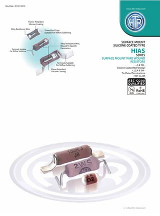
- 1. Alloy Resistance Wire Flame Retardant Silicone Coating Tinned End Caps. Suitable For Reflow Soldering Flame Ratardant Silicone Coating Terminals Suitable For Reflow Soldering Terminals Suitable For Reflow Soldering Alloy Resistance Wire, Wound To Specific Parameters • 1 & 2W - Silicone Coated Melf Design • 2,3,4 & 5W - Tin Plated Terminations • R01 to 22K SURFACE MOUNT SILICONE COATED TYPE HIAS SERIES Surface Mount Wire Wound Resistors e : info@htr-india.com www.htr-india.com Rev Date : 07/01/2019 AEC-Q200 Qualified
- 2. PHYSICAL CONFIGURATION MOUNTING SPECIFICATIONS FortheguidanceoftheDesignEngineer,ourapplicationslaboratoryhasgiventherecommendedpadsize&geometrywhichisshownbelow: H-1M 1W 6.5 4.1 - - R10 1K5 0.5 H-2M 2W 9.0 4.1 - - R10 3K5 0.6 H-3AS 3W 13.0 5.7 18.0 8.00 R01 10K 1.2 H-4S 4W 15.5 6.0 19.5 8.00 R01 15K 1.5 H-5S 5W 19.5 6.5 24.5 8.25 R01 22K 2.0 H-2W 2W 13.5 Max 5.5 6.3 Min 6.0 R01 10K 0.6 HTR TYPE POWER RATING at 40°C L ±1.0 P ±1.0 DIMENSIONS (mm) RESISTANCE RANGE min max TYPICAL WEIGHT PER PC (gms) ◊ D (max) D for non-inductive types and for resistance values <1R0 +0.8mm allowed. # H for non-inductive types and for resistance values <1R0 +0.8mm allowed. I Stands for the Impulse type resistor F Stands for the fusible resistor as per customer request. ◊ SURFACE MOUNT SILICONE COATED TYPE HIAS 2WS 2W 12.0 17.0 4.8 0.8 5.0 6.5 R10 5K6 0.95 2WSA 2W 9.0 13.4 4.5 0.8 4.5 6.5 R05 2K2 0.7 3WS 3W 14.5 18.7 6.0 0.8 6.5 8.0 R01 10K 1.2 3WSA 3W 13.0 18.7 5.1 0.8 6.5 6.9(max) R01 8K2 1.1 4WS 4W 15.5 20.0 6.0 0.8 8.0 8.0 R10 12K 1.25 5WS 5W 16.5 18.7 7.0 0.8 6.5 8.0 R01 12K 1.65 HTR TYPE POWER RATING at 40°C B [±1.0] E [±0.5] DIMENSIONS (mm) RESISTANCE RANGE [min] [max] TYPICAL WEIGHT PER PC (gms) C [max] A [max] D [±0.05] Z [±1.0] MOUNTING / ASSEMBLY DATA For the guidance of the Design Engineer, our applications labora- tory has given the recommended pad size and geometry which is shown below e : info@htr-india.com www.htr-india.com # H (max) Rev Date : 07/01/2019 H3AS, H4S & H5S TYPES : H2WIF H P 3.60 (+0.0, -0.35) 5.30 4.14.1 4.5 13.50 H-2WIF
- 3. 2WS 2.5 5.5 14.0 2WSA 2.5 (min) 5.5 (min) 10.0 (max) 3WS 2.5 (min) 8.0 (min) 15.0 (max) 3WSA 2.5 (min) 8.0 (min) 15.0 (max) 4WS 2.5 9.5 17.0 5WS 2.5 (min) 8.0 (min) 15.0 (max) HTR TYPE DIMENSIONS (mm) a b l SURFACE MOUNT SILICONE COATED TYPE HIAS ELECTRICAL AND ENVIRONMENTAL CHARACTERISTICS / DATA Power Rating Subject to size of solder pads used and type (Rated Ambient Temperature) of PCB / pads (Performance requirements shown are based on use of FR4 test boards measuring 50mm x 50mm with 300g/m² copper pads) Resistance Tolerances Available JIS-C-5202- Para 5.1 Operating Temperature Range Voltage Rating / Limiting V = PxR Voltage / Max Working Voltage Maximum Overload Voltage (Pulse) IEC 6100-4-5 (1.2/50µsec) Rated load JIS-C-5202- Para 5.4 Voltage Proof /Dielectric JIS-C-5202- Para 5.7 (based on limiting Withstanding Voltage voltage x 2 or 500V whichever is applicable) Temperature Rise Will vary based on solder pad dimensions used Short Time Overload JIS-C-5202- Para 5.5 (upto 3W - condition A - R.V x 2.5 for 5 secs) (4W and above - condition B - voltagecorrespondingto10timespowerfor5secs) Insulation Resistance JIS-C-5202- Para 5.6 (condition F) Temperature Co-efficient of JIS-C-5202- Para 5.2 Resistance Endurance - under load with JIS-C-5202- Para 7.9 humidity 1000 hours at 40°C ± 2°C, 95%, R.H with limiting voltage - 1.5 hours on / 0.5 hours off Damp Heat (Steady State) JIS-C-5202- Para 7.5 Temperature Cycling JIS-C-5202- Para 7.4(Roomtemperature→-55°C→ Room temperature→155°C→ Room temperature for 5 cycles) Load Life JIS-C-5202- Para 7.10 1000 hours at 70°C with limiting voltage - 1.5 hours on / 0.5 hours off Climate Category Solvent Resistant JIS-C-5202- Para 6.9 Solvent A - 1PA for 60 secs ± 10 secs Flame Retardant JIS-C-5202- Para 7.12.3.2 (under overload condition) Full power dissipation at 40°C and linearly derated to zero at 275°C (Refer derating curve shown) ±10% [K]; ±5% [J]; ±3% [H]; ±2%[G]; ±1% [F] -55°C to +275°C (with suitable derating as per derating curve shown) Varies depending on resistance value, duration between pulses & no. of pulses to be withstood (contact factory for details) ∆R ± [1% + R05] ∆R ± [1% + R05] Consult factory with full details of pad size used ∆R ± [1.2% + R05] - Average > 1000M.Ω (dry) ± 90 ppm/°C [>10R] ± 80 ppm/°C [<10R] ± 200 ppm/°C [<R10] ∆R ± [5% + R05] ∆R ± [3% + R05] ∆R ± [2% + R05] - Typical ∆R ± [≤3% + R05] - Average 55/200/56 No effect on coating or marking No flaming / arcing PARAMETER/ PERFORMANCE TEST TEST METHOD - DETAILS PERFORMANCE REQUIREMENTS e : info@htr-india.com www.htr-india.com Rev Date : 07/01/2019
- 4. SURFACE MOUNT SILICONE COATED TYPE HIAS MECHANICAL SPECIFICATIONS TYPICAL APPLICATIONS This series has been evolved in order to fill the gap for melf and surface mount resistors in applications which are too severe for film resistors. The advantages are superior power to size zero ratio, higher tolerance to pulse, surge applications and negligible noise. ORDERING INFORMATION For RoHS version - H3AS * PARAMETER/ PERFORMANCE TEST TEST METHOD - DETAILS PERFORMANCE REQUIREMENTS Resistance to Soldering Heat 260°C - 270°C for 10 secs. Solderability JIS-C-5202- Para 6.5 ∆R ± [0.75% + R05] - Typical Continuous and satisfactory (95% min coverage). Series HTR Type Packing Resistance Value Tolerance HIAS H3AS / H3AS* Bulk H3AS / H3AS* 100R J e : info@htr-india.com www.htr-india.com Rev Date : 07/01/2019