1. Design Rules Reference
Summary This comprehensive reference provides detailed information on setting up design rules
for a PCB design. It also covers addition of rule-based parameters to objects in the
Technical Reference schematic and Design Rule Checking. Detailed information for each of the individual
TR0116 (v1.8) May 20, 2008 rule types and their associated constraints is also provided.
PCB design is no longer a matter of placing tracks to create connections. High speed logic combined with smaller and more
complex packaging technologies place new demands on the PCB Designer. It is not possible to satisfy all the requirements of
the design by only considering the clearance between tracks, pads and vias. Designs today can also require that you apply
specific requirements to individual nets, components or regions of the board as well as considering such issues as crosstalk,
reflections and net lengths. Altium Designer's PCB Editor allows you to define design rules that monitor and test for these and
other requirements.
Design rules collectively form an instruction set for the PCB Editor to follow. Each rule represents a requirement of your design
and many of the rules, eg. clearance and width constraints, can be monitored as you work by the online Design Rule Checker
(DRC). Certain rules are monitored when using additional features of the software, for example routing-based rules when using
the Situs Autorouter to route a design, or signal integrity-based rules used by the Signal Integrity Analyzer when performing a
detailed signal integrity analysis of a design.
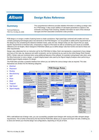
The PCB Editor provides a powerful interface from where you can define the various design rules as required. The rules
themselves are divided into the following categories:
• Electrical
• Placement PCB Design Rules
• Routing
• Manufacturing Electrical Routing SMT Mask Signal Integrity
• SMT Clearance Width SMD to Corner Solder Mask Signal Stimulus
Routing Topology Expansion Overshoot -
• Plane Short-Circuit SMD to Plane
Paste Mask Falling Edge
Un-Routed Net Routing Priority SMD to Neck-Down
• Mask Expansion Overshoot -
Un-Connected Pin Routing Layers Rising Edge
• Testpoint Routing Corners
Plane Undershoot -
• High Speed Routing Via Style
High Speed Falling Edge
Placement Power Plane
• Signal Integrity. Room Definition Fanout Control Connect Style Parallel Segment Undershoot -
Length Rising Edge
Component Differential Pairs Power Plane
Clearance Routing Clearance Matched Net Impedance
Polygon Connect Lengths Signal Top Value
Component
Orientations Style Daisy Chain Stub
Manufacturing Signal Base Value
Length
Permitted Layers Minimum Annular Flight Time -
Vias Under SMD Rising Edge
Nets to Ignore Ring Testpoint
Maximum Via Flight Time -
Height Acute Angle Testpoint Style Count Falling Edge
Hole Size Testpoint Usage Slope -
Layer Pairs Rising Edge
Slope -
Falling Edge
Supply Nets
With a well-defined set of design rules, you can successfully complete board designs with varying and often stringent design
requirements. This is further enhanced by the fact that the PCB Editor allows you to export and import rule sets, enabling you
to store and retrieve your favorite design rule configurations, depending on the job at hand.
TR0116 (v1.8) May 20, 2008 1
2. Design Rules Reference
Creating and Editing Design Rules in the PCB Document
To set up new design rules or edit existing ones
for the current design, from the PCB document
select Design » Rules to open the PCB Rules
and Constraints Editor dialog.
In the folder-tree pane on the left side of the
dialog, each of the ten design rule categories
are listed under the Design Rules folder. Click
on the root folder (Design Rules) to access a
summary listing - in the main editing window of
the dialog - of all specific rules that have been
defined for all design rule types, across all
categories (as shown in the previous image).
Click on a category to list all specific rules that
have been defined for all associated design rule
types of that category.
Click on a rule type to list all specific rules that have been defined for that type.
In each case - whether you have clicked on the root folder, a category or a type - the main editing window of the dialog will
display the following summary information for each defined rule:
• the rule name
• the type of rule it is
• the rule category it belongs to
• the scope of the rule (i.e. what object(s) it applies to)
• the constraint attributes that have been defined for the rule
• the rule's priority.
You can also enable/disable a rule from within these summary list views.
2 TR0116 (v1.8) May 20, 2008
3. Design Rules Reference
Creating a New Rule
A new rule can be created by right-clicking on the
required rule type in the folder-tree pane and choosing
New Rule from the pop-up menu.
Alternatively, pressing the Rule Wizard button at the
bottom of the dialog will launch the New Rule Wizard.
Follow the pages in this wizard to quickly create a new
design rule of any type
The new rule will be added to the folder-tree and will
also appear in the summary list for that rule type. The
rule name will appear bold to distinguish it as being
new and yet to be 'applied'.
Editing a Rule
To edit the scope and constraint attributes for a rule,
either click on the entry for the rule in the folder-tree
pane or double-click on its entry in a summary list. The
main editing window of the dialog will change to give
access to the controls for defining the scope and
constraint attributes for that rule. The example image
below shows the controls accessed for a Solder Mask
Expansion rule.
Changes made to existing rule definitions are
highlighted in both the folder-tree pane and the
applicable summary lists. Such entries are
distinguished by the rule name becoming bold and an
asterisk displayed to the right of the name. The asterisk
is used to reflect that the rule is an existing rule that
has been modified, rather than a newly created rule (which is displayed bold without an asterisk).
TR0116 (v1.8) May 20, 2008 3
4. Design Rules Reference
Deleting a Rule
To delete a design rule, right-click on its entry in the folder-tree pane of the PCB Rules and Constraints Editor dialog and
choose the Delete Rule command from the pop-up menu that appears.
The rule name will appear bold with strike-through highlighting to distinguish it as being a
deletion that is yet to be 'applied'.
Effecting Rule Changes
To effect changes, either press the Apply button or press OK. Use of the former will allow you stay in the dialog to carry out
further changes.
Notes
When a new rule is added from within the PCB Rules and Constraints Editor dialog it will initially be given a default name based
on the specific type of rule. For example, if you add a new Clearance rule, the default name will be Clearance. If this default
naming is not changed, adding another new rule of the same type will result in the same rule name with an incremented
numerical suffix (i.e. Clearance_1, Clearance_2, and so on).
When a new rule is created for a particular rule type, it is automatically given priority 1. If any other rules of that type exist, their
priorities will be shifted, by one, accordingly. They are then considered to be modified - even though you may not have
specifically modified them at the scope/constraint level. All such existing rules of that type will therefore be displayed in the
modified state (bold with asterisk).
If you do not want to use a design rule, but may wish to use it in the future, rather than delete it you can disable it. Toggle the
corresponding Enable option for the rule in one of the relevant summary lists.
Many rule types have default rules created when you open a new PCB document. In a similar fashion, if you delete all specific
rules for one of those rule types, the default rule will be re-added automatically. For information on the default rules that are
created, see the Default Design Rules Created with a New PCB Document topic.
4 TR0116 (v1.8) May 20, 2008
5. Design Rules Reference
Defining the Scope of a Design Rule
When defining the scope of a design rule - the extent of
its application - you are essentially building a query to
define the member objects that are governed by the
rule. Use the options available in the dialog to build the
query required.
Depending on whether the rule is unary or binary, you
will need to define one or two scopes respectively. For more information, see the Unary and Binary Design Rules topic.
Basic options allow you to quickly generate scope queries that target:
• all design objects
• all objects in a specific net
• all objects in a specific net class
• all objects on a specific layer
• all objects in a specific net and on a specific layer.
The available drop-down fields will populate in accordance with the basic option chosen. When using the Net, Net Class or
Layer option, use the top drop-down field to choose from:
• all defined nets in the design,
• all defined net classes in the design or
• all currently enabled layers in the design, respectively.
When using the Net and Layer option, the top drop-
down will contain the list of nets in the design, with the
bottom drop-down containing the list of enabled layers.
As you select an option, the corresponding query will
appear in the Full Query region of the dialog.
The Advanced (Query) option enables you to write
your own, maybe more complex, but also more specific
query. Two facilities are available to provide aid in the creation of queries - the Query Builder and the Query Helper. These
facilities can be very useful if you are unsure of the syntax of a query or the possible keywords that you may want to use.
Using the Query Builder
Click the Query Builder button to open the Building Query from Board
dialog, which enables you to create a query for targeting specific
objects in the design document, by simple construction of a string of
ANDed and/or ORed conditions.
The left-hand section of the dialog is where you specify the
condition(s) that you require to target the set of objects needed.
Initially the entry in the Condition Type/Operator column will be Add
first condition. Clicking on this field will reveal a list of condition
types.
The condition types listed will only reflect those relevant to building the scope for
the current rule type.
Choose the first condition and click in the Condition Value column to access a
drop-down list of possible values for that condition type. As you define a condition
in the left-hand section of the dialog, a preview of the currently built query is shown
in the right-hand section.
Continue to add further conditions to narrow down your
target set of design objects as required. Conditions can be
ANDed or ORed together. The default logical operator is
AND. To change the logical operator between conditions,
click on the AND or OR entry in the Condition
Type/Operator column and select the required operator.
TR0116 (v1.8) May 20, 2008 5
6. Design Rules Reference
The preview of the query will update accordingly.
When the expression for the query has been defined as required,
clicking OK will load the expression into the Full Query region of the
PCB Rules and Constraints Editor dialog. Note that the scope option
will automatically be switched to Advanced (Query).
Specifying Precedence
The and buttons at the top of the dialog essentially allow you to add and remove brackets around the presently
selected condition (increasing and decreasing indent). This allows you to create precedence for certain logically ANDed or
logically ORed conditions. For example, consider the following query:
(InNet('+12V') AND (OnLayer('TopLayer') AND IsTrack))
In this case, the first condition has been set to the
condition type Belongs to Net, with value +12V.
Another condition has then been added, using the
condition type Exists on Layer, with the value
TopLayer.
At this stage, with the second condition selected in the
dialog, the right arrow button has been clicked.
Brackets have been added around the second
condition and now the possibility to add a condition
within that pair of brackets is given.
The third condition with condition type Object Kind
and value Track is then added within the brackets.
Use the Show Level list to control the display of levels in your structured string of conditions, essentially expanding/collapsing
the display of brackets. Adding brackets creates a new level. You can display levels 1-5. For any further levels added, use the
Show All Levels option. Alternatively, click on the expand (+) or contract (-) symbols (associated with a bracketed condition) to
6 TR0116 (v1.8) May 20, 2008
7. Design Rules Reference
show the next level(s) or hide the current level (and all levels below) respectively. The and buttons can also be used to
expand or collapse the currently selected condition.
Use the and buttons to move a selected condition in the query string being built. For a condition that has sub-levels (i.e.
a bracketed condition), any condition in the level structure can be moved. When levels are expanded, a condition can be moved
down or up through the levels. When levels are collapsed, a condition will be moved over the level structure.
To delete a condition, select it and either click the button, or use the Delete key.
Using the Query Helper
To use the Query Helper, ensure that the Advanced (Query)
option is enabled and then click on the Query Helper button to
open the Query Helper dialog. The underlying query engine
analyzes the PCB design and lists all available objects, along
with generic keywords for use in queries.
Use the Query region of the dialog to compose a query
expression. You can type directly within the region. As you type,
a context-sensitive prompt list of possible keywords or objects
will appear as an aid.
The Categories region of the dialog provides
access to available PCB Functions, PCB Object
Lists and System Functions, which can be used
to create the query expression. As you click on a
sub-category within each of these three areas,
the corresponding list of keywords or objects will
be displayed in the region to the right.
Locate the keyword or object that you wish to use
in the query string, using the Mask field if need
be, and then double-click on the entry. The entry
in the Name column will be inserted at the cursor
position in the Query region of the dialog.
The mid-section of the dialog provides a range of
operators (as buttons) for use when constructing
an expression. Use the Check Syntax button to
verify that an expression is syntactically correct.
When the expression for the query has been
defined as required, clicking OK will load the
expression into the Full Query region of the PCB
Rules and Constraints Editor dialog.
TR0116 (v1.8) May 20, 2008 7
8. Design Rules Reference
Notes
You can type your own specific query for the rule scope directly into the Full Query region of the PCB Rules and Constraints
dialog, or elaborate on one of the basic query entries. In either case, the Query Kind option will change to Advanced (Query)
and access to the Query Helper dialog will be made available, should you wish or need to use it.
The Query Builder (Building Query from Board dialog) is a simpler method of constructing a query, using sensitive condition
types and values that only allow you to build using relevant 'building blocks'. For advanced query construction, with full keyword
specification and operator syntax, use the Query Helper dialog.
When using the Query Helper dialog to construct a query, clicking inside a typed keyword or on a keyword in one of the
available lists and pressing F1, will launch help for that particular keyword.
When using the Query Builder:
• You can adjust any condition in your query string, at any time, by clicking on the entry for that condition in the Condition
Type/Operator column and choosing the required new condition from the available entries in the drop-down list. The
preview of the query expression will update accordingly
• The currently selected condition or logical operator in the left side of the dialog is visually confirmed in the preview section of
the dialog by the entry appearing in red text
• The CTRL + Up Arrow and CTRL + Down Arrow keyboard shortcuts can also be used to move the selected condition entry
up or down in the structure respectively
• The CTRL + Right Arrow and CTRL + Left Arrow keyboard shortcuts can also be used to increase or decrease indent at
the selected position in the structure (add/remove brackets) respectively.
When building query expressions using the Query Helper:
• It is highly advisable to use brackets whenever there is any possibility whatsoever that the query might not be correctly
interpreted
• Brackets have the highest precedence within an order of precedence that has been defined for the various operators
provided and which determines how queries are interpreted by the software (whenever the user has not provided brackets).
The sequence of this order is as follows:
Brackets
Not
^, *, /, Div, Mod, And
+, -, Or, Xor
=, <>, <, >, <=, >=
&&, ||
This order of precedence is similar to that used in Pascal type languages. However, generous usage of brackets removes
doubt and makes the resulting queries easier to read by others
• Ambiguities are resolved by working from left to right
• Parentheses are evaluated from inside to outside and equal levels are done left to right
The rule scope (Full Query) is checked automatically. If you switch from a rule with an
incorrectly defined scope to another rule, the former will appear highlighted in red in the folder-
tree pane of the dialog.
Similarly, if you close the PCB Rules and Constraints Editor dialog and rules with incorrect
scope definitions exist, a dialog will appear alerting you to this fact and asking if you wish to
correct them. If you click Yes, the folder-tree pane will be fully expanded, enabling you to
glance down and easily catch the offending, red-highlighted rules.
8 TR0116 (v1.8) May 20, 2008
9. Design Rules Reference
Browsing Rules using the PCB Panel
A list of currently defined rules can be displayed in the PCB panel by enabling the Rules mode for the panel.
All rules can be viewed or only those rules associated with a particular rule type. The Rule Classes region will only include a
rule type if a specific rule of that type has been defined for the active design.
Double-clicking on a rule entry (or right-clicking on a rule entry and selecting Properties from the pop-up menu) will open the
relevant Edit PCB Rule dialog, from where you can edit the scope of the rule and also the specific rule constraints.
As you click on a specific rule in the Rules region of the panel, filtering will be applied, using the rule as the scope of the filter.
Only those design objects that fall under the scope of the rule will be filtered, the visual result of which (in the main design
window) is determined by the highlighting options enabled (Mask/Dim/Normal, Select, Zoom). Multiple rule entries can be
selected using standard SHIFT + Click and CTRL + Click features.
This allows you to examine which objects an enabled rule
applies to when creating your query for the rule scope(s).
Because you can edit a rule directly from the panel, you can
tweak your query until the desired objects are captured by
the scope(s).
For more information about the PCB panel, press F1 when
the cursor is over the panel.
TR0116 (v1.8) May 20, 2008 9
10. Design Rules Reference
Unary and Binary Design Rules
There are two types of design rules - unary and binary. Unary rules apply to one object, or each object in a set of objects. As a
consequence, unary design rules have one rule scope. Binary rules apply between two objects, or between any object in one
set to any object in a second set. As a consequence, binary design rules have two rule scopes.
An example of a unary rule is the Solder Mask Expansion rule. This rule applies individually to each pad identified by the rule
scope.
An example of a binary rule is the Clearance rule, which applies between any copper object in the first set and any copper
object in the second set, as identified by the separate queries of the two rule scopes.
Viewing Applicable Unary Rules
For any placed object in the current design, you can quickly access information about which unary design rules apply to that
object. Position the cursor over the object (or select it), right-click and select Applicable Unary Rules from the pop-up menu.
The Applicable Rules dialog will appear.
All defined design rules that could
be applied to the selected object are
analyzed and listed in the dialog.
The specific constraints for each rule
are also displayed.
Each rule that is listed in the dialog
will have either a tick ( ) or a cross
( ) next to it. A tick indicates that
this is the rule with the highest
priority out of all applicable rules of
the same type and is the rule
currently applied. Lower priority
rules of the same type are listed with
a cross next to them, indicating that
they are applicable but, as they are
not the highest priority rule, they are
not currently applied.
Any rules that would apply to the
object but are currently disabled also
have a cross next to them and are
shown using strike through
highlighting.
10 TR0116 (v1.8) May 20, 2008
11. Design Rules Reference
Viewing Applicable Binary Rules
In a similar fashion, you can also access information about the binary design rules that apply between two placed objects in a
design. Position the cursor over any object, right-click and select Applicable Binary Rules from the pop-up menu. You will be
prompted to select two objects in the design. Position the cursor over each object in turn and click or press ENTER. The
Applicable Rules dialog will appear, displaying all binary design rules that apply to those objects.
Note: If the two objects that you select do not have any binary rules applied to them, the Applicable Rules dialog will not open.
Notes
If, rather than seeing which rules apply to an object (or between two objects) you would prefer to pick a rule and see which
objects that rule applies to, this can be achieved from the PCB panel, when configured in Rules mode. As you click on a
specific rule in the Rules region of the panel, filtering will be applied, using the rule as the scope of the filter. Only those design
objects that fall under the scope of the rule will be filtered, the visual result of which (in the main design window) is determined
by the highlighting options enabled (Mask/Dim/Normal, Select, Zoom).
For more information about the PCB panel, press F1 when the cursor is over the panel.
TR0116 (v1.8) May 20, 2008 11
12. Design Rules Reference
Rule Priority
As you create a new rule, it is given a priority setting. This setting defines the order in which multiple rules of the same type are
applied when, for example, performing a Design Rule Check.
Each new rule you add for the same rule type, will be given the highest priority setting, i.e. 1. You can change the priority order
that exists for rules of the same type by clicking
on the Priorities button in the PCB Rules and
Constraints Editor dialog. The Edit Rule
Priorities dialog opens.
Initially, the dialog will list all rule instances for
the rule type that is currently selected in the
PCB Rules and Constraints Editor dialog. Use
the Rule Type field to change the rule type and
hence list the specific rules defined for that type.
The defined rules are listed in order of current
priority - from 1 (highest priority) downwards.
Select a rule entry and use the Increase
Priority and Decrease Priority buttons to move
it up or down in the priority order respectively.
Notes
Multiple rules of the same type can be set up. It may arise that a design object is covered by more than one rule with the same
scope. In this instance, a contention exists. All contentions are resolved by the priority setting. The system goes through the
rules from highest to lowest priority and picks the first one whose scope expression(s) match the object(s) being checked.
When a new rule is created for a particular rule type, it is automatically given priority 1. If any other rules of that type exist, their
priorities will be shifted (lowered), by one, accordingly. They are then considered to be modified - even though you may not
have specifically modified them at the scope/constraint level. All such existing rules of that type will therefore be displayed in the
modified state (bold with asterisk).
12 TR0116 (v1.8) May 20, 2008
13. Design Rules Reference
Application of Design Rules
Different design rules are applied in different situations. Certain rules can be applied as you design, by enabling the online
design rule check (DRC) feature. A violation of a rule is flagged as soon as the violation occurs during placement. You may
prefer to design first and check for violations later. If this is the case, you could enable the batch DRC feature, which will apply a
certain set of rules when launched and provide feedback via a report. Some rules are only applied at certain times and during
software operations, such as autorouting, autoplacement and manufacturing output generation.
The PCB Editor only applies each rule when it is appropriate. A rule's definition specifies when that particular rule is applied. To
reiterate, each rule is applied in one or more of the following situations:
• Online Design Rule Check (DRC): running in the background, as you work, flagging and/or automatically preventing design
rule violations of certain rule types
• Batch DRC: allows you to manually run a DRC at any time during the board design process, on all enabled rule types, and
obtain a report
• During a software operation: certain rules are monitored during a software operation including: polygon pour, autorouting,
autoplacement and output generation. Examples of these include the mask expansion rule which is monitored during output
generation and the routing via style rule which is monitored during autorouting.
The following table summarises where each of the individual rule types are applied:
Auto- Online Batch Output
Rule Category router DRC DRC Generation Other
Clearance Electrical Interactive routing, Polygon placement
Short-Circuit Electrical
Unrouted Net Electrical
Unconnected Pin Electrical
Parallel Segment High Speed
Length High Speed
Matched Net Lengths High Speed Equalize Net Lengths command
Daisy Chain Stub Length High Speed
Vias Under SMD High Speed
Maximum Via Count High Speed
Minimum Annular Ring Manufacturing
Acute Angle Manufacturing
Hole Size Manufacturing
Layer Pairs Manufacturing Interactive routing
Solder Mask Expansion Mask
Paste Mask Expansion Mask
Room Definition Placement Arrange Within Room command
Component Clearance Placement Autoplacement (Cluster Placer)
Component Orientations Placement Autoplacement (Cluster Placer)
Permitted Layers Placement Autoplacement (Cluster Placer)
Nets to Ignore Placement Autoplacement (Cluster Placer)
Height Placement Autoplacement PCB3D Editor
Power Plane Connect Style Plane Internal Planes
Power Plane Clearance Plane Internal Planes
TR0116 (v1.8) May 20, 2008 13
14. Design Rules Reference
Auto- Online Batch Output
Rule Category router DRC DRC Generation Other
Polygon Connect Style Plane Polygon placement
Broken plane Plane Additional split plane error report
Dead Copper Plane Additional split plane error report
Starved Thermal Plane Additional split plane error report
Width Routing Interactive routing
Routing Topology Routing
Routing Priority Routing
Routing Layers Routing
Routing Corners Routing Third party Autorouters (e.g. Specctra)
Routing Via Style Routing Interactive routing
Fanout Control Routing Interactive routing
Differential Pairs Routing Routing Interactive routing
Signal Stimulus Signal Integrity Signal Integrity Analysis
Overshoot - Falling Edge Signal Integrity Signal Integrity Analysis
Overshoot - Rising Edge Signal Integrity Signal Integrity Analysis
Undershoot - Falling Edge Signal Integrity Signal Integrity Analysis
Undershoot - Rising Edge Signal Integrity Signal Integrity Analysis
Impedance Signal Integrity Signal Integrity Analysis
Signal Top Value Signal Integrity Signal Integrity Analysis
Signal Base Value Signal Integrity Signal Integrity Analysis
Flight Time - Rising Edge Signal Integrity Signal Integrity Analysis
Flight Time - Falling Edge Signal Integrity Signal Integrity Analysis
Slope - Rising Edge Signal Integrity Signal Integrity Analysis
Slope - Falling Edge Signal Integrity Signal Integrity Analysis
Supply Nets Signal Integrity Signal Integrity Analysis
SMD To Corner SMT
SMD To Plane SMT
SMD Neck-Down SMT
Testpoint Style Testpoint Find and Set Testpoints command
Testpoint Usage Testpoint Find and Set Testpoints command
14 TR0116 (v1.8) May 20, 2008
15. Design Rules Reference
Design Rule Checking (DRC)
Design Rule Checking (DRC) is a powerful automated feature that checks both the logical and physical integrity of your design.
Checks are made against any or all enabled design rules and can be made online, as you work, and/or as a batch check, with
results listed in the Messages panel and a generated report. This feature should be used on every routed board to confirm that
minimum clearance rules have been maintained and that there are no other design violations. It is particularly recommended
that you always perform a design rule check prior to generating final artwork.
Configuring the DRC
Configuration for the check is carried out in the Design Rule
Checker dialog, accessed by selecting the Design Rule
Check command from the PCB Editor's Tools menu.
In the folder list on the left side of the dialog, each of the design
rule categories whose rule types can be checked are listed
under the Rules To Check folder. Click on the Rules To
Check folder to list all checkable design rule types, across all
categories, in the right side of the dialog.
Click on a category to list all associated (and checkable) design
rule types for that category.
Enable/disable Online (where available) and/or Batch checking
options for each rule type you wish to
check. Use the options available from
the right-click pop-up menu to
enable/disable checks of all rule types,
or to enable checks of all used rule types
only.
TR0116 (v1.8) May 20, 2008 15
16. Design Rules Reference
Using Online DRC
To turn on the Online DRC feature, enable the Online DRC option on the
PCB Editor - General page of the Preferences dialog (Tools »
Preferences). Online Design Rule Checking runs in the background, as
you work, flagging and/or automatically preventing design rule violations.
Errors are highlighted in the document by outlining the violating object(s) in
the current DRC Error Markers color, defined in the System Colors region
of the View Configurations dialog (Design » Board Layers & Colors).
Using Batch DRC
Batch Design Rule Checking allows you to manually run
a check at any time during the board design process.
When setting up a batch DRC, various additional options
can be defined by clicking on the Report Options folder,
in the folder-tree pane of the Design Rule Checker
dialog. These options include generation of a report.
A batch DRC is initiated by clicking the Run Design Rule
Check button, at the bottom left of the dialog. After the
check has completed, all violations will appear listed as
messages in the Messages panel.
If the Create Violations report option is enabled,
clearance, length and width errors will be highlighted on
the PCB document.
DRC Reports
Enable the Create Report File option in the Design Rule Checker dialog to generate a DRC report. Options available on the
PCB Editor - Reports page of the Preferences dialog allow you to specify in which format the report is generated and whether
a report is automatically displayed in the main design window. The following report formats are available:
• TXT - producing the Design Rule Check - PCBDocumentName.drc file
• HTML - producing the Design Rule Check - PCBDocumentName.html file
• XML - producing the PCBDocumentName.xml file.
By default, TXT and HTML formats are generated, with the HTML report being displayed after generation.
16 TR0116 (v1.8) May 20, 2008
17. Design Rules Reference
The report lists each rule that was tested, as
specified in the Design Rule Checker dialog. Each
violation that was located is listed with full details of
any reference information, such as the layer, net
name, component designator and pad number, as
well as the location of the object. In the HTML format
report, click on the entry for an offending object to
cross probe directly to that object in the workspace.
Interrogating Design Violations
There are essentially three methods of interrogating
design violations - from the Messages panel, from
the PCB panel and directly within the design
workspace. The first method is solely associated with
having run a Batch DRC.
From the Messages Panel
After running a Batch DRC, double-clicking a
violation message in the Messages panel will cross
probe to the object(s) causing that violation in the
main design window. Note: The Create Violations
option must be enabled as part of the DRC Report
options in the Design Rule Checker dialog, for the
cross probing to work.
From the PCB Panel
When running an Online or Batch DRC,
any rule violations associated with a rule
class or individual rule will be listed in the
Violations region of the PCB panel, when
the panel is configured in Rules mode.
Clicking on a violation entry will apply
filtering using the offending object(s) as
the scope of the filter. The resulting view
in the main design window will depend on
the highlighting options enabled
(Mask/Dim/Normal, Select, Zoom) at the
top of the panel.
Double-clicking on a violation entry (or right-clicking on an entry and choosing Properties from the subsequent menu) will open
the Violation Details dialog, which provides information about the rule being violated and the primitive(s) responsible.
From this dialog you can highlight the offending object (causing it to flash in the workspace) and jump to it, effectively providing
zoom and center.
TR0116 (v1.8) May 20, 2008 17
18. Design Rules Reference
Each specific rule can be enabled or disabled with respect to Design Rule
Checking - directly from the PCB panel - using the corresponding option under
the On column. With this option disabled, the rule will not be included in the DRC
and no violations of it will be listed.
Directly in the Workspace
You can interrogate violations associated with a
particular design object directly within the PCB
workspace. Position the cursor over the offending
object you wish to interrogate, right-click and select
Violations from the pop-up menu. In the example
image, the offending track near the top-left corner
(denoted by a yellow marker for ease of reference) is
being investigated.
You can either choose to investigate individual violations associated with that
object, or all violations. Choosing the former will cause the object(s) involved in the
indicated violation to be zoomed and centered in the main design window. The
zoom level can be adjusted by clicking the Zoom Level button in the PCB panel
and using the slide control.
Irrespective of your choice, the Violation Details dialog will appear, providing
details about the particular design rule that is being violated and the offending
object(s). If you chose to Show All Violations, each of the individual violations will
be listed in the dialog, from which to choose.
Highlight and jump to the object(s) causing the violation as required using the
Highlight and Jump buttons respectively.
Resolving Design Rule Violations
DRC reports can appear quite daunting to the new PCB designer. The secret to
keeping the process manageable is to develop a strategy. One strategy is to limit the number of violations that are reported.
When setting up the report options in the Design Rule Checker dialog, set the Stop When Found feature to a small number.
Another strategy is to run the DRC in a number of stages. If you find that the design contains a large number of violations, begin
by enabling the rules one at a time. With experience you will develop a preferred approach to testing the various design rules.
Tracking Down Broken Nets
When a net is not completely routed, it is reported as a violation of the applicable Unrouted Net rule. The net is considered to be
broken. The violation details for such a net will show how many sub-nets the net is broken into and the percentage of the net
that is currently routed. Broken into two sub-nets indicates one break, broken into three sub-nets indicates two breaks, etc.
A break, or rather an unrouted connection, can be quickly found using the PCB panel. You could of course cross probe from the
relevant violation message in the Messages panel, but by using the PCB panel, you can take advantage of the masking
feature. To highlight the break, follow these steps:
• Configure the PCB panel in Rules mode
• In the Rule Classes region of the panel, click on the Un-Routed Net Constraint entry
• Click on the required entry in the Violations region of the panel. Filtering will be applied using the associated net as the
basis for filtering. Ensure that the Mask or Dim option at the top of the panel is enabled. In the workspace, only the violating
net will be displayed with all other objects masked or dimmed out. Click the Mask Level button at the bottom right of the
main design window and use the controls to increase the masking or dimming levels of contrast as required
18 TR0116 (v1.8) May 20, 2008
19. Design Rules Reference
• To highlight just the unrouted connection, double-click on the violation entry in the panel and use the Jump button in the
Violation Details dialog that appears
Notes
Turn the Online DRC feature on when manually routing to immediately highlight clearance, width and parallel segment
violations.
Disabling a rule has the same effect as deleting the rule in terms of how it is handled by the Online and Batch DRC.
All currently displayed DRC error markers can be cleared from the document using the Reset Error Markers command,
available from the main Tools menu. Clearing the error markers also clears the violations reported in the PCB panel. The
violation messages that appear in the Messages panel after running a Batch DRC, will remain however.
Bear in mind that this command just clears the error markers, it does not fix the violations. If you run a Batch DRC again, all
violations will reappear in the PCB panel, along with the error markers in the workspace.
With respect to Batch DRC of signal integrity design rules:
• you must include a Layer Stack rule to be able to perform a signal integrity analysis
• for the design analysis to be correct you need to include appropriate Supply Nets design rules
• The DRC tests are worst-case. Each net is simulated from all possible output pins and the worst result is displayed.
TR0116 (v1.8) May 20, 2008 19
20. Design Rules Reference
Default Design Rules Created with a New PCB Document
The following design rules are created by default with a new PCB document. Except for specific Fanout Control rules, all default
rules have a scope (Full Query) of All, meaning they apply to the whole board. For default rule constraints, refer to the
individual design rule topics.
Electrical
• Clearance
• Short-Circuit
• Un-Routed Net
Routing
• Width
• Routing Topology
• Routing Priority
• Routing Layers
• Routing Corners
• Routing Via Style
• Fanout Control
* Fanout_BGA - with Full Query IsBGA
* Fanout_LCC - with Full Query IsLCC
* Fanout_SOIC - with Full Query IsSOIC
* Fanout_Small - with Full Query (CompPinCount < 5)
* Fanout_Default - with Full Query All
• Differential Pairs Routing
Mask
• Solder Mask Expansion
• Paste Mask Expansion
Plane
• Power Plane Connect Style
• Power Plane Clearance
• Polygon Connect Style
Testpoint
• Testpoint Style
• Testpoint Usage
Manufacturing
• Hole Size
• Layer Pairs
Placement
• Component Clearance
• Height
20 TR0116 (v1.8) May 20, 2008
21. Design Rules Reference
Adding Design Rule Directives to a Schematic Document
Design constraints (rules) can be defined prior to PCB layout, by adding parameters that are configured as design rule
directives to the schematic source document(s). The scope of the corresponding PCB design rule, created when the design is
transferred to the PCB document, is determined by the nature of the object to which the parameter (added as a rule) is
assigned. The following table summarises the schematic parameter-to-PCB rule scope options that are supported:
Add a Parameter
(as a rule) to a... From... For a PCB rule scope of...
Pin the Parameters tab of the Pin Properties dialog Pad
Port the Parameters tab of the Port Properties dialog Net
Wire the Parameters dialog, after placing a PCB Layout Directive Net
(Parameter Set object) on the wire using the Place » Directives »
PCB Layout command
Bus the Parameters dialog, after placing a PCB Layout Directive Net Class
(Parameter Set object) on the bus using the Place » Directives »
PCB Layout command
Component the Parameters region of the Component Properties dialog Component
Sheet Symbol the Parameters tab of the Sheet Symbol dialog Component Class
Sheet the Parameters tab of the Document Options dialog (Design » All Objects
Document Options)
In each case, the method of adding a rule-based parameter is the same. From the respective tab or dialog, perform the
following:
• use the Add as Rule button - the Parameter Properties dialog will appear, with the Name and Type fields set to Rule and
STRING respectively and uneditable
• click the Edit Rule Values button to open the Choose Design Rule
Type dialog. This dialog lists each of the rule categories and types
that are available in the PCB document and for which you can validly
add as a rule parameter in the schematic document.
• select a rule type and click OK (or double-click on it) to open its
corresponding Edit PCB Rule (From Schematic) dialog, from where
you can define the constraints for the rule.
TR0116 (v1.8) May 20, 2008 21
22. Design Rules Reference
Synchronicity through Unique IDs
When adding design rule parameters to objects on a schematic, a unique ID is given to each rule parameter. The same IDs are
given to the corresponding design rules that are created in the PCB. With this Unique ID, the constraints of a rule can be edited
on either the schematic or PCB side and the changes pushed through upon synchronization.
For example, consider adding a width rule parameter to a particular wire (associated with the net NETS2_1) on a schematic
sheet, by placing a PCB Layout directive:
When you edit the default parameter entry for the directive, you will notice that the Unique ID field in the
corresponding Parameter Properties dialog has a specific entry, as illustrated in the image below:
When the design change is passed on to the PCB - using the Synchronizer and generating and executing the relevant
Engineering Change Order (ECO) - the rule will be created and added to the defined Width rules for the PCB and will have the
same Unique ID assigned to it:
22 TR0116 (v1.8) May 20, 2008
24. Design Rules Reference
Exporting and Importing Design Rules
Design rules can be exported from, and imported to, the PCB Rules and Constraints Editor dialog.
This allows you to save and load favorite rule definitions between different designs. To export,
right-click anywhere within the folder-tree pane of the dialog and select Export Rules from the
pop-up menu.
The Choose Design Rule Type dialog will appear. Select the rule types you wish to export and
click OK. The Export Rules to File dialog will then appear, from where you can determine where,
and under what name, the exported rules file (*.RUL) is to be stored.
To import, choose the Import Rules entry from the
same right-click menu. The Choose Design Rule Type
dialog will again appear. Select the rule types you
wish to import and click OK. The Import File dialog
will then appear, from where you can browse to and
open, the particular PCB Rule file you wish to import.
Notes
Multiple rule types may be chosen for export or import using standard multi-select features (CTRL + Click and SHIFT + Click).
When importing, if rules of a chosen type already exist, you will be asked if you wish to clear the existing rules prior to import. If
you click Yes, all existing rules of that type will effectively be deleted and the rules in the .rul file then brought in. If you click
No, the existing rules will remain. Note however that in this latter case, if existing rules and imported rules have the same name,
the imported rules will overwrite the existing ones.
24 TR0116 (v1.8) May 20, 2008
25. Design Rules Reference
Design Rule Reports
A report of currently defined design rules for all rule categories, a specific rule category or a
specific rule type, can be generated. Right-click in the respective summary list, or over the
respective entry in the folder-tree and choose the Report command in the pop-up menu.
The Report Preview dialog will appear, with the appropriate report already loaded.
Use this dialog to inspect the report using various page/zoom controls, before ultimately exporting it to file or printing it.
Notes
When exporting the report from the Report Preview dialog, the following file formats are supported:
• Microsoft Excel Worksheet (*.xls)
• Adobe PDF (*.pdf)
• Rich Text Format (RTF) (*.rtf)
• Web Page (*.htm; *.html)
• Web Layer (CSS) (*.htm; *.html)
• JPEG Image File (*.jpg)
• Window Bitmap File (*.bmp)
• TIFF Image File (*.tif)
• Quattro Pro Worksheet (*.wq1)
• Lotus 123 Worksheet (*.wk1).
TR0116 (v1.8) May 20, 2008 25
26. Design Rules Reference
Electrical Rules
Clearance
Description
Defines the minimum clearance allowed between any two primitive objects on a copper layer. Use this rule to ensure that
routing clearances are maintained.
Constraints
Minimum Clearance - the value for the minimum clearance required. (Default = 10 mil)
Connective Checking - the scope of the rule with respect to the nets in the design. Can be set to one of the following:
• Different Nets Only (default) - constraint is applied between any two primitive objects
belonging to different nets (e.g. two tracks on two different nets)
• Same Net Only - constraint is applied between any two primitive objects belonging to the
same net (e.g. between a via and pad on the same net)
• Any Net - constraint is applied between any two primitive objects belonging to any net in the
design. This is the most comprehensive of the three options and covers the possibility of the
objects belonging to the same net or different nets.
Rule Classification
Binary
How Duplicate Rule Contentions are Resolved
All rules are resolved by the priority setting. The system goes through the rules from highest to lowest priority and picks the first
one whose scope expression(s) match the object(s) being checked.
Rule Application
Online DRC, Batch DRC, interactive routing, autorouting and during polygon placement.
Notes
When defining the constraints for the rule, the Connective Checking option would typically be set to Different Nets Only. An
example of when Same Net Only or Any Net could be used is to test for vias being placed too close to pads or other vias on
the same net, or any other net.
When defining a clearance rule for a polygon, it is the primitives of the polygon that the rule is actually applied to, rather than the
polygon itself. The keyword entry InPolygon (or InPoly) should be included in the Full Query in this case, instead of IsPolygon
(or IsPoly). The specific polygon clearance rule must also be given a higher priority than any general clearance rule, if it is to
have any effect.
26 TR0116 (v1.8) May 20, 2008
27. Design Rules Reference
Short-Circuit
Description
Tests for short circuits between primitive objects on the copper (signal and plane) layers. A short circuit exists when two objects
that have different net names touch.
Constraints
Allow Short Circuit - defines whether the target nets falling under the two scopes (full queries) of the rule can be short-
circuited or not. If you require two different nets to be shorted together, for example when
connecting two ground systems within a design, ensure that this option is enabled. (Default =
disabled).
Rule Classification
Binary
How Duplicate Rule Contentions are Resolved
All rules are resolved by the priority setting. The system goes through the rules from highest to lowest priority and picks the first
one whose scope expression(s) match the object(s) being checked.
Rule Application
Online DRC, Batch DRC and during autorouting.
Un-Routed Net
Description
Tests the completion status of each net that falls under the scope (full query) of the rule. If a net is incomplete then each
completed section (sub-net) is listed along with the routing completion. The routing completion is defined as:
(connections complete / total number of connections) x 100.
Constraints
None
Rule Classification
Unary
How Duplicate Rule Contentions are Resolved
All rules are resolved by the priority setting. The system goes through the rules from highest to lowest priority and picks the first
one whose scope expression(s) match the object(s) being checked.
Rule Application
Batch DRC.
Notes
Some split planes DRC checks require the Un-Routed Net rule to be Batch enabled for them to work.
TR0116 (v1.8) May 20, 2008 27
28. Design Rules Reference
Unconnected Pin
Description
Detects pins that have no net assigned and no connecting tracks.
Constraints
None
Rule Classification
Unary
How Duplicate Rule Contentions are Resolved
All rules are resolved by the priority setting. The system goes through the rules from highest to lowest priority and picks the first
one whose scope expression(s) match the object(s) being checked.
Rule Application
Online DRC and Batch DRC.
28 TR0116 (v1.8) May 20, 2008
29. Design Rules Reference
Routing Rules
Width
Description
Defines the width of tracks placed on the copper (signal) layers.
Constraints
Min Width - specifies the minimum permissible width to be used for tracks when routing the board.
Specifying a value here will apply to all signal layers. (Default = 10 mil).
Max Width - specifies the maximum permissible width to be used for tracks when routing the board.
Specifying a value here will apply to all signal layers. (Default = 10 mil).
Preferred Width - specifies the preferred width to be used for tracks when routing the board. Specifying a
value here will apply to all signal layers. (Default = 10 mil).
Characteristic Impedance - If the design needs to be routed to strict impedance requirements, ensure that this option is
Driven Width enabled. When the rule is configured in this mode, the routing width required on each
routing layer is calculated based on the specified impedance, using the appropriate
equation (microstrip or stripline) and the physical parameters of the layer stack.
Once the rule is defined, as you route a net that falls under the scope of the rule, the track
width will automatically be set to the width required to meet the specified impedance for that
layer. (Default = disabled).
Layers in layerstack only - allows you to display and edit the width constraints for just the defined signal layers in the
layer stack. When enabled, only the layers in the stack will be displayed in the Layer
Attributes Table. When disabled, all signal layers will be displayed. (Default = enabled).
Layer Attributes Table - Displays all signal layers or only those defined in the layer stack, as controlled by the
Layers in layerstack only option. The minimum, maximum and preferred routing widths are
displayed, as well as other layer-specific information. The routing width fields can be set
globally by defining a value in the individual width constraint fields, or individually by typing
a width value directly into the table.
When the Characteristic Impedance Driven Width option is enabled, the required width
entries will be automatically calculated and entered for each layer in the table.
Rule Classification
Unary
How Duplicate Rule Contentions are Resolved
All rules are resolved by the priority setting. The system goes through the rules from highest to lowest priority and picks the first
one whose scope expression(s) match the object(s) being checked.
Rule Application
The Preferred Width setting is obeyed by the Autorouter.
The Min Width and Max Width settings are obeyed by the Online DRC and Batch DRC. They also determine the range of
permissible values that can be used during interactive routing (press TAB key while routing to change the trace width within the
defined range). If a value is entered outside of this range a dialog will appear alerting you to this fact. You will be prompted to
either continue, in which case the value will automatically be clipped, or cancel and change the value yourself.
TR0116 (v1.8) May 20, 2008 29
30. Design Rules Reference
Notes
The impedance equations used for calculating the impedance and trace width are accessed from the Layer Stack Manager
dialog, by pressing the Impedance Calculation button. The subsequent dialog that appears - the Impedance Formula Editor
dialog - contains impedance calculators for both microstrip and stripline impedance calculations.
Default equations are in place to calculate the impedance and the required trace width in order to satisfy that impedance when
routing. Clicking the Helper button associated with an equation will open the Query Helper dialog, from where you can edit the
equation if required.
When defining values for the minimum, maximum and preferred routing widths, the Layer Attributes Table will highlight any
invalid entries by using red text. This could happen, for example, when you specify a minimum constraint value that is greater
than the maximum constraint value.
The incorrect rule definition is further highlighted by the rule name becoming red in both the folder-tree pane and the respective
summary lists.
30 TR0116 (v1.8) May 20, 2008
31. Design Rules Reference
Routing Topology
Description
The topology of a net is the arrangement or pattern of the pin-to-pin connections. By default, pin-to-pin connections of each net
are arranged to give the shortest overall connection length. A topology is applied to a net for a variety of reasons; for high speed
designs where signal reflections must be minimized the net is arranged with a daisy chain topology; for ground nets a star
topology could be applied to ensure that all tracks come back to a common point.
Constraints
Topology - defines the topology to be used for the net(s) targeted by the scope (full query) of the rule. The following
topologies can be applied:
• Shortest
This topology connects all nodes in the net to give the shortest overall connection length.
• Horizontal
This topology connects all the nodes together, preferring horizontal shortness to vertical shortness by a
factor of 5:1. Use this method to force routing in the horizontal direction.
• Vertical
This topology connects all the nodes together, preferring vertical shortness to horizontal shortness by a
factor of 5:1. Use this method to force routing in the vertical direction.
• Daisy-Simple
This topology chains all the nodes together, one after the other. The order they are chained is calculated
to give the shortest overall length. If a source and terminator pad are specified, then all other pads are
chained between them to give the shortest possible length. Edit a pad to set it to be a source or
terminator. If multiple sources (or terminators) are specified, they are chained together at each end.
• Daisy-Mid Driven
This topology places the source node(s) in the center of the daisy chain, divides the loads equally and
chains them off either side of the source(s). Two terminators are required, one for each end. Multiple
source nodes are chained together in the center. If there are not exactly two terminators the Daisy-
Simple topology is used.
• Daisy-Balanced
This topology divides all the loads into equal chains, the total number of chains equal to the number of
terminators. These chains then connect to the source in a star pattern. Multiple source nodes are
chained together.
• Starburst
This topology connects each node directly to the source node. If terminators are present, they are
connected after each load node. Multiple source nodes are chained together, as in the Daisy-Balanced
topology.
Rule Classification
Unary
How Duplicate Rule Contentions are Resolved
All rules are resolved by the priority setting. The system goes through the rules from highest to lowest priority and picks the first
one whose scope expression(s) match the object(s) being checked.
Rule Application
During autorouting.
Notes
When using the Autorouter, routing completion time may be longer when using topologies other than Shortest.
TR0116 (v1.8) May 20, 2008 31
32. Design Rules Reference
Routing Priority
Description
Assigns a routing priority to the net(s) targeted by the rule. The Autorouter uses the assigned priority value to gauge the routing
importance of each net in the design and hence determine which nets should be routed first.
Constraints
Routing Priority - the priority value assigned to the net(s) targeted by the scope (full query) of the rule. Enter a value
between 0 and 100, whereby the higher the number assigned, the greater the priority when routing.
(Default = 0).
Rule Classification
Unary
How Duplicate Rule Contentions are Resolved
All rules are resolved by the priority setting. The system goes through the rules from highest to lowest priority and picks the first
one whose scope expression(s) match the object(s) being checked.
Rule Application
During autorouting.
32 TR0116 (v1.8) May 20, 2008
33. Design Rules Reference
Routing Layers
Description
Specifies which layers are allowed to be used for routing when using the Autorouter.
Constraints
Each of the signal layers currently defined for the design - as defined by the layer stackup - are listed. By default, the Allow
Routing constraint for each layer will be enabled.
Rule Classification
Unary
How Duplicate Rule Contentions are Resolved
All rules are resolved by the priority setting. The system goes through the rules from highest to lowest priority and picks the first
one whose scope expression(s) match the object(s) being checked.
Rule Application
During autorouting.
Notes
The routing direction for each enabled signal layer in the design is defined as part of the Situs Autorouter setup. Directions are
specified in the Layer Directions dialog, which in turn is accessed by clicking the Edit Layer Directions button in the Situs
Routing Strategies dialog.
Note: Setting the routing direction for a layer to ANY can affect performance when autorouting. More efficient use of board area
may be achieved by choosing a specific routing direction.
TR0116 (v1.8) May 20, 2008 33
34. Design Rules Reference
Routing Corners
Description
Specifies the corner style to be used during autorouting.
Constraints
Style - specifies which routing corner style to use. The following three styles are available:
• 90 Degrees
• 45 Degrees (default)
• Rounded
Setback - these two fields allow you to define a minimum and maximum value for the setback, when using the 45°
and Rounded corner styles. The setback is the distance from the 'true' corner location (that which would
exist if using the 90° style) to the point at which the Autorouter should begin its chamfering or rounding,
in effect, controlling miter size or corner radius. (Default = 100mil for both fields).
Rule Classification
Unary
How Duplicate Rule Contentions are Resolved
All rules are resolved by the priority setting. The system goes through the rules from highest to lowest priority and picks the first
one whose scope expression(s) match the object(s) being checked.
Rule Application
This rule is intended for use by third party Autorouters that implement 45°routing as a post process. It is not followed by the
Situs Autorouter, which implements 45° routing as a native process.
34 TR0116 (v1.8) May 20, 2008
35. Design Rules Reference
Routing Via Style
Description
Specifies the routing via diameter and hole size.
Constraints
Via Diameter - specifies constraint range values to be adhered to with respect to the diameters of vias placed when
routing the board. The following individual values are definable:
• Minimum - the minimum permissible value for the via diameter. (Default = 50mil)
• Maximum - the maximum permissible value for the via diameter. (Default = 50mil)
• Preferred - the preferred value for the via diameter. (Default = 50mil).
Via Hole Size - specifies constraint range values to be adhered to with respect to the hole sizes of vias placed when
routing the board. The following individual values are definable:
• Minimum - the minimum permissible value for the via hole size. (Default = 28mil)
• Maximum - the maximum permissible value for the via hole size. (Default = 28mil)
• Preferred - the preferred value for the via hole size. (Default = 28mil).
Rule Classification
Unary
How Duplicate Rule Contentions are Resolved
All rules are resolved by the priority setting. The system goes through the rules from highest to lowest priority and picks the first
one whose scope expression(s) match the object(s) being checked.
Rule Application
The Preferred via attributes are used by the Autorouter.
The Minimum and Maximum via attributes determine the range of permissible values that can be used during interactive
routing, when you press the * shortcut key to toggle routing signal layers, or when you press the / shortcut key to connect to a
plane layer. Press the TAB key while routing to change a value within its defined range. If a value is entered outside of its
range, a dialog will appear alerting you to this fact. You will be prompted to either continue, in which case the value will
automatically be clipped, or cancel and change the value yourself.
Notes
In order to control the size of blind and buried vias, individual rules can be set up targeting the different layer pairs. For example,
to control the via size for blind vias between the top layer and mid layer 1, the following scope (Full Query) can be used:
(StartLayer = 'TopLayer') and (StopLayer = 'MidLayer1')
to control the via size for buried vias between mid layer 2 and mid layer 3, the following scope would be used:
(StartLayer = 'MidLayer2') and (StopLayer = 'MidLayer3')
Alternatively, instead of creating individual rules, you can expand the one rule query using ORs:
((StartLayer = 'TopLayer') and (StopLayer = 'MidLayer1')) or
((StartLayer = ' MidLayer2') and (StopLayer = 'MidLayer3'))
TR0116 (v1.8) May 20, 2008 35
36. Design Rules Reference
Fanout Control
Description
Specifies fanout options to be used when fanning out the pads of surface mount components in the design that connect to
signal and/or power plane nets. Fanout essentially turns an SMT pad into a thru hole pad, from a routing point of view, by
adding a via and connecting track. This greatly increases the probability of successfully routing the board as a signal is made
available to all routing layers instead of just the top or bottom layer. This is particularly needed in high-density designs where
routing space is very tight.
Constraints
Fanout Options
Fanout Style - specifies how the fanout vias are placed in relation to the SMT component. The following options
are available:
• Auto (default) - chooses the style most appropriate for the component technology and in order
to give optimal routing space results
• Inline Rows - fanout vias are placed within two aligned rows
• Staggered Rows - fanout vias are placed within two staggered rows
• BGA - fanout occurs in accordance with the specified BGA Options
• Under Pads - fanout vias are placed directly under SMT component pads.
Fanout Direction - specifies the direction to use for the fanout. The following options are available:
• Disable - do not allow fanout with respect to the SMT components targeted by the rule
• In Only - fanout in an inward direction only. All fanout vias and connecting track will be placed
within the component's bounding rectangle
• Out Only - fanout in an outward direction only. All fanout vias and connecting track will be
placed outside of the component's bounding rectangle
• In Then Out - Fanout all component pads in an inward direction to begin with. All pads that
cannot be fanned out in this direction should be fanned out in an outward direction (if possible)
• Out Then In - Fanout all component pads in an outward direction to begin with. All pads that
cannot be fanned out in this direction should be fanned out in an inward direction (if possible)
• Alternating In and Out (default) - Fanout all component pads (where possible) in an alternating
fashion, first inward then outward.
BGA Options
Direction From Pad - specifies the direction to use for the fanout. When a BGA component is fanned out, its pads are
sectioned into quadrants, with fanout applied to the pads in each quadrant simulataneously. The
following options are available:
• Away From Center (default) - fanout for pads in each quadrant is applied following a 45° angle
away from the component's center
• North-East - All pads, in each quadrant, are fanned out in a North-Easterly direction (45° anti-
clockwise from the horizontal)
• South-East - All pads, in each quadrant, are fanned out in a South-Easterly direction (45°
clockwise from the horizontal)
• South-West - All pads, in each quadrant, are fanned out in a South-Westerly direction (135°
clockwise from the horizontal)
• North-West - All pads, in each quadrant, are fanned out in a North-Westerly direction (135°
anti-clockwise from the horizontal)
• Towards Center - fanout for pads in each quadrant is applied following a 45° angle toward the
component's center. In most cases, uniformity of direction will not be possible due to required
fanout space already taken by another pads' fanout via. In these cases, fanout will occur in the
next available direction (North-East, South-East, South-West, North-West).
36 TR0116 (v1.8) May 20, 2008
37. Design Rules Reference
Via Placement Mode - specifies how the fanout vias are placed in relation to the pads of the BGA component. The
following options are available:
• Close To Pad (Follow Rules) - fanout vias will be placed as close to their corresponding SMT
component pads as possible, without violating defined clearance rules
• Centered Between Pads (default) - fanout vias will be centered between the SMT component
pads.
Rule Classification
Unary
How Duplicate Rule Contentions are Resolved
All rules are resolved by the priority setting. The system goes through the rules from highest to lowest priority and picks the first
one whose scope expression(s) match the object(s) being checked.
Rule Application
During interactive routing and autorouting.
Notes
The following default Fanout Control design rules are automatically created, covering the typical component package types
available (listed in descending order of priority):
• Fanout_BGA - with a query of IsBGA
• Fanout_LCC - with a query of IsLCC
• Fanout_SOIC - with a query of IsSOIC
• Fanout_Small - with a query of (CompPinCount < 5)
• Fanout_Default - with a query of All
These rules can be edited or others defined, in accordance with your individual design requirements.
The style used for the fanout vias will follow the applicable Routing Via Style design rule(s). Additional track laid down as part of
the fanout process from pad to via will follow the applicable Routing Width design rule(s).
TR0116 (v1.8) May 20, 2008 37
38. Design Rules Reference
Differential Pairs Routing
Description
Specifies the maximum, minimum distances between tracks in a differential pair routing and the maximum distance that the pair
is allowably uncoupled (ie: less than minumum gap or more than maximum gap).
Constraints
Min Gap - the value for the minimum permissible distance between the tracks in the differential pair.
(Default = 10mil).
Max Gap - the value for the maximum permissible distance between the tracks in the differential pair.
(Default = 10mil).
Preferred Gap - the value for the preferred distance between the tracks in the differential pair. (Default =
10mil).
Max Uncoupled Length - the value for the maximum permissible distance in the differential pair where the tracks are
considered uncoupled. (Default = 500mil).
Rule Classification
Unary
Rule Application
Online DRC and Batch DRC.
Notes
DIfferential pair routing should be performed independently of the Autorouter.
38 TR0116 (v1.8) May 20, 2008
39. Design Rules Reference
SMT Rules
SMD to Corner
Description
Specifies the minimum distance from the edge of the surface mount pad to the first routing corner.
Constraints
Distance - the value for the minimum permissible distance from the SMD pad edge to the start of the first routing
corner. (Default = 0mil).
Rule Classification
Unary
How Duplicate Rule Contentions are Resolved
All rules are resolved by the priority setting. The system goes through the rules from highest to lowest priority and picks the first
one whose scope expression(s) match the object(s) being checked.
Rule Application
Online DRC and Batch DRC.
SMD to Plane
Description
Specifies the maximum routing length from the center of the surface mount pad to the center of the pad/via connecting to a
power plane.
Constraints
Distance - the value for the maximum permissible distance from SMD pad to pad/via connecting to the power plane.
(Default = 0mil).
Rule Classification
Unary
How Duplicate Rule Contentions are Resolved
All rules are resolved by the priority setting. The system goes through the rules from highest to lowest priority and picks the first
one whose scope expression(s) match the object(s) being checked.
Rule Application
Online DRC and Batch DRC.
TR0116 (v1.8) May 20, 2008 39