SPICE MODEL of NJM2112 in SPICE PARK
•
0 likes•204 views

SPICE MODEL of NJM2112 in SPICE PARK. English Version is http://www.spicepark.net. Japanese Version is http://www.spicepark.com by Bee Technologies.

Recommended
Recommended
More Related Content
More from Tsuyoshi Horigome
More from Tsuyoshi Horigome (20)
Recently uploaded
Recently uploaded (20)
SPICE MODEL of NJM2112 in SPICE PARK
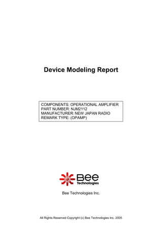
- 1. Device Modeling Report COMPONENTS: OPERATIONAL AMPLIFIER PART NUMBER: NJM2112 MANUFACTURER: NEW JAPAN RADIO REMARK TYPE: (OPAMP) Bee Technologies Inc. All Rights Reserved Copyright (c) Bee Technologies Inc. 2005
- 2. Spice Model U17 + - + - + - + - + - NJM2112 All Rights Reserved Copyright (c) Bee Technologies Inc. 2005
- 3. Output Voltage Swing Simulation result 3.03V 2.00V 0V -2.00V -5.0V -4.0V -3.0V -2.0V V(Vout) V_V1 Evaluation circuit Rload 10k Vout U16 + - + - + - V- V1 V+ + - + - 0Vdc -2.5Vdc 2.5Vdc NJM2112 0 0 Comparison table Output Voltage Swing Data sheet Simulation %Error V+ 2.2 2.2 0 V- 2.2 2.2 0 All Rights Reserved Copyright (c) Bee Technologies Inc. 2005
- 4. Input Offset Voltage Simulation result 4.0V 0V -4.0V -10mV -5mV 0V 5mV 10mV V(Vout) V_Vin Evaluation circuit Rload 10k Vout U11 + - + - + - Vi VOFF = 0 VAMPL = 0 V+ + - + - FREQ = 0 Vin AC = 0 VOFF = 0 V- DC = 0 VAMPL = 0 2.5Vdc FREQ = 0 NJM2112 AC = 0 -2.5Vdc DC = 0 0 0 Comparison table Measurement Simulation Error Vos 1 mV 1.04 mV 4 % All Rights Reserved Copyright (c) Bee Technologies Inc. 2005
- 5. Slew Rate Simulation result 4.0V 0V -4.0V 0s 1.0us 2.0us 3.0us V(Vout) Time Evaluation circuit Rload 10k Vout U16 + - + - + - V1 = 0 Vi V2 = 14 Vin TD = 0 VOFF = 0 TR = 10n V+ V- VAMPL = 0 TF = 10n + - + - FREQ = 0 PW = 5u AC = 0 PER = 500u 2.5Vdc -2.5Vdc DC = 0 V2 NJM2112 -1.04m 0 0 Comparison table Data sheet Simulation %Error Slew Rate(v/us) 3.2 3.201 0.031 All Rights Reserved Copyright (c) Bee Technologies Inc. 2005
- 6. Input current Simulation result 300nA 200nA 100nA 0A 0s 0.5ms 1.0ms I(Vin) Time Evaluation circuit Rload 10k Vout U15 + - + - + - VOFF = -1.04m Vi Vin VOFF = 0 VAMPL = 0 VAMPL = 0 V+ V- + - + - FREQ = 0 FREQ = 0 AC = 0 AC = 0 DC = 0 DC = 0 2.5Vdc -2.5Vdc NJM2112 0 0 Comparison table Data sheet Simulation %Error Ib(nA) 100 98.310 -1.69 All Rights Reserved Copyright (c) Bee Technologies Inc. 2005
- 7. Open Loop Voltage Gain vs. Frequency Simulation result 100 50 0 1.0Hz 100Hz 10KHz 1.0MHz DB(V(Vout)/V(Vin:+)) Frequency Evaluation circuit Vout U17 + - + - + - Vin Vi V+ VOFF = 0 VOFF = 0 + - + - V- VAMPL = 0 VAMPL = 0 FREQ = 0 FREQ = 0 2.5Vdc AC = 1m AC = 0 -2.5Vdc NJM2112 DC = -1.04m DC = 0 0 Comparison table Data sheet Simulation %Error f-0dB(MHz) 9 8.833 -1.855 Av-dc 80 79.672 -0.41 All Rights Reserved Copyright (c) Bee Technologies Inc. 2005
- 8. Common-Mode Rejection Voltage gain Simulation result 2.0V 1.0V 0V -1.0V 0s 1.0s 2.0s 3.0s 4.0s V(Vout) Time Evaluation circuit Vout U15 + - + - -1.04m V2 + - V+ V- + - + - V1 VOFF = 0 2.5Vdc -2.5Vdc VAMPL = 0.5 NJM2112 FREQ = 1 0 Common Mode Reject Ratio=9629.417/2.204 = 4369.06 = 77.94dB Comparison table Data sheet Simulation %Error CMRR(dB) 74 72.80 1.621 All Rights Reserved Copyright (c) Bee Technologies Inc. 2005