VLSI refers to very large scale integration in electronics, involving the integration of millions of transistors on a single chip. The document discusses the history and evolution of integration levels from SSI to VLSI to ULSI. It describes the CMOS fabrication process and design styles used in VLSI. Key phases in chip creation are design, fabrication, testing and packaging. Advanced computer-aided design tools are needed to design complex VLSI circuits. Applications include analog, ASIC and system-on-chip designs. Challenges to VLSI include power dissipation and scaling issues as integration increases. The future of VLSI involves continued device miniaturization and increasing transistor densities on chips.
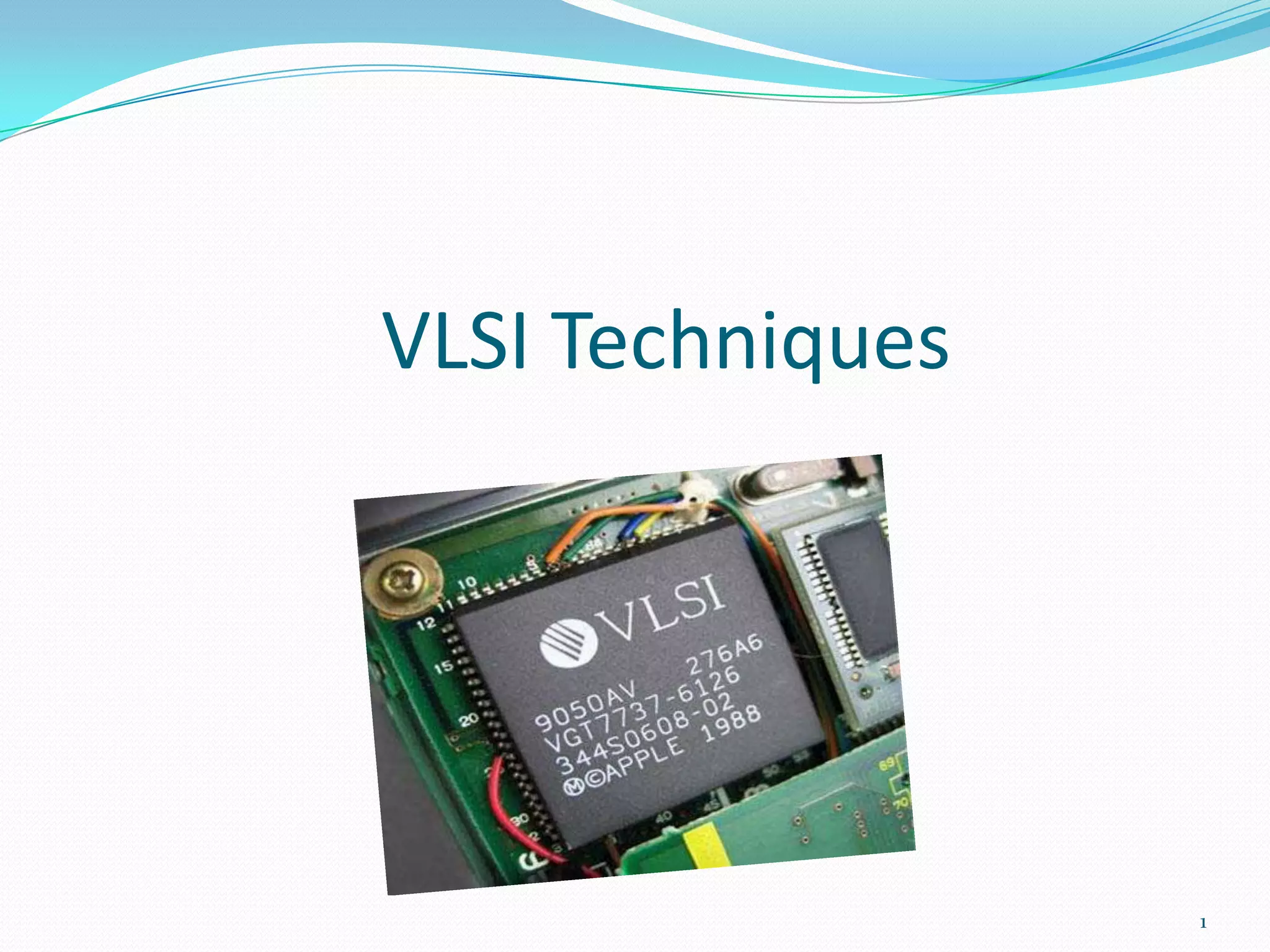
VLSI Design
Whatis VLSI?
“Very Large Scale Integration”
Defines integration level
1980s hold-over from outdated taxonomy for integration levels
Obviously influenced from frequency bands, i.e. HF, VHF, UHF
Sources disagree on what is measured (gates or transistors?)
SSI – Small-Scale Integration (0-102)
MSI – Medium-Scale Integration (102-103)
LSI – Large-Scale Integration (103-105)
VLSI – Very Large-Scale Integration (105-107)
ULSI – Ultra Large-Scale Integration (>=107)
2
3.
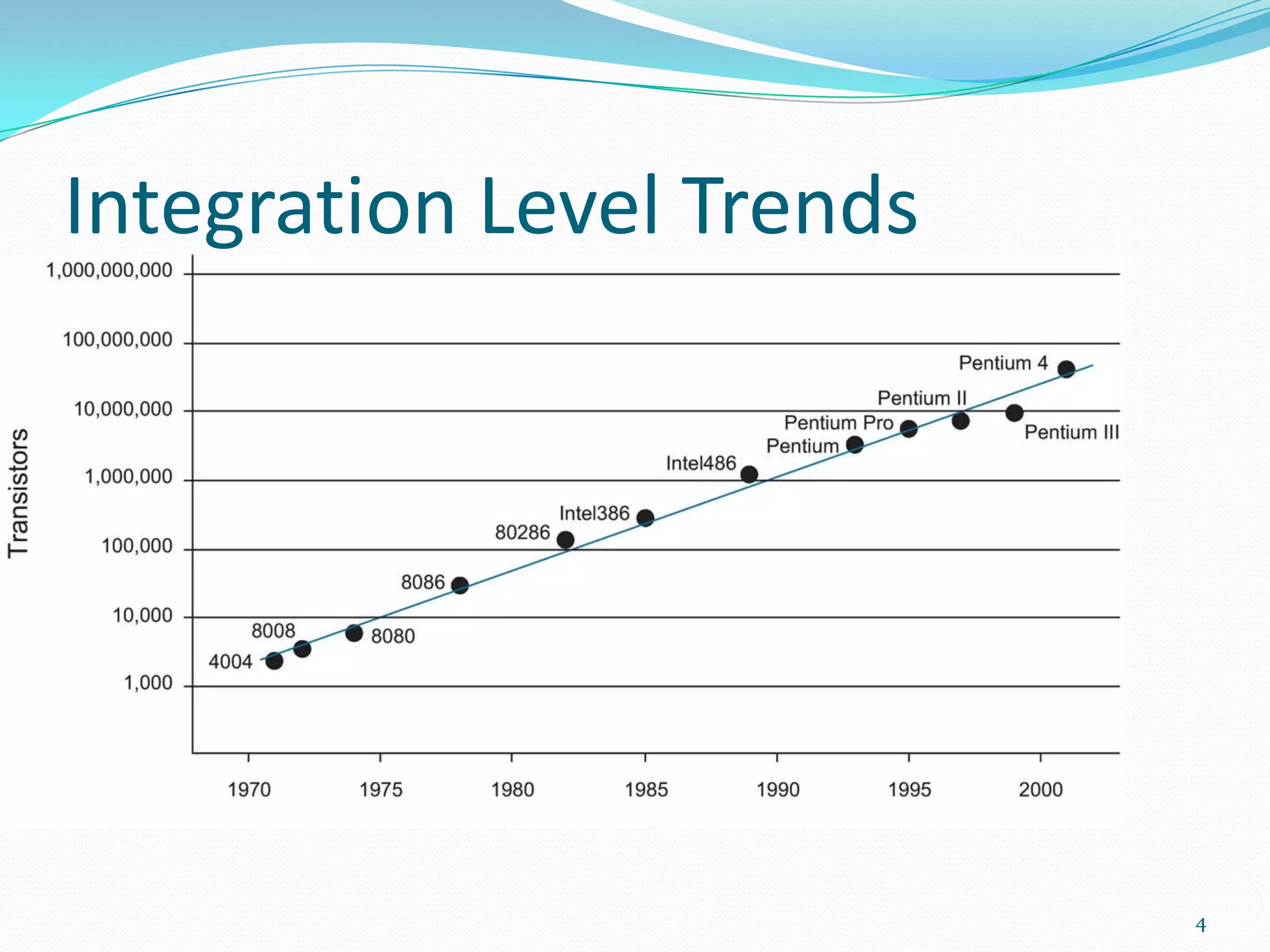
Moore’s Law
In1960 Gordon Moore predicted “the number of
components that can be integrated on a single chip
would increase at such a rapid rate that it will become
twice in every 18 months”.
So by using Moore’s law we get an approximate
integration level trend at any time.
But now moore’s law has reached its physical limit.
3
Integrated Circuits/MEMs
Today,VLSI refers to systems implementation with integrated
circuits
Integrated circuit refers mostly to general manufacturing technique
micro/nano-scale devices on a semiconductor (crystalline) substrate
Formed using chemical/lithography processing
What kind of devices / structures?
transistors (bipolar, MOSFET)
wires (interconnects and passives)
diodes (junction, LEDs, VCSELs, MSM, photoconductor, PiN)
MEMs (piezoelectric integration, accelerometers, gyroscopes,
pressure sensors, micro-mirrors)
For CMOS digital design, we only use MOSFET transistors (used
as switches) and wires
5
6.
Chips
Integrated circuitsconsist of:
A small square or rectangular “die”, < 1mm thick
Small die: 1.5 mm x 1.5 mm => 2.25 mm2
Large die: 15 mm x 15 mm => 225 mm2
Larger die sizes mean:
More logic, memory
Less volume
Less yield
Dies are made from silicon (substrate)
Substrate provides mechanical support and electrical common point
6
7.
CMOS technique ofIC fabrication
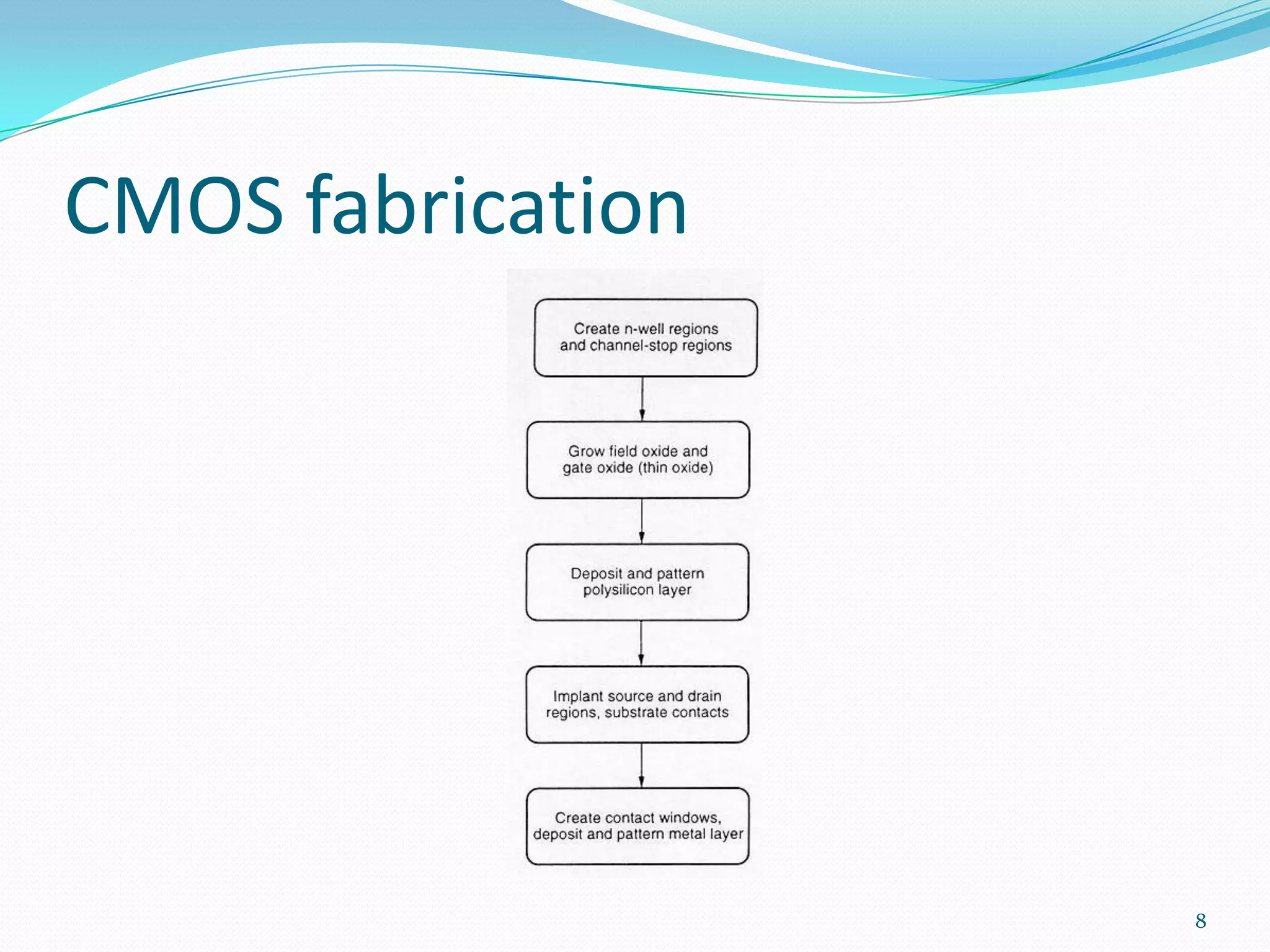
Common metal oxide semiconductor for constructing
FET on wafer chip
N-well technique of fabrication on doped silicon, poly
silicon, metal oxide and silicon oxide layer is
implemented.
On this pattern of various layers Optical lithography
followed by photo resisting and etching is done.
7
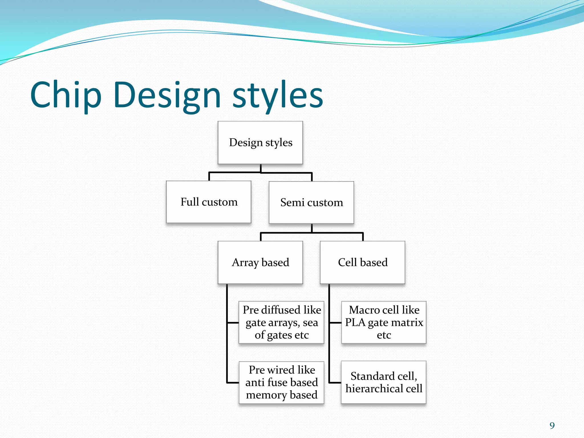
Chip Design styles
Design styles
Full custom Semi custom
Array based Cell based
Pre diffused like Macro cell like
gate arrays, sea PLA gate matrix
of gates etc etc
Pre wired like
Standard cell,
anti fuse based
hierarchical cell
memory based
9
10.
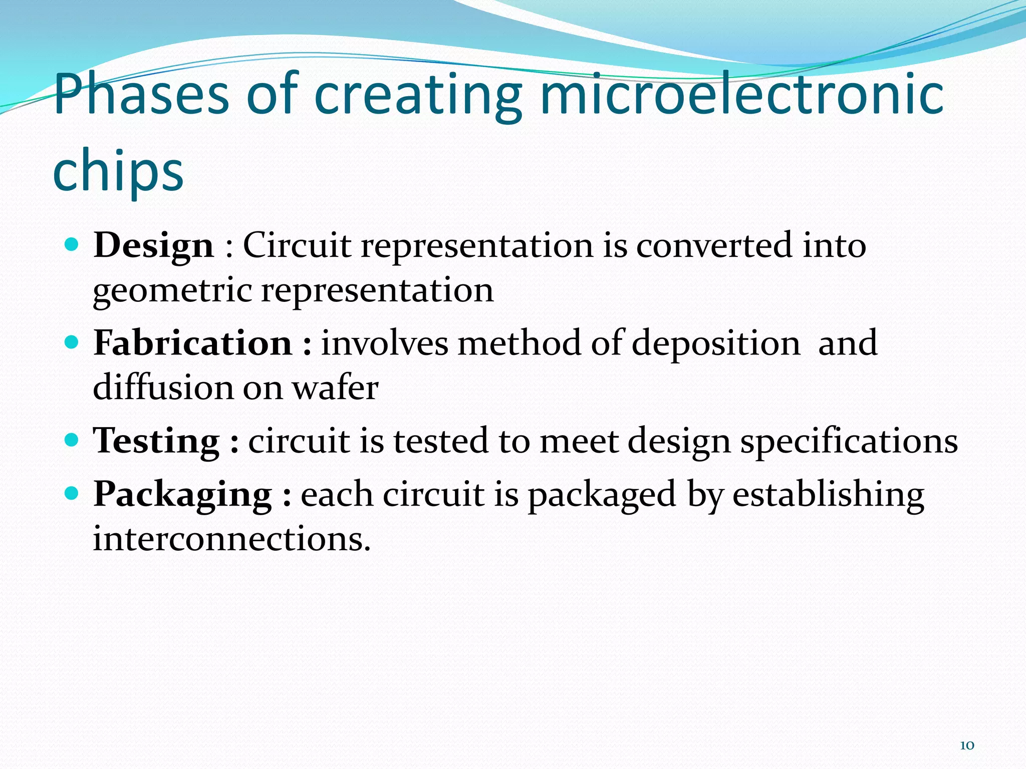
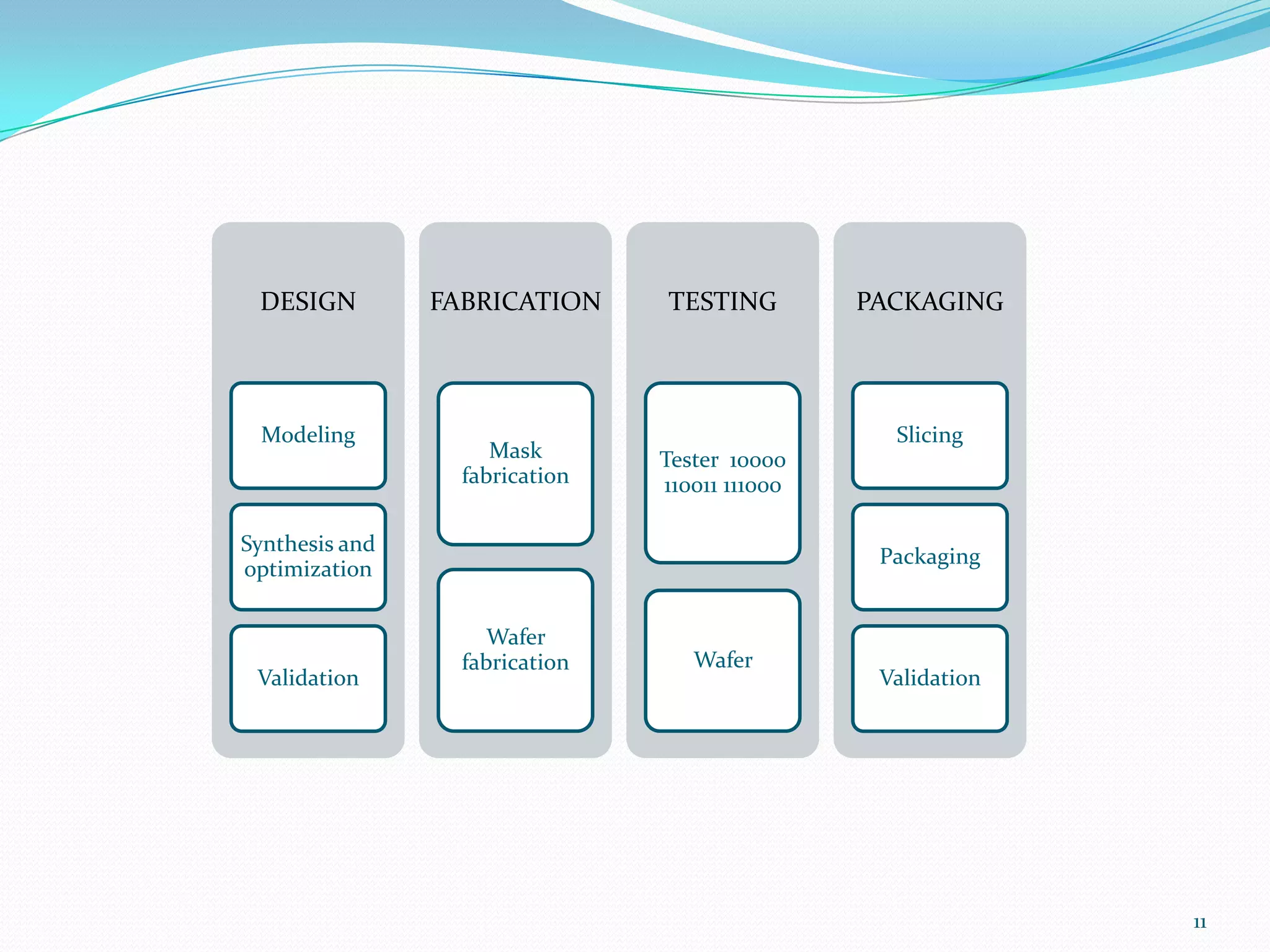
Phases of creatingmicroelectronic
chips
Design : Circuit representation is converted into
geometric representation
Fabrication : involves method of deposition and
diffusion on wafer
Testing : circuit is tested to meet design specifications
Packaging : each circuit is packaged by establishing
interconnections.
10
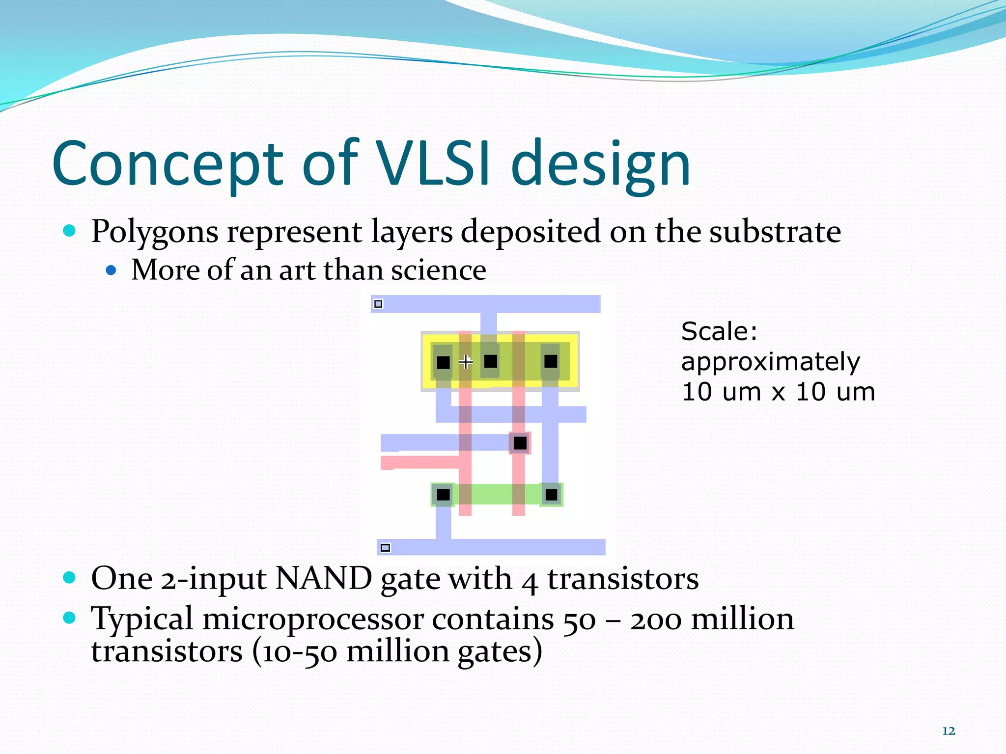
Concept of VLSIdesign
Polygons represent layers deposited on the substrate
More of an art than science
Scale:
approximately
10 um x 10 um
One 2-input NAND gate with 4 transistors
Typical microprocessor contains 50 – 200 million
transistors (10-50 million gates)
12
13.
Need of computerizeddesign tools
Manual layout of complex large scale design is obviously not practical
Design complexity:
Manually drawing layout for a billion transistors would take too long
Even if we could… there are many problems like…
How to verify (test) designs for functionality, speed, power, etc.?
Complexity scales faster than actual design
How to reuse designs?
How to create human-readable designs?
How to speed-up design process?
These problems form a great deal of work
Electronic Design Automation (EDA)
a.k.a. CAD
13
14.
VLSI CAD
Varioussoftware like synopsys , cadence etc. are used
by designers to synthesize highly efficient VLSI chips.
Hardware description for IC is written in Verilog or
VHDL.
It describes the hardware ,interconnection of circuit
blocks and functionality.
VHDL(very high speed IC hardware design language)
is the C of VLSI technology.
14
15.
VLSI applications
Basicallythree areas of application exist today for VLSI
Analog : Small transistor count precision circuits such
as Amplifiers, Data converters, filters, Phase Locked
Loops, Sensors etc.
ASIC: application specific IC a microchip to perform and
execute a particular task like digital signal processing,
image compression etc.
SoC: systems on a chip are highly complex mixed signal
processors like a network chip or a wireless radio chip.
15
16.
Challenges to VLSItechnology
As integration increases VLSI chips somewhat suffer
from the challenges such as
Power dissipation due to increasing components
Noise delays due to capacitive or inductive coupling
Decrease in clock frequency by skin effect on VLSI chip
Improper scaling of wires for increasing components.
16
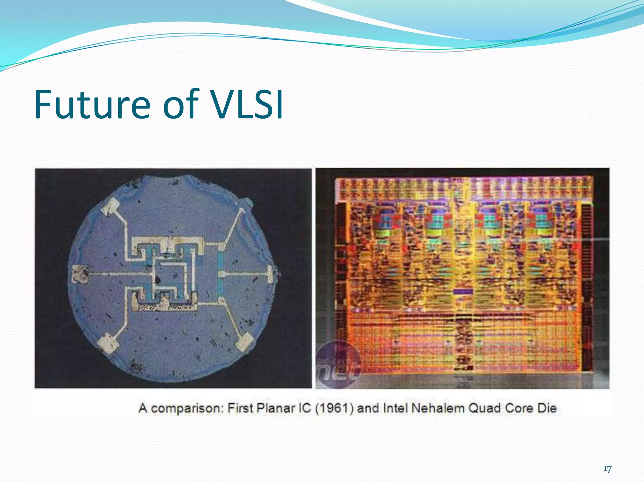
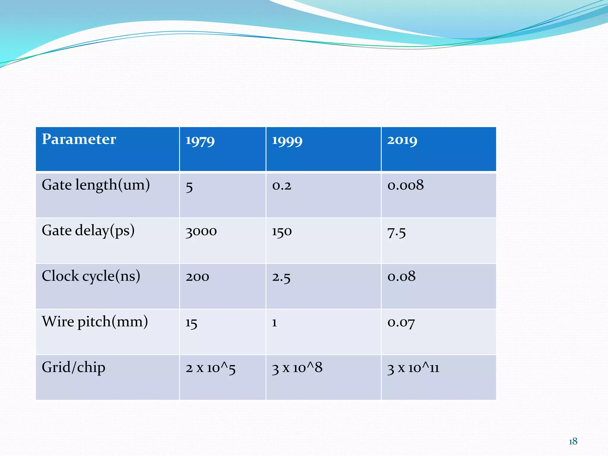
Future of VLSI
Technology is evolving everyday and VLSI is the most
progressing one it is moving to ULSI.
It has been predicted that VLSI will develop more in
the coming decade.
19