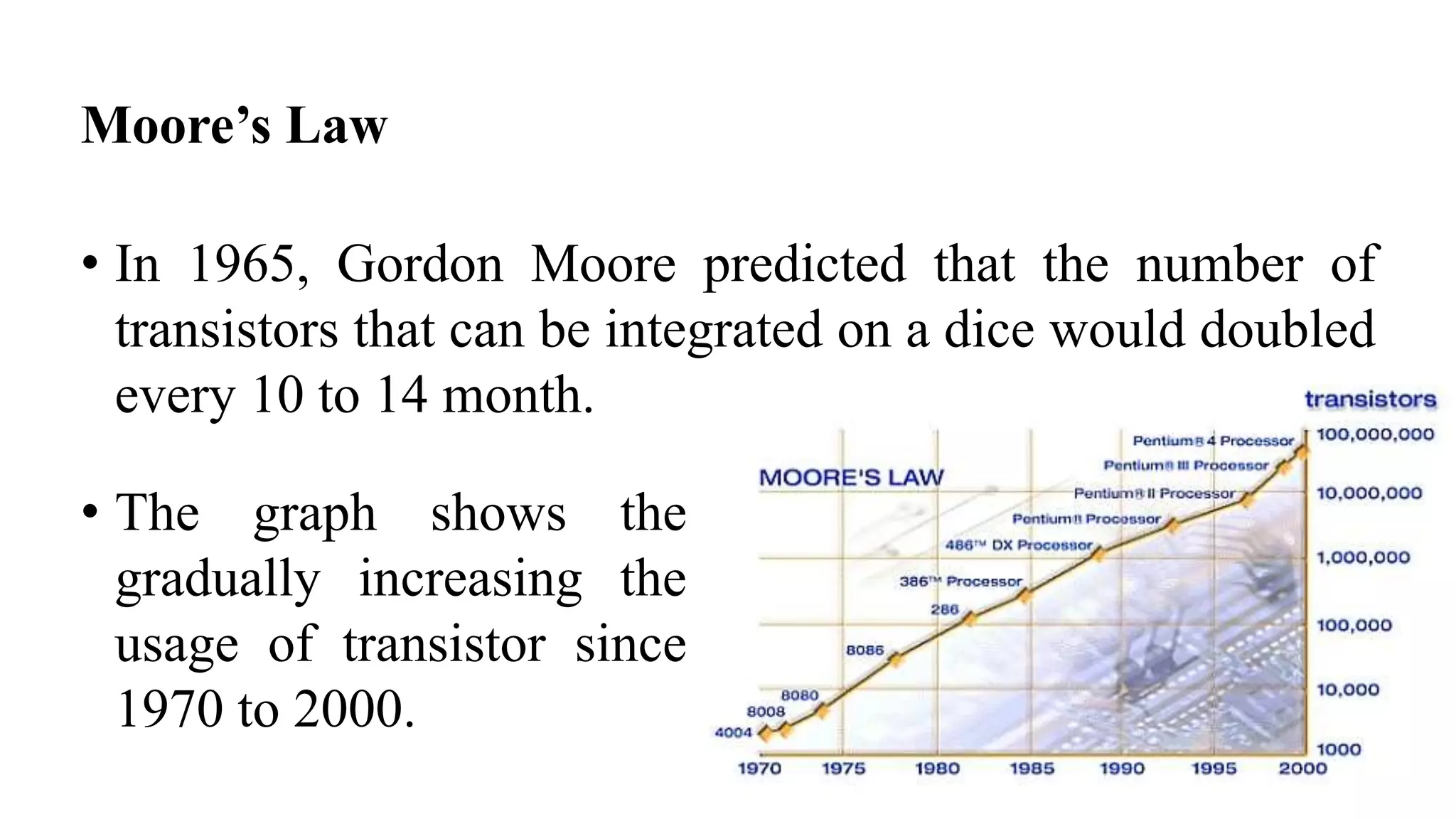
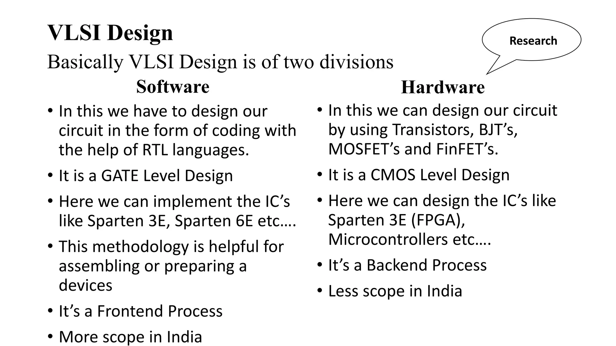
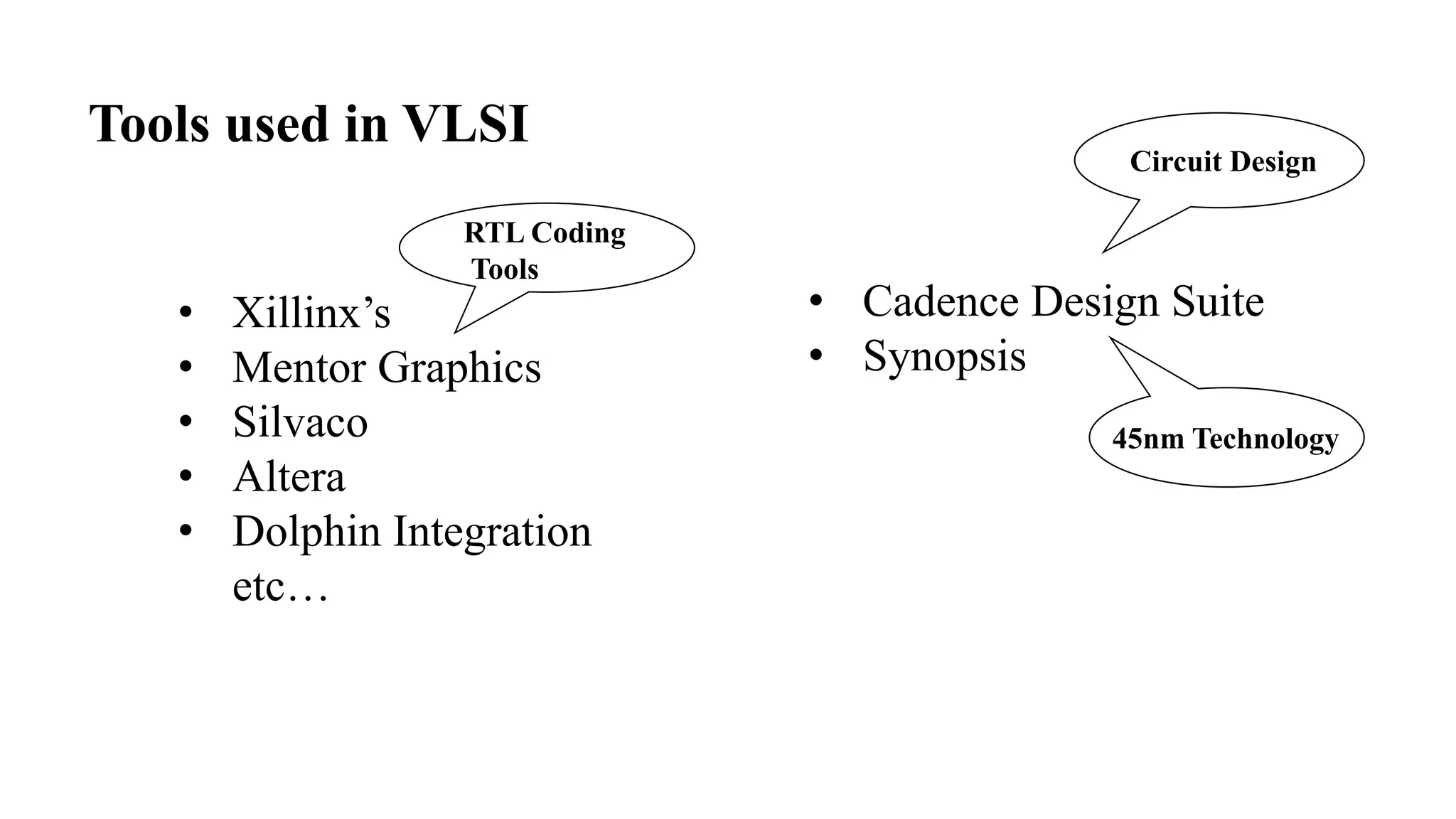
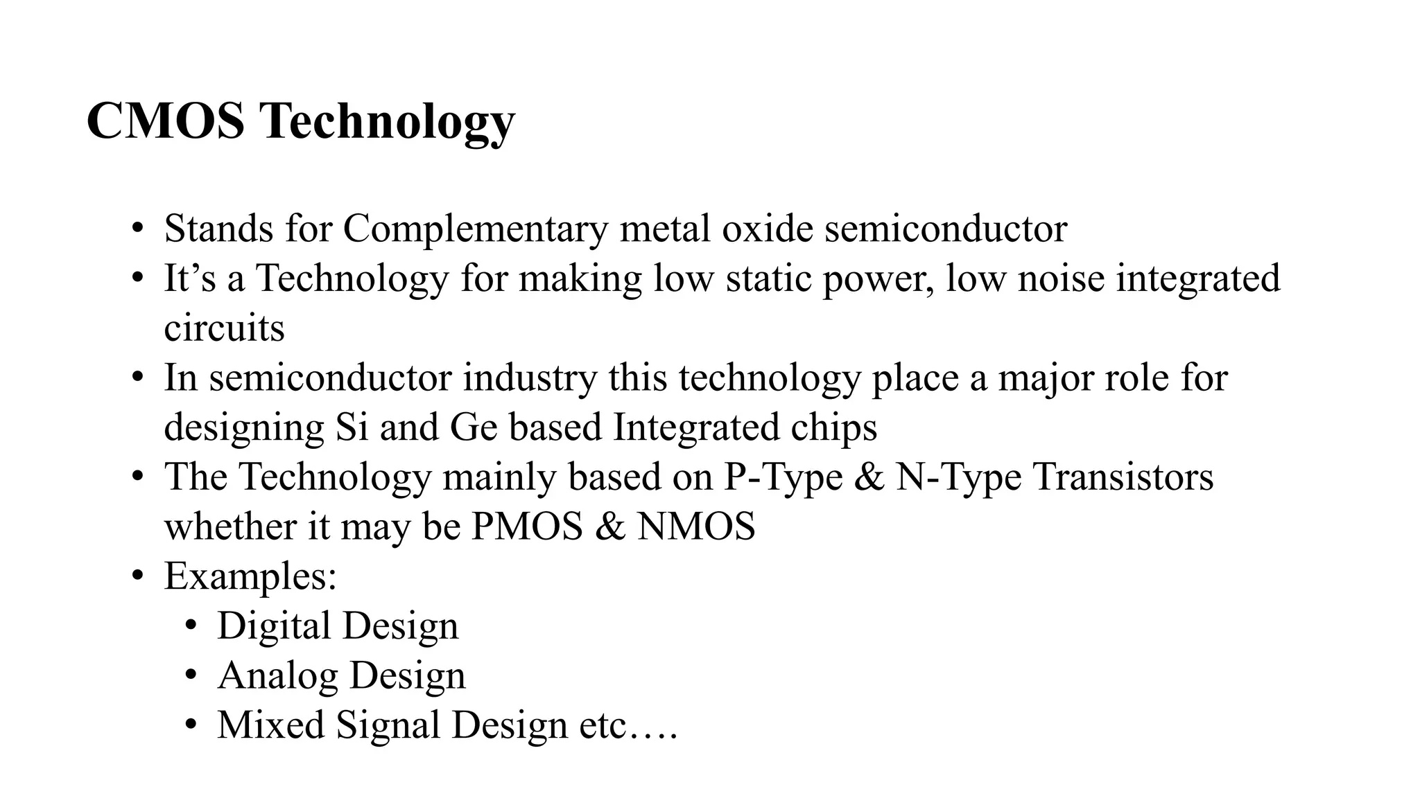
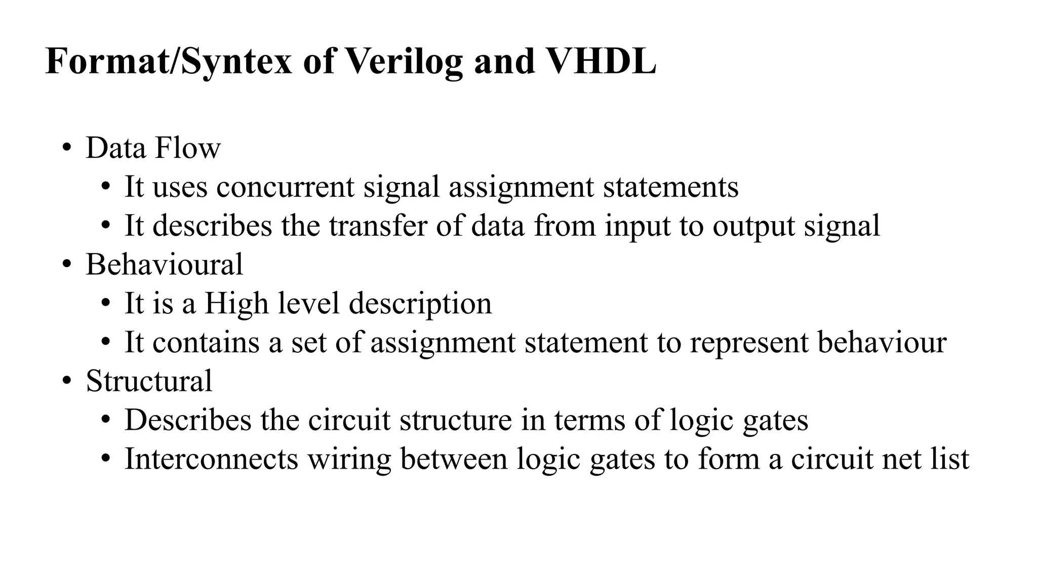
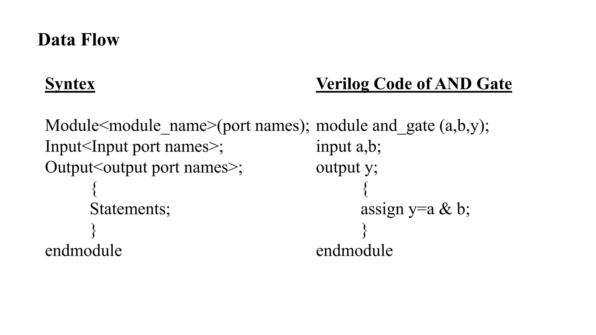
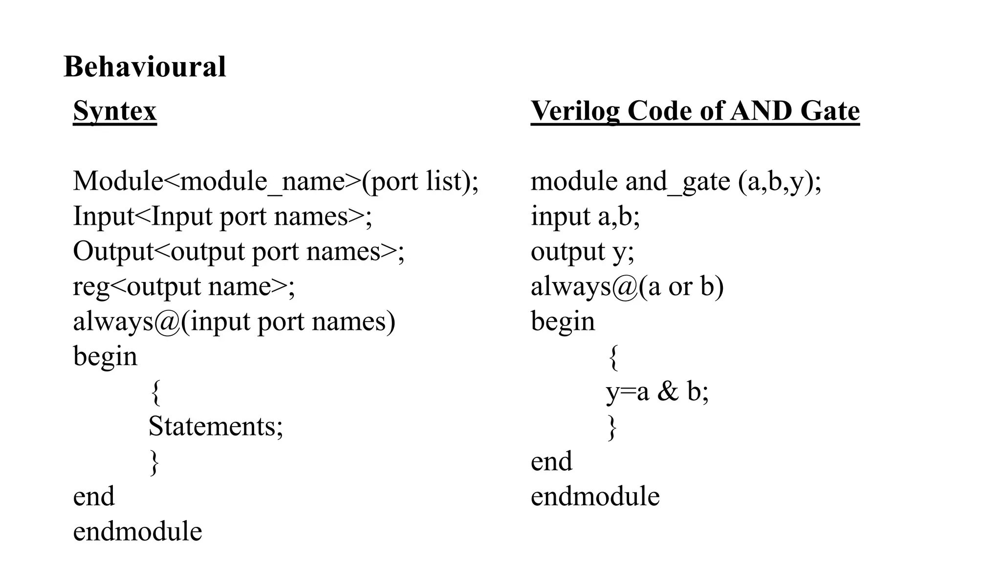
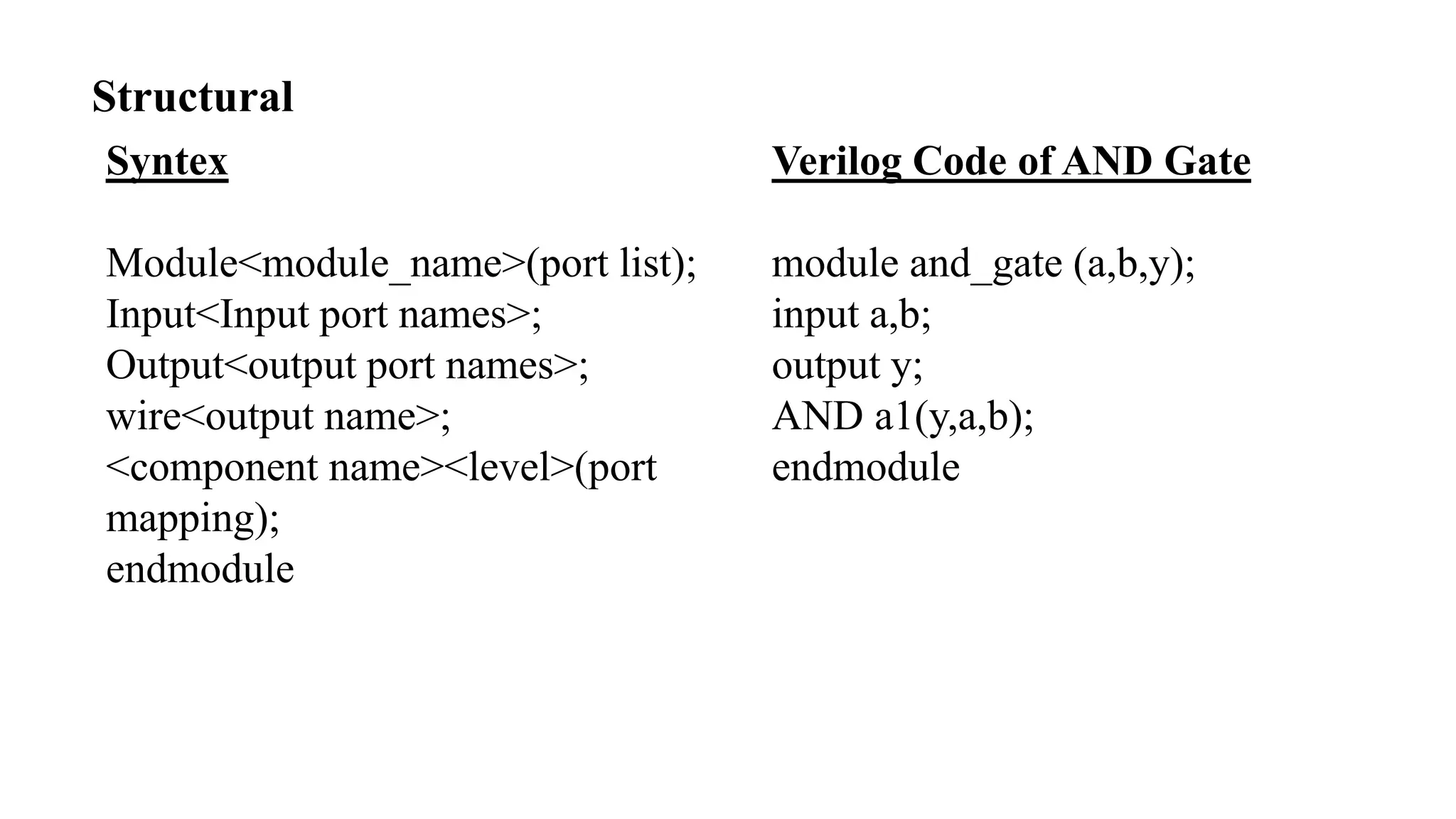
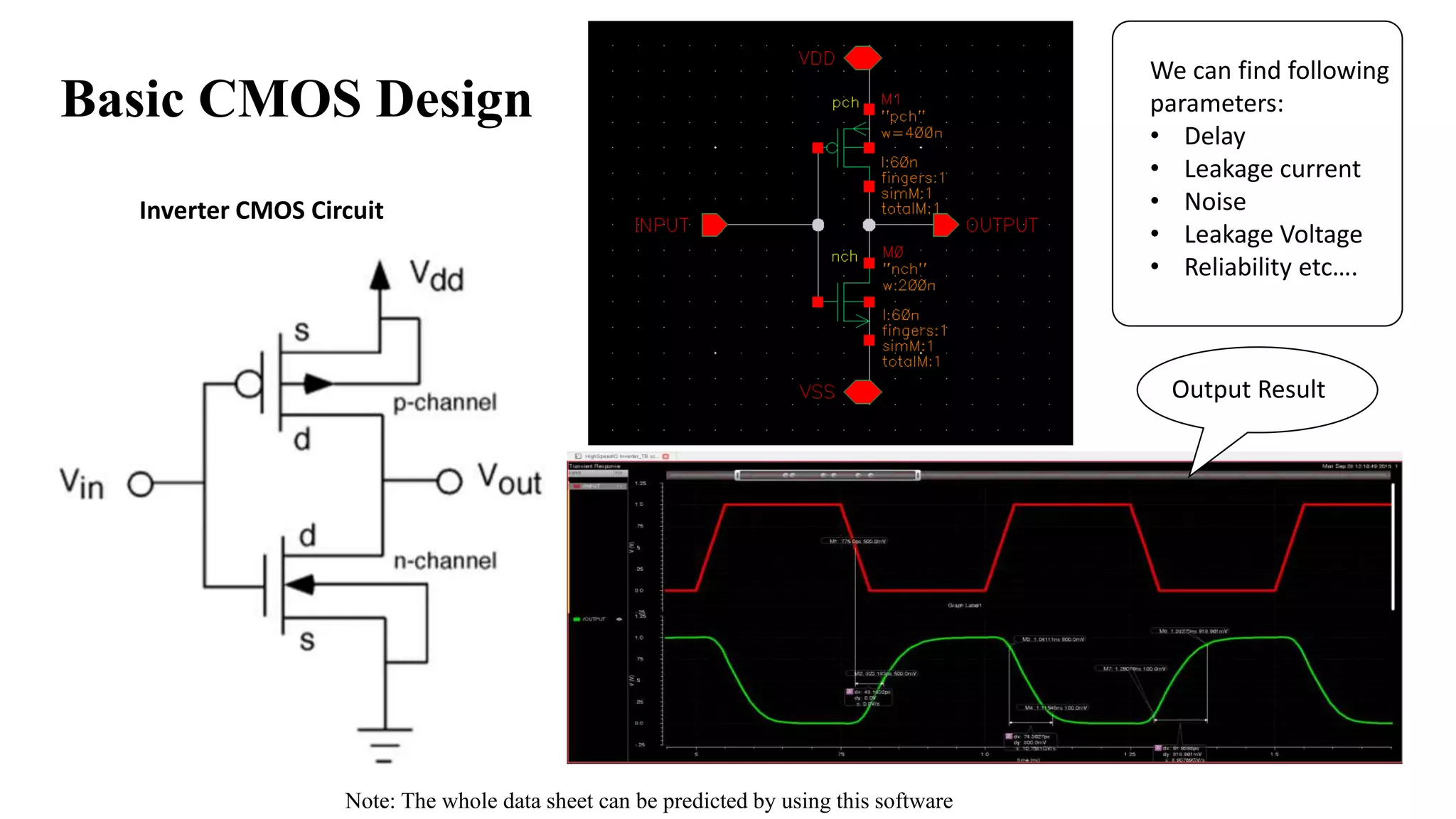
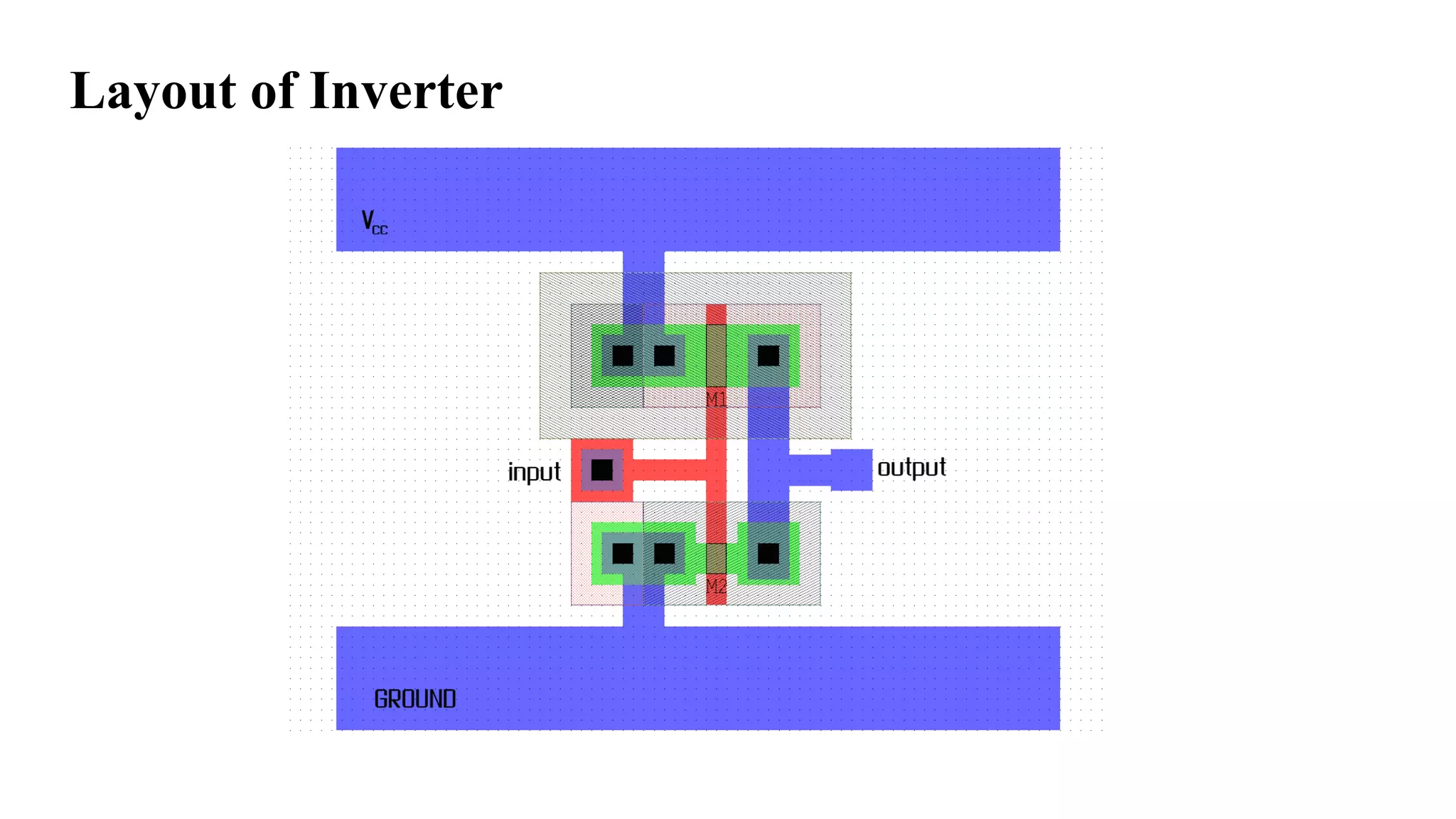
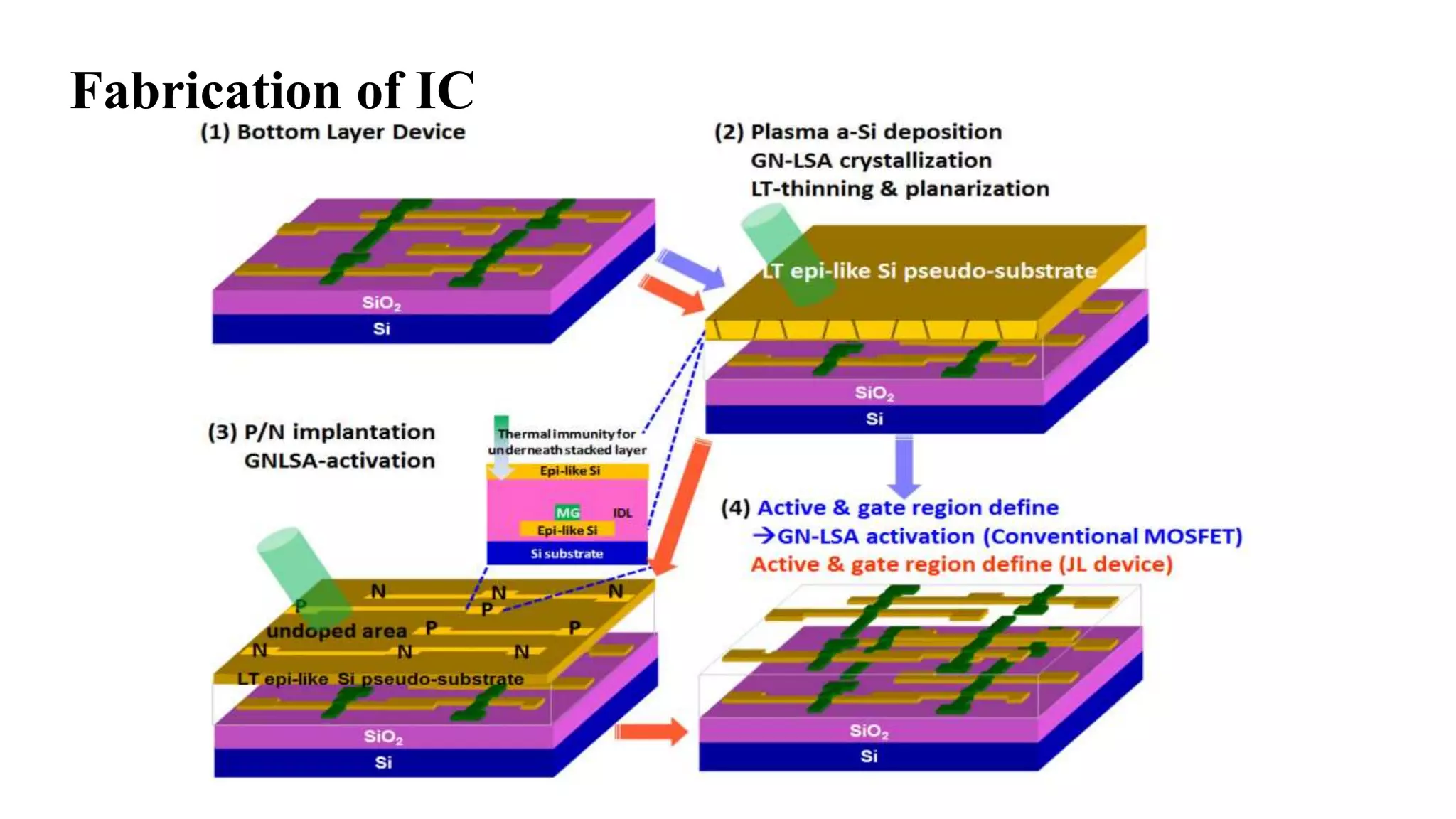
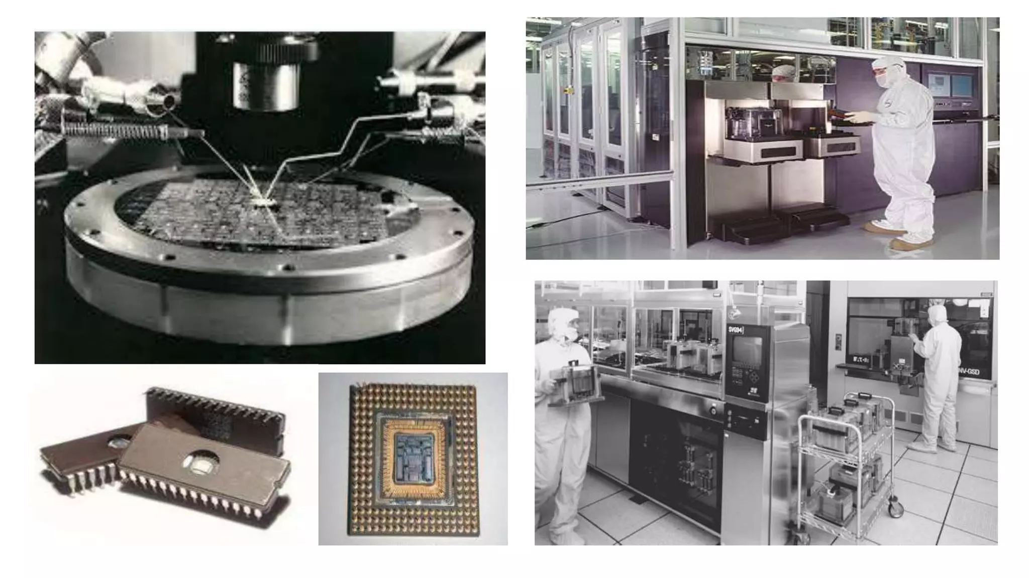
PRESENTATION
ON
VERY LARGE SCALE INTEGRATION
(VLSI) TECHNOLOGY
Presented By:
Seelam Vasavi Sai Viswanada Prabhu Deva Kumar
Electronics & Communication Engineering
ITM University, Gwalior.
Guided By-
Dr. Shyam Akashe
Head of Department
(Electronics and Communication)
ITM University, Gwalior.
• Introduction
• Moore’s Law
• What is VLSI?
• VLSI Design
• Tools used in VLSI
• CMOS Technology
• Basic difference between Verilog and VHDL
• Format/Syntex of Verilog and VHDL
• Basic Verilog Codes
• Basic CMOS Design
• Layout of Inverter
• Fabrication of IC
• Advantages
• Disadvantages
• VLSI Companies in India
• Conclusion
• References
• Biography
Contents
Introduction
• Process of creating IC’s (Integrated Circuits)
by combining thousands of transistor based in
a single chip.
• Design and manufacturing of extremely
small, complex circuits by semiconductor
material.
Moore’s Law
• In 1965, Gordon Moore predicted that the number of
transistors that can be integrated on a dice would doubled
every 10 to 14 month.
• The graph shows the
gradually increasing the
usage of transistor since
1970 to 2000.
What is VLSI?
• VLSI stands for Very Large Scale Integration
• It defines the Integration level
• This VLSI Technology came out after the
implementation of
• SSI- Small Scale Integration
• MSI- Medium Scale Integration
• LSI- Large Scale Integration
• Later new Technology is ULSI (Ultra Large Scale
Integration)
VLSI Design
Software
• In this we have to design our
circuit in the form of coding with
the help of RTL languages.
• It is a GATE Level Design
• Here we can implement the IC’s
like Sparten 3E, Sparten 6E etc….
• This methodology is helpful for
assembling or preparing a
devices
• It’s a Frontend Process
• More scope in India
Hardware
• In this we can design our circuit
by using Transistors, BJT’s,
MOSFET’s and FinFET’s.
• It is a CMOS Level Design
• Here we can design the IC’s like
Sparten 3E (FPGA),
Microcontrollers etc….
• It’s a Backend Process
• Less scope in India
Basically VLSI Design is of two divisions
Research
Tools used in VLSI
• Xillinx’s
• Mentor Graphics
• Silvaco
• Altera
• Dolphin Integration
etc…
• Cadence Design Suite
• Synopsis
RTL Coding
Tools
Circuit Design
45nm Technology
CMOS Technology
• Stands for Complementary metal oxide semiconductor
• It’s a Technology for making low static power, low noise integrated
circuits
• In semiconductor industry this technology place a major role for
designing Si and Ge based Integrated chips
• The Technology mainly based on P-Type & N-Type Transistors
whether it may be PMOS & NMOS
• Examples:
• Digital Design
• Analog Design
• Mixed Signal Design etc….
Basic difference between Verilog and VHDL
Verilog HDL
• Verilog Hardware Description
Language
• Case Sensitive
• Easy to learn
• Based on C
• Not Strongly Typed
VHDL
• Very High Speed Integration
Circuit (VHISIC) Hardware
Description Language
• Not Case Sensitive
• Difficult to learn
• Based on pascal & ada
• Strongly Typed (Because of IEEE
Standards)
Format/Syntex of Verilog and VHDL
• Data Flow
• It uses concurrent signal assignment statements
• It describes the transfer of data from input to output signal
• Behavioural
• It is a High level description
• It contains a set of assignment statement to represent behaviour
• Structural
• Describes the circuit structure in terms of logic gates
• Interconnects wiring between logic gates to form a circuit net list
Data Flow
Verilog Code of AND Gate
module and_gate (a,b,y);
input a,b;
output y;
{
assign y=a & b;
}
endmodule
Syntex
Module<module_name>(port names);
Input<Input port names>;
Output<output port names>;
{
Statements;
}
endmodule
Behavioural
Verilog Code of AND Gate
module and_gate (a,b,y);
input a,b;
output y;
always@(a or b)
begin
{
y=a & b;
}
end
endmodule
Syntex
Module<module_name>(port list);
Input<Input port names>;
Output<output port names>;
reg<output name>;
always@(input port names)
begin
{
Statements;
}
end
endmodule
Structural
Verilog Code of AND Gate
module and_gate (a,b,y);
input a,b;
output y;
AND a1(y,a,b);
endmodule
Syntex
Module<module_name>(port list);
Input<Input port names>;
Output<output port names>;
wire<output name>;
<component name><level>(port
mapping);
endmodule
Basic CMOS Design
Inverter CMOS Circuit
Output Result
We can find following
parameters:
• Delay
• Leakage current
• Noise
• Leakage Voltage
• Reliability etc….
Note: The whole data sheet can be predicted by using this software
Layout of Inverter
Fabrication of IC
Advantages
• Compactness
• Mobility
• Reliability
• Less Power Consumption
• Large Market Background
• Effective use in Real life, Space like Computers,
Mobile Phones, Communication etc…
Disadvantages
• More expensive for designing basic devices.
• No Advancement in Fabrication in India.
• Lack of fabrication training institutes, so
effects on production in India.
VLSI Companies in India
Conclusion
• Learned the applications and scope of VLSI.
• Learned about the applications of VLSI design
software's and programming languages.
• Learned about CMOS technology and Fabrication
process.
• Knew that there is tremendous scope and growth for
those who choose VLSI design as a career.
References
1. VLSI Design at Cambridge Semiconductors (P) LTD By Bhagvan
Lal Teli.
2. VLSI Industrial training at MSME Tool Room Kolkata By Gokul
Buro et. Al.
3. Basics of Very Large Scale Integration (VLSI) By Agwaral Avanish
et. Al.
4. Introduction to VLSI circuits and systems by Soma. O.
Muhammad.
5. VLSI Technology in Microprocessers By Jabez Winston C.
Biography
and his area of interest are LED Fabrication and Designing, Embedded Systems,
IoT (Internet of Things), Low Power VLSI Design, Modeling, CMOS based
memory design, Circuits for future VLSI Technology, Digital Design & FPGA
Implementation. He worked as an Intern in Fuzinix Infotech Pvt. Ltd. and SION
Semiconductors Pvt. Ltd. Seelam Vasavi Sai Viswanada Prabhu Deva Kumar is
authored few research papers in peer reviewed international journals and
magazines. He is an Editorial Member in International Journal of Information
Technology and Computer Science (IJOIT).
Seelam Vasavi Sai Viswanada Prabhu Deva Kumar born at “Chintalapudi”
a city in Andhra Pradesh, India on 15th June 1996. He is pursuing B.Tech
in Electronics & Communication Engineering from Institute of
Technology & Management University (ITM U), Gwalior in 2014-2018
Thank You

VERY LARGE SCALE INTEGRATION (VLSI) TECHNOLOGY

  • 1.
    PRESENTATION ON VERY LARGE SCALEINTEGRATION (VLSI) TECHNOLOGY Presented By: Seelam Vasavi Sai Viswanada Prabhu Deva Kumar Electronics & Communication Engineering ITM University, Gwalior. Guided By- Dr. Shyam Akashe Head of Department (Electronics and Communication) ITM University, Gwalior.
  • 2.
    • Introduction • Moore’sLaw • What is VLSI? • VLSI Design • Tools used in VLSI • CMOS Technology • Basic difference between Verilog and VHDL • Format/Syntex of Verilog and VHDL • Basic Verilog Codes • Basic CMOS Design • Layout of Inverter • Fabrication of IC • Advantages • Disadvantages • VLSI Companies in India • Conclusion • References • Biography Contents
  • 3.
    Introduction • Process ofcreating IC’s (Integrated Circuits) by combining thousands of transistor based in a single chip. • Design and manufacturing of extremely small, complex circuits by semiconductor material.
  • 4.
    Moore’s Law • In1965, Gordon Moore predicted that the number of transistors that can be integrated on a dice would doubled every 10 to 14 month. • The graph shows the gradually increasing the usage of transistor since 1970 to 2000.
  • 5.
    What is VLSI? •VLSI stands for Very Large Scale Integration • It defines the Integration level • This VLSI Technology came out after the implementation of • SSI- Small Scale Integration • MSI- Medium Scale Integration • LSI- Large Scale Integration • Later new Technology is ULSI (Ultra Large Scale Integration)
  • 6.
    VLSI Design Software • Inthis we have to design our circuit in the form of coding with the help of RTL languages. • It is a GATE Level Design • Here we can implement the IC’s like Sparten 3E, Sparten 6E etc…. • This methodology is helpful for assembling or preparing a devices • It’s a Frontend Process • More scope in India Hardware • In this we can design our circuit by using Transistors, BJT’s, MOSFET’s and FinFET’s. • It is a CMOS Level Design • Here we can design the IC’s like Sparten 3E (FPGA), Microcontrollers etc…. • It’s a Backend Process • Less scope in India Basically VLSI Design is of two divisions Research
  • 7.
    Tools used inVLSI • Xillinx’s • Mentor Graphics • Silvaco • Altera • Dolphin Integration etc… • Cadence Design Suite • Synopsis RTL Coding Tools Circuit Design 45nm Technology
  • 8.
    CMOS Technology • Standsfor Complementary metal oxide semiconductor • It’s a Technology for making low static power, low noise integrated circuits • In semiconductor industry this technology place a major role for designing Si and Ge based Integrated chips • The Technology mainly based on P-Type & N-Type Transistors whether it may be PMOS & NMOS • Examples: • Digital Design • Analog Design • Mixed Signal Design etc….
  • 9.
    Basic difference betweenVerilog and VHDL Verilog HDL • Verilog Hardware Description Language • Case Sensitive • Easy to learn • Based on C • Not Strongly Typed VHDL • Very High Speed Integration Circuit (VHISIC) Hardware Description Language • Not Case Sensitive • Difficult to learn • Based on pascal & ada • Strongly Typed (Because of IEEE Standards)
  • 10.
    Format/Syntex of Verilogand VHDL • Data Flow • It uses concurrent signal assignment statements • It describes the transfer of data from input to output signal • Behavioural • It is a High level description • It contains a set of assignment statement to represent behaviour • Structural • Describes the circuit structure in terms of logic gates • Interconnects wiring between logic gates to form a circuit net list
  • 11.
    Data Flow Verilog Codeof AND Gate module and_gate (a,b,y); input a,b; output y; { assign y=a & b; } endmodule Syntex Module<module_name>(port names); Input<Input port names>; Output<output port names>; { Statements; } endmodule
  • 12.
    Behavioural Verilog Code ofAND Gate module and_gate (a,b,y); input a,b; output y; always@(a or b) begin { y=a & b; } end endmodule Syntex Module<module_name>(port list); Input<Input port names>; Output<output port names>; reg<output name>; always@(input port names) begin { Statements; } end endmodule
  • 13.
    Structural Verilog Code ofAND Gate module and_gate (a,b,y); input a,b; output y; AND a1(y,a,b); endmodule Syntex Module<module_name>(port list); Input<Input port names>; Output<output port names>; wire<output name>; <component name><level>(port mapping); endmodule
  • 14.
    Basic CMOS Design InverterCMOS Circuit Output Result We can find following parameters: • Delay • Leakage current • Noise • Leakage Voltage • Reliability etc…. Note: The whole data sheet can be predicted by using this software
  • 15.
  • 16.
  • 18.
    Advantages • Compactness • Mobility •Reliability • Less Power Consumption • Large Market Background • Effective use in Real life, Space like Computers, Mobile Phones, Communication etc…
  • 19.
    Disadvantages • More expensivefor designing basic devices. • No Advancement in Fabrication in India. • Lack of fabrication training institutes, so effects on production in India.
  • 20.
  • 21.
    Conclusion • Learned theapplications and scope of VLSI. • Learned about the applications of VLSI design software's and programming languages. • Learned about CMOS technology and Fabrication process. • Knew that there is tremendous scope and growth for those who choose VLSI design as a career.
  • 22.
    References 1. VLSI Designat Cambridge Semiconductors (P) LTD By Bhagvan Lal Teli. 2. VLSI Industrial training at MSME Tool Room Kolkata By Gokul Buro et. Al. 3. Basics of Very Large Scale Integration (VLSI) By Agwaral Avanish et. Al. 4. Introduction to VLSI circuits and systems by Soma. O. Muhammad. 5. VLSI Technology in Microprocessers By Jabez Winston C.
  • 23.
    Biography and his areaof interest are LED Fabrication and Designing, Embedded Systems, IoT (Internet of Things), Low Power VLSI Design, Modeling, CMOS based memory design, Circuits for future VLSI Technology, Digital Design & FPGA Implementation. He worked as an Intern in Fuzinix Infotech Pvt. Ltd. and SION Semiconductors Pvt. Ltd. Seelam Vasavi Sai Viswanada Prabhu Deva Kumar is authored few research papers in peer reviewed international journals and magazines. He is an Editorial Member in International Journal of Information Technology and Computer Science (IJOIT). Seelam Vasavi Sai Viswanada Prabhu Deva Kumar born at “Chintalapudi” a city in Andhra Pradesh, India on 15th June 1996. He is pursuing B.Tech in Electronics & Communication Engineering from Institute of Technology & Management University (ITM U), Gwalior in 2014-2018
  • 24.