Downloaded 1,229 times


![Input Output Definition
Once the module is defined at the start the inputs and
outputs are to be defined explicitly. e.g.
input a , b //means there are 2 inputs of one bit
each
If input or output is more than 1 bit i.e. two or more bits,
then the definition will be:
input [3:0] A, B; //4 bit inputs A3-A0 and B3-B0
output [3:0] C;](https://image.slidesharecdn.com/veriloghdl-130130165613-phpapp02/75/Verilog-hdl-13-2048.jpg)

![TOP LEVEL MODULE
//Define a 4 bit 4 adder
module toplevel_fa(sum,c_out,a,b,c_in);
//I/O port declaration
output [3:0] sum;
output c_out;
input [3:0] a, b;
input c_in;
//internal nets
wire c1,c2,c3;
//Instantiate four 1-bit full adder
fulladder fa0(sum[0],c1,a[0],b[0],c_in);
fulladder fa1(sum[1],c2,a[1],b[1],c1);
fulladder fa2(sum[2],c3,a[2],b[2],c2);
fulladder fa3(sum[3],c_out,a[3],b[3],c3);
endmodule](https://image.slidesharecdn.com/veriloghdl-130130165613-phpapp02/75/Verilog-hdl-27-2048.jpg)
![Test Bench (stimulus)
//define stimulus toplevel module
module stimulus;
reg [3:0]a,b; //set up variables
reg c_in;
wire [3:0] sum;
wire c_out;
//Instantiate the toplevelmodule(ripple carry adder) call it tl
toplevel_fa tl(sum,c_out,a,b,c_in);](https://image.slidesharecdn.com/veriloghdl-130130165613-phpapp02/75/Verilog-hdl-28-2048.jpg)

Hardware description languages (HDLs) allow designers to describe digital systems at different levels of abstraction in a textual format. The two most commonly used HDLs are Verilog and VHDL. Verilog is commonly used in the US, while VHDL is more popular in Europe. HDLs enable simulation of designs before fabrication to verify functionality. Digital designs can be modeled at the gate level, data flow level, or behavioral level in Verilog. Verilog code consists of a design module and test bench module to stimulate inputs and observe outputs.
HDL (Hardware Description Language) models digital systems, allowing design and simulation before hardware fabrication. Essential in VLSI for verifying complex designs.
Verilog is popular in US, used for digital logic chip design. VHDL is favored in Europe, often for FPGA design.
Common simulators for Verilog include Xilinx, Veriwell, and Model Sim. Veriwell is beginner-friendly.
Verilog has four abstraction levels: Behavioral, Data flow, Gate level, and Switch level, with a focus on Gate, Data flow, and Behavioral modeling.
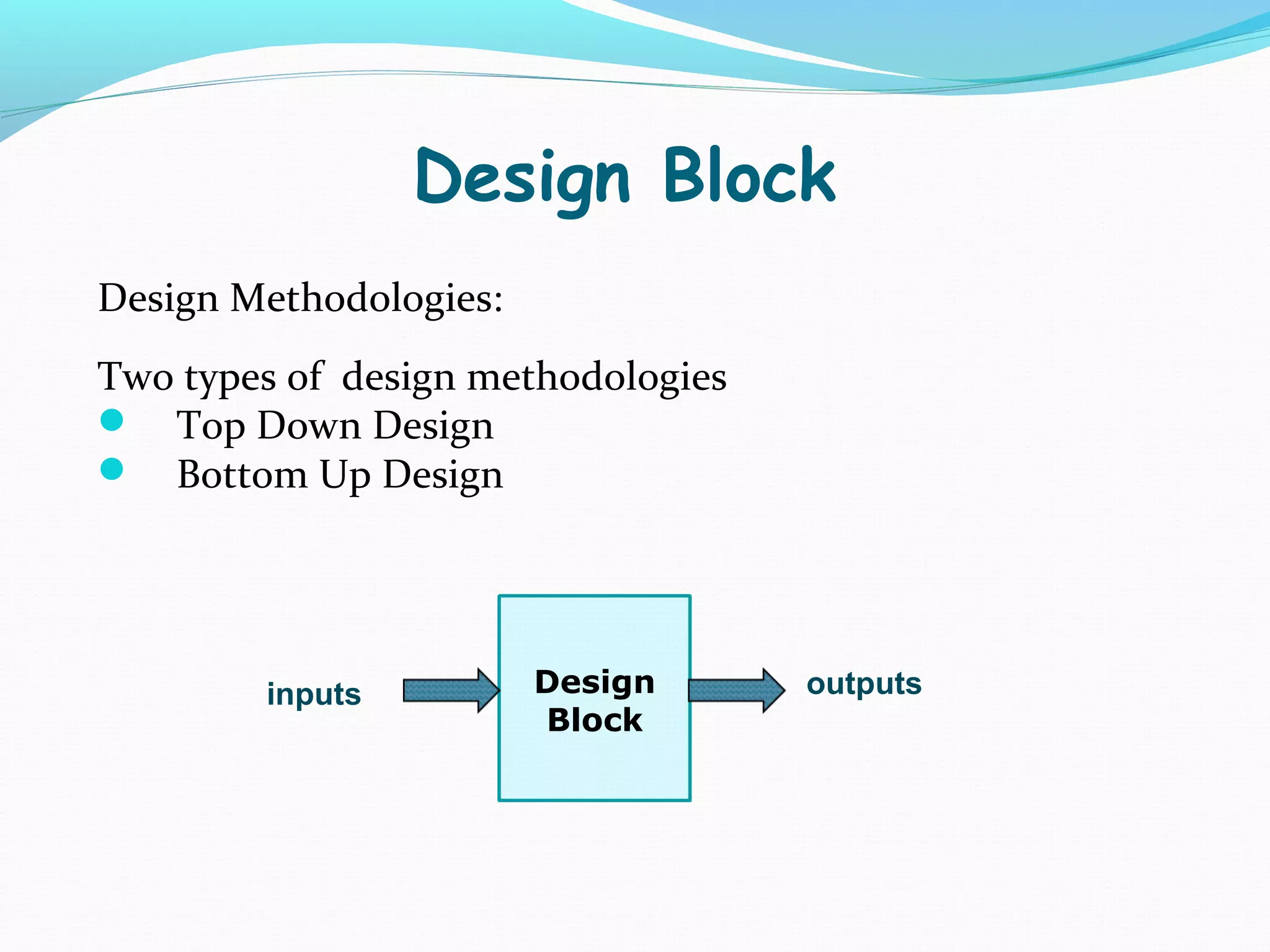
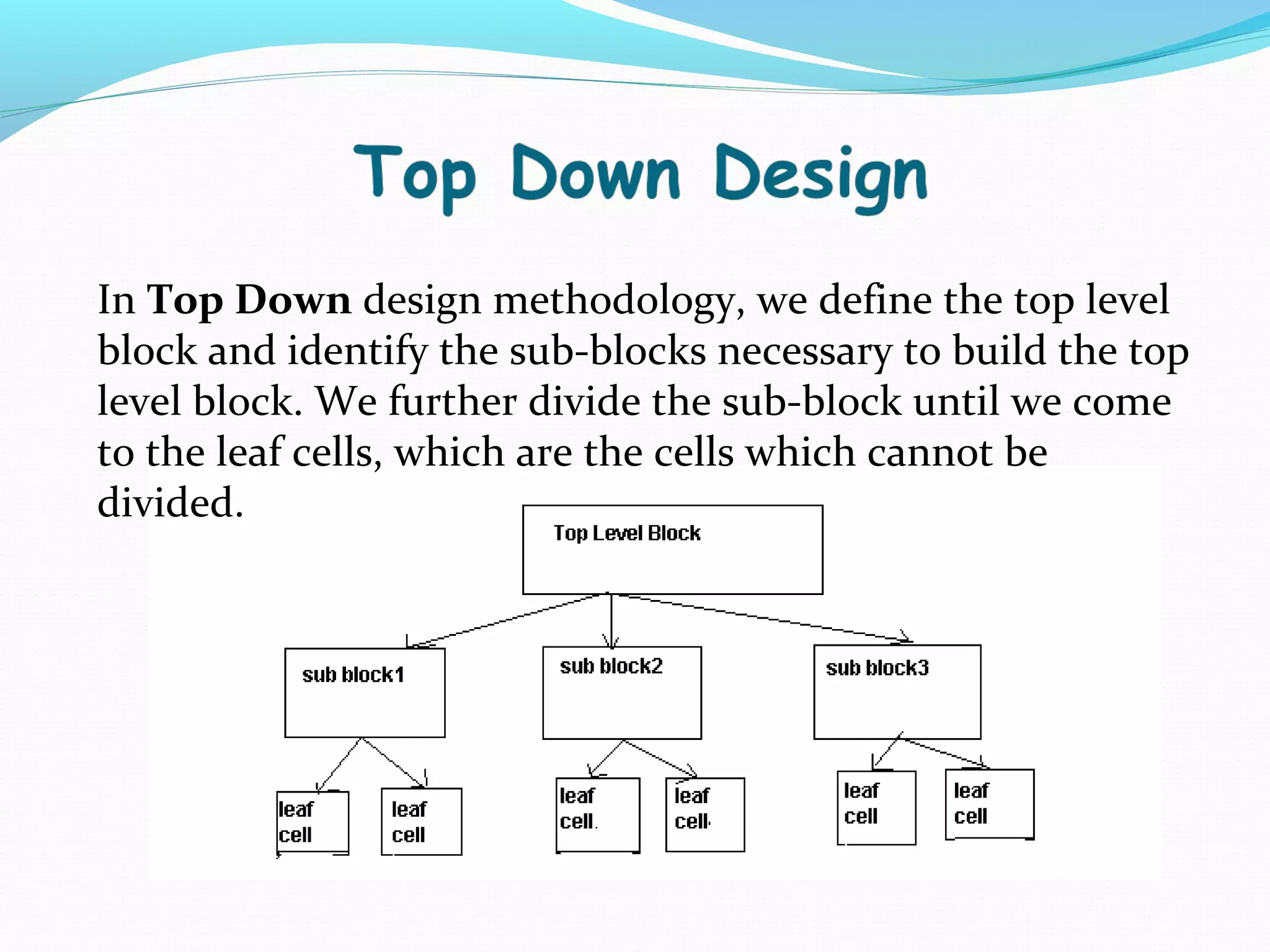
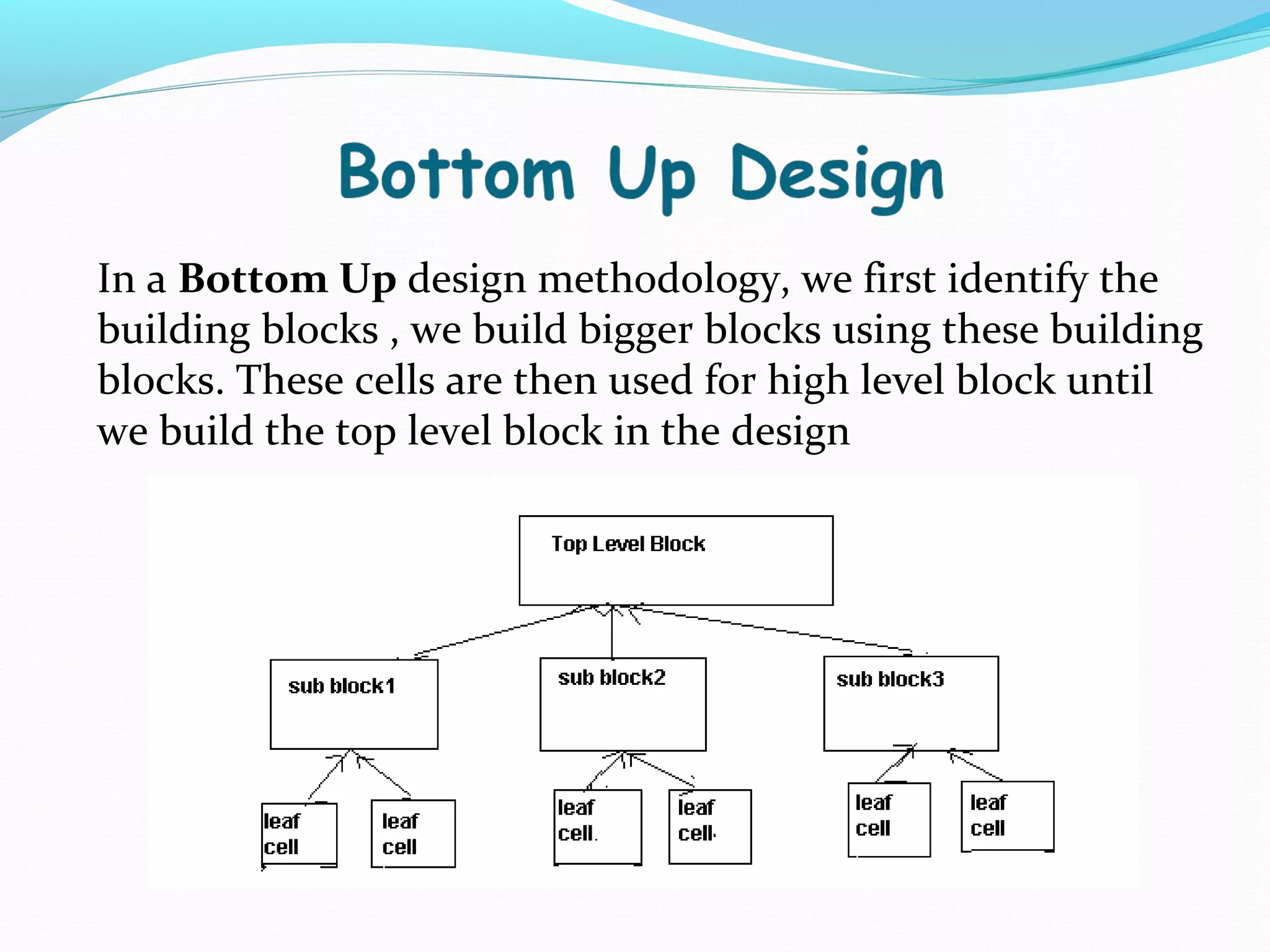
Verilog programs contain a Design Block (Module) and Testing Block (Stimulus). Two methodologies: Top Down and Bottom Up Design.
Top Down design starts with the main block and breaks it down into sub-blocks. Bottom Up design builds higher blocks from identified building blocks.
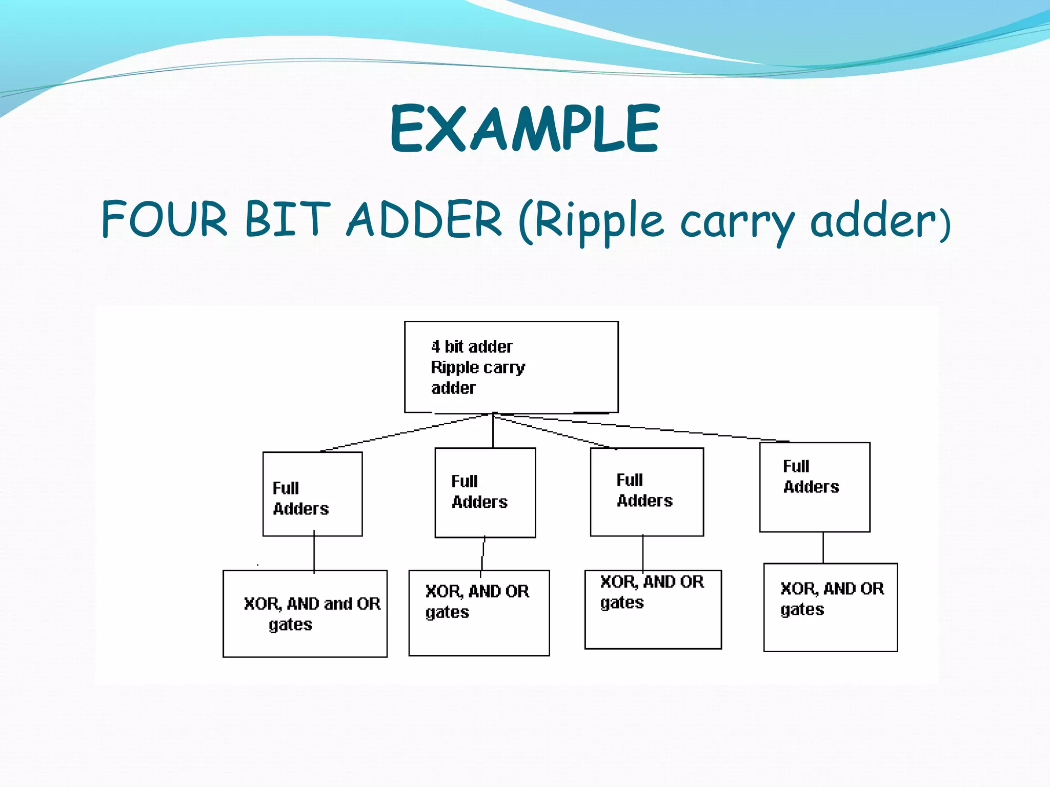
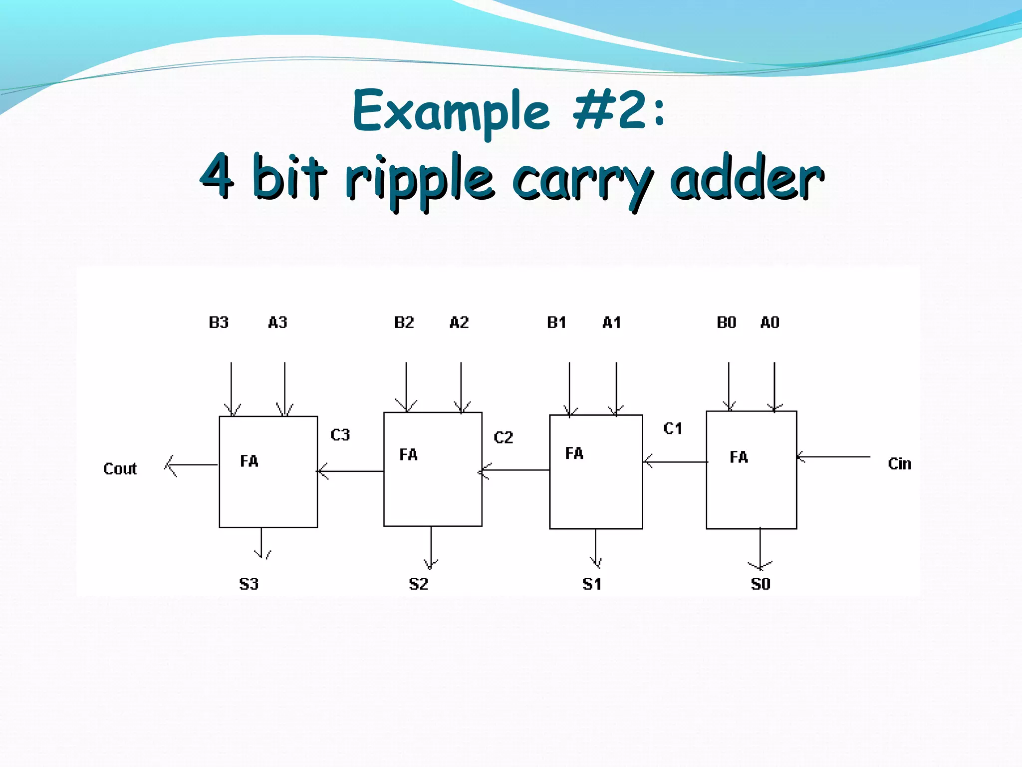
Illustrates a 4-bit adder (Ripple Carry Adder), emphasizing structural design in Verilog.
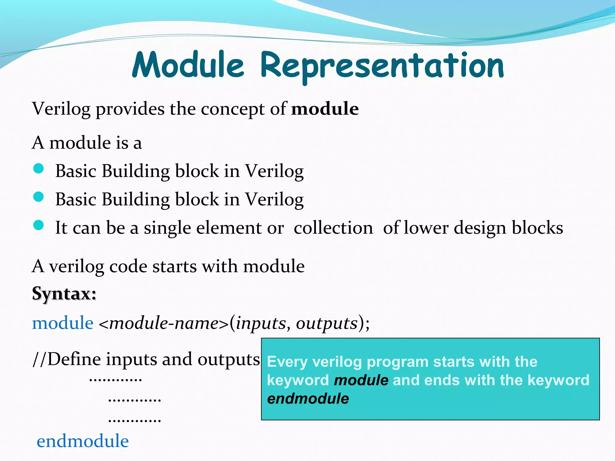
Modules are the basic building blocks in Verilog. Inputs and outputs are defined explicitly. Syntax outlined for module creation.
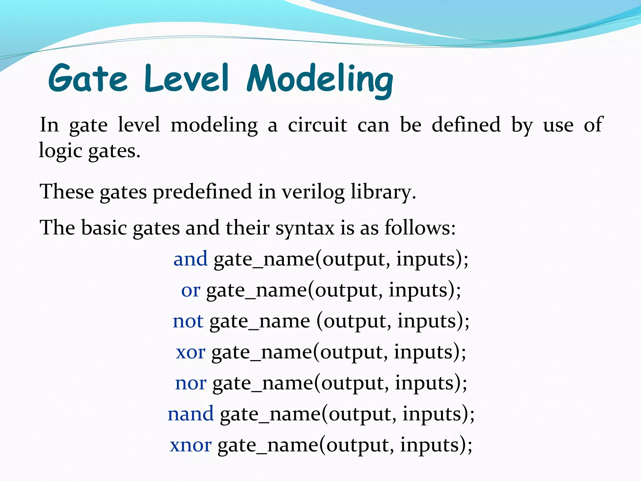
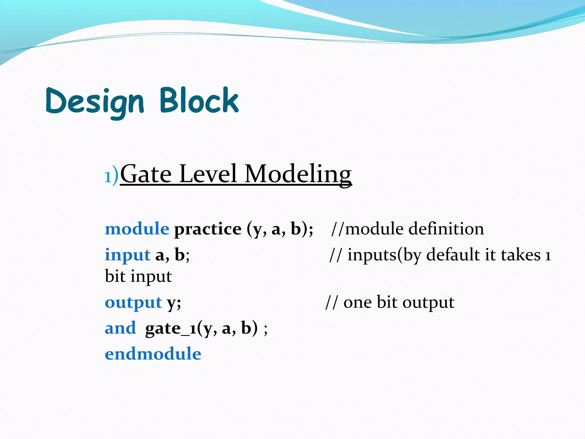
Gate Level Modeling uses predefined logic gates in Verilog. Syntax for AND, OR, NOT, XOR, and other gates is provided.
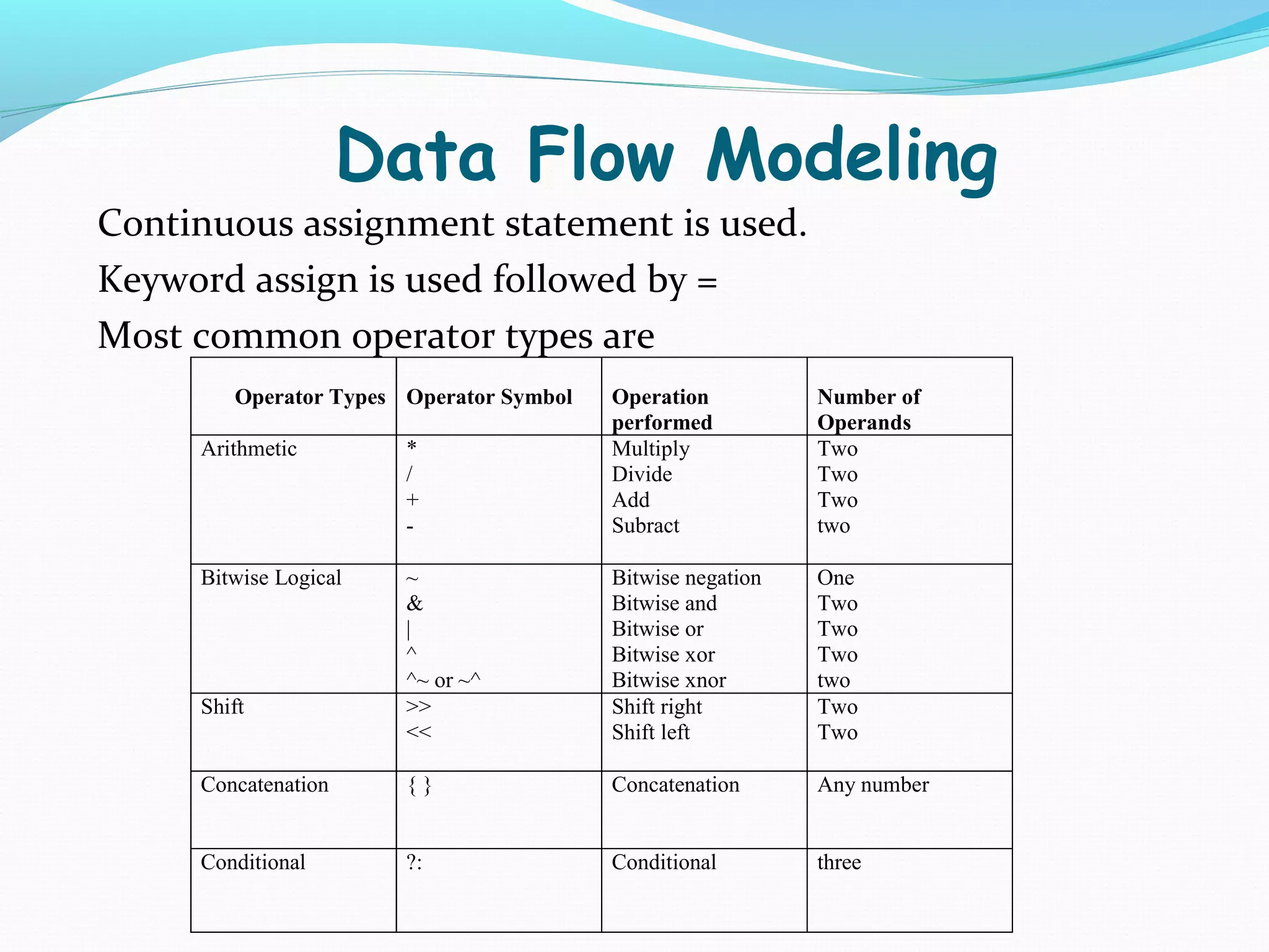
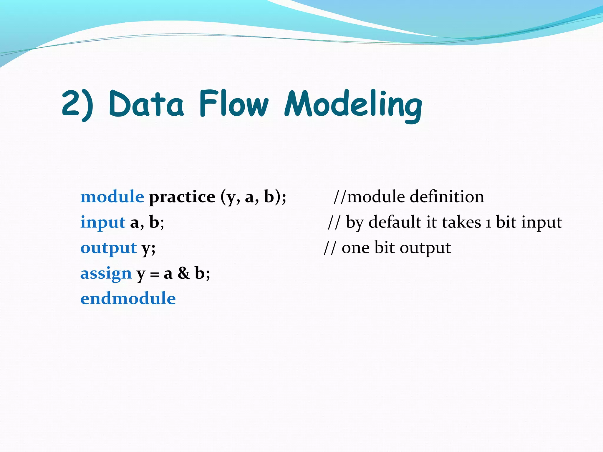
Continuous assignment in Data Flow Modeling uses the 'assign' keyword. Common operator types include arithmetic, bitwise, and conditional operations.
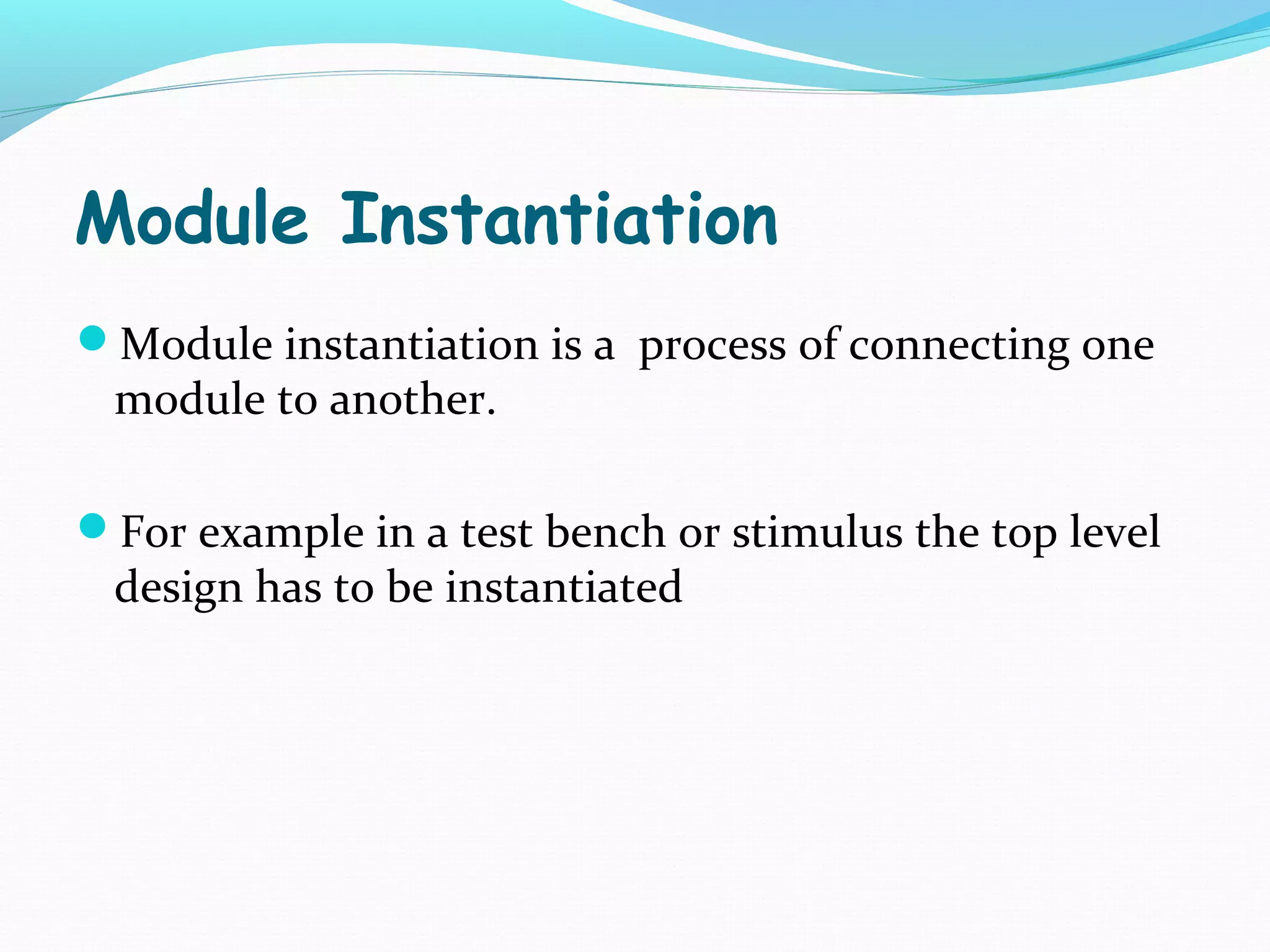
Module instantiation connects one module to another, typically in a test bench for testing.
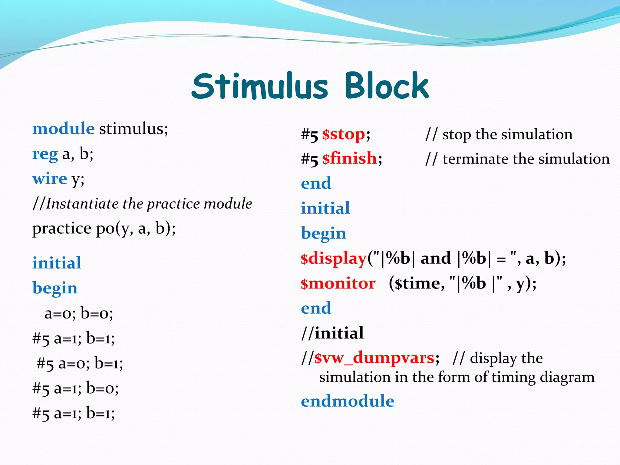
The Stimulus Block is the test bench code for circuit validation, displaying outputs based on inputs.
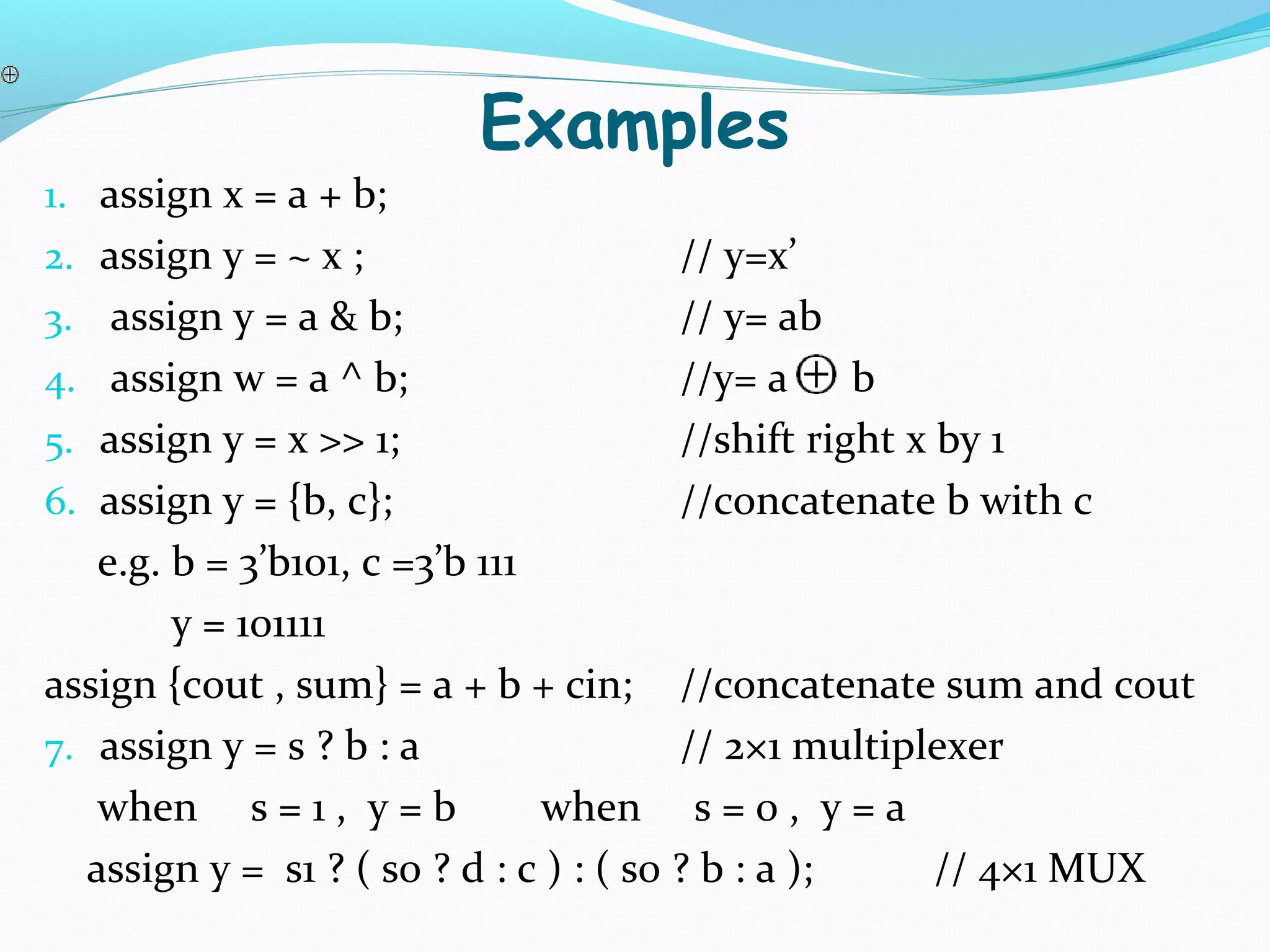
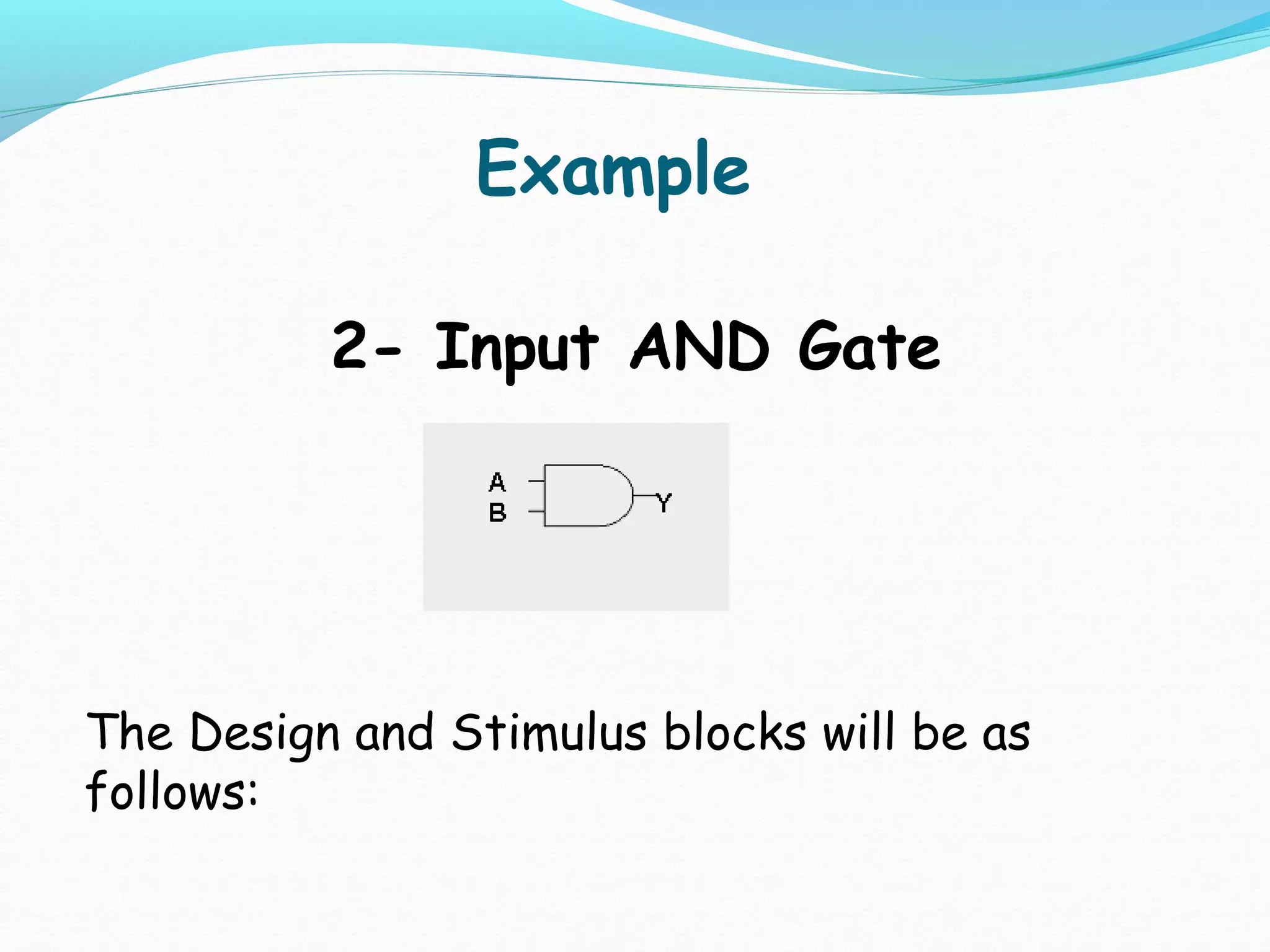
Examples of Gate Level Modeling and Data Flow Modeling in Verilog for basic logic operations.
The Stimulus Block writes initial conditions for testing, using a 2-input AND gate as an example.
Introduction to the design of a 4-bit ripple carry adder, emphasizing full adder configurations.
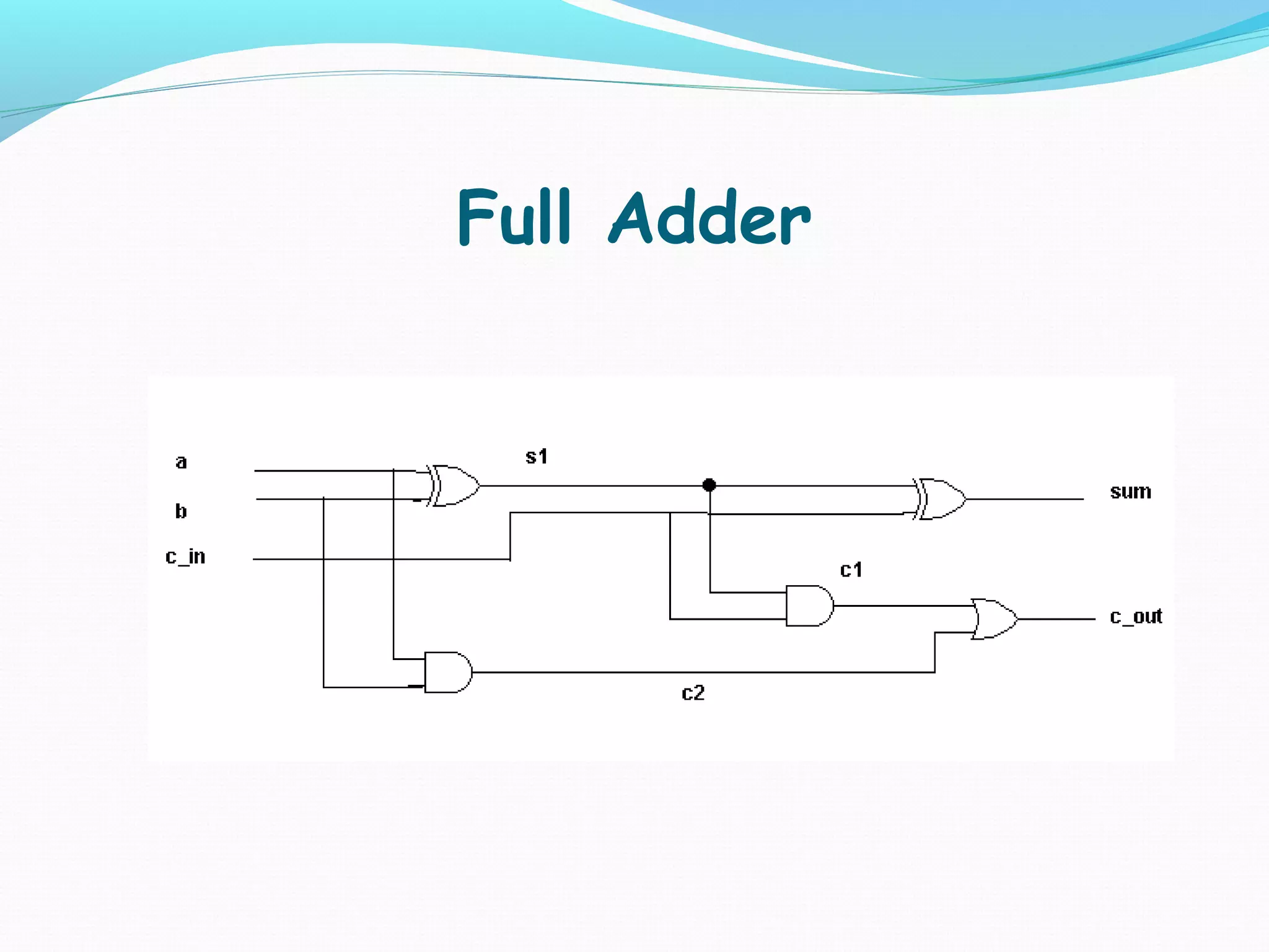
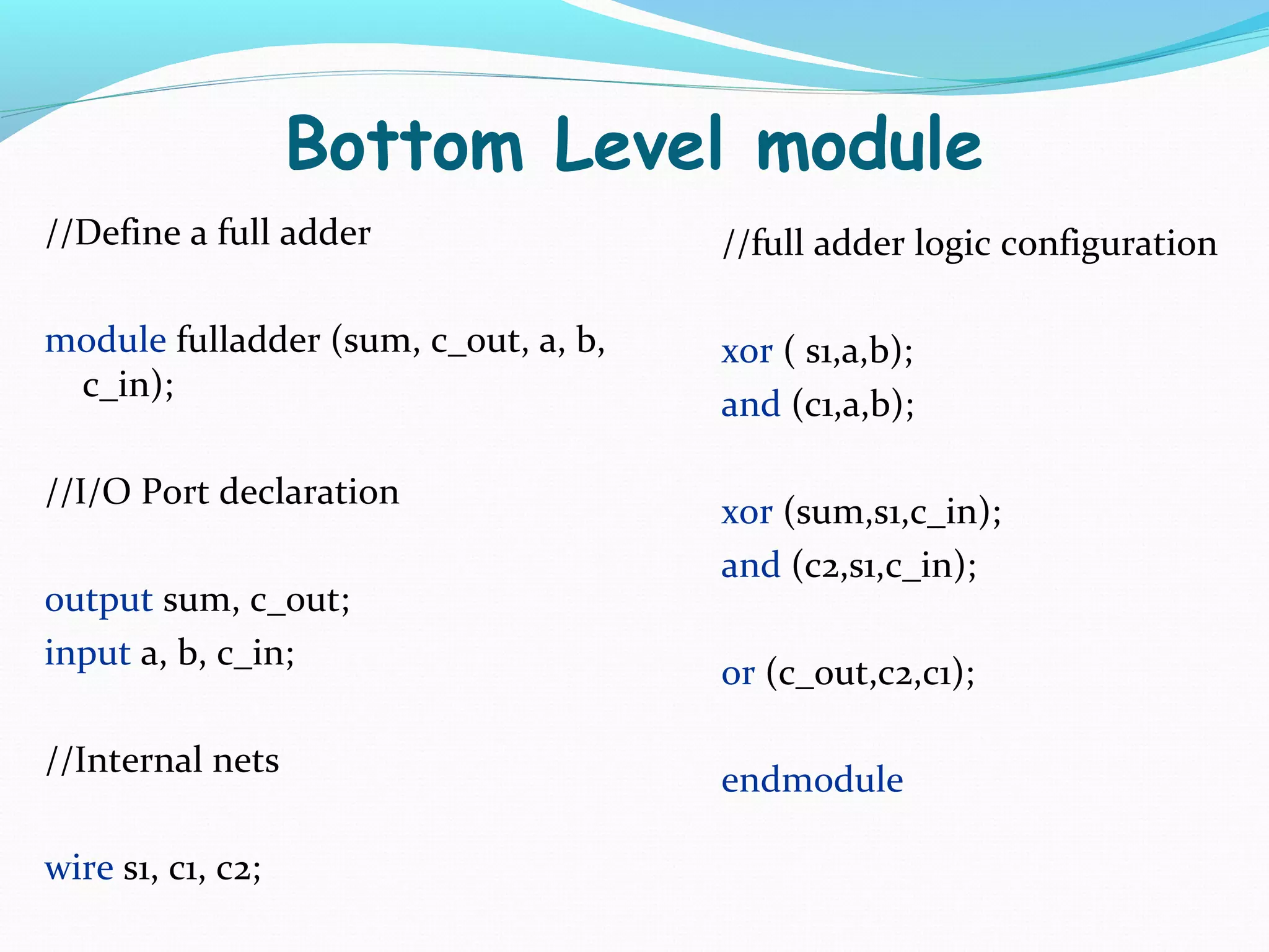
A Full Adder's logic configuration in Verilog, defining module structure and I/O.
Defines the Top Level module for a 4-bit adder, incorporating four 1-bit full adders.
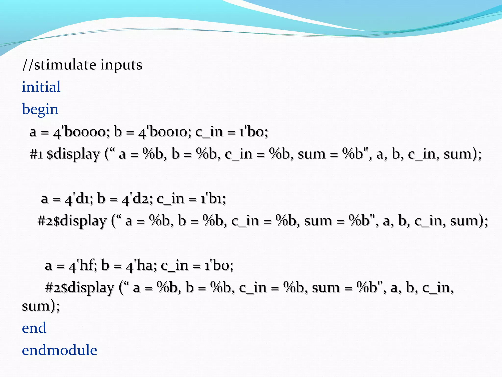
Stimulus setup for the top level module, displaying results of bit addition through various test cases.
Overview of 100 predefined Verilog keywords, emphasizing case sensitivity and syntax rules.
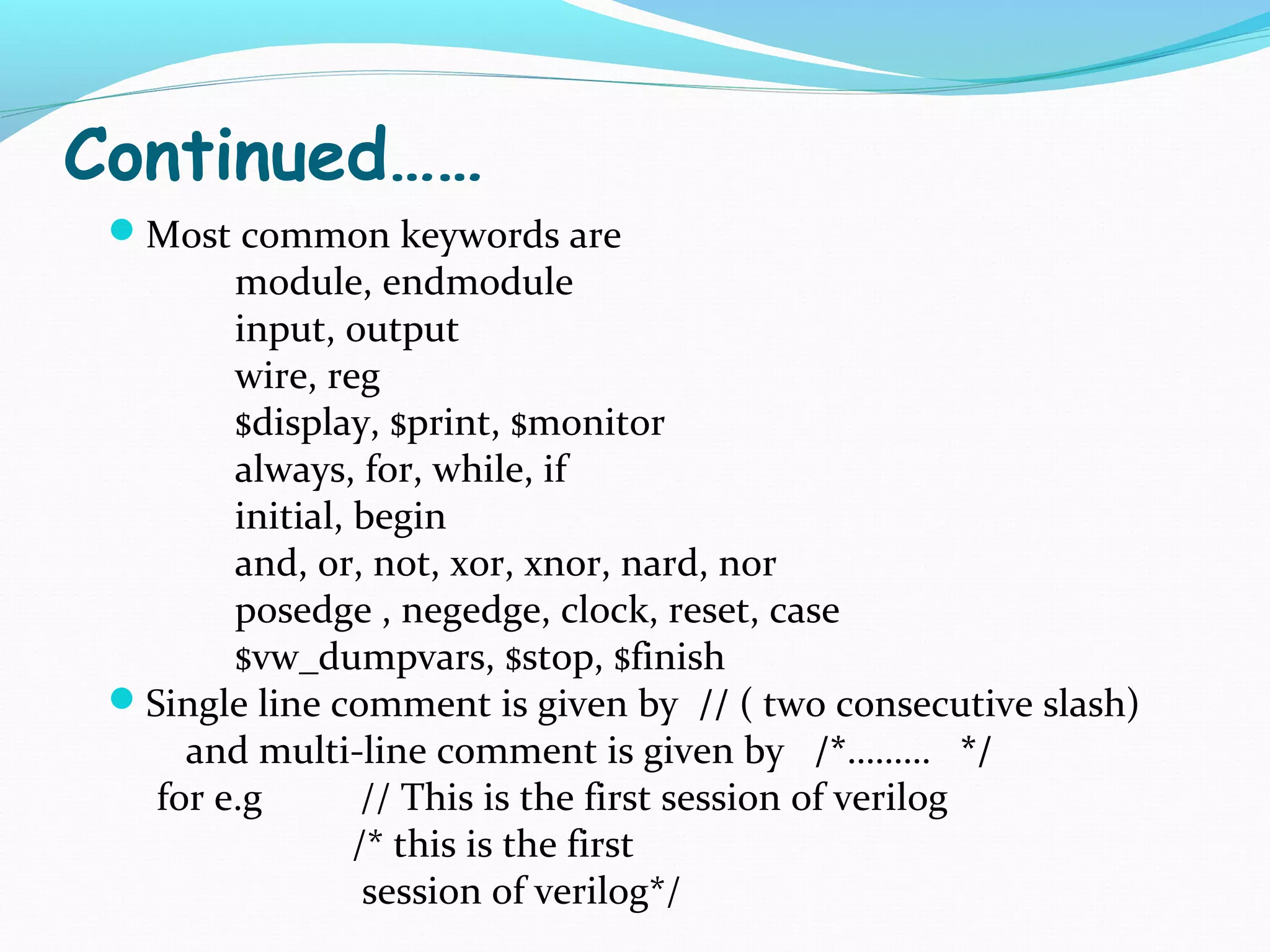
List of essential Verilog keywords with explanations. Includes syntax for comments in Verilog.