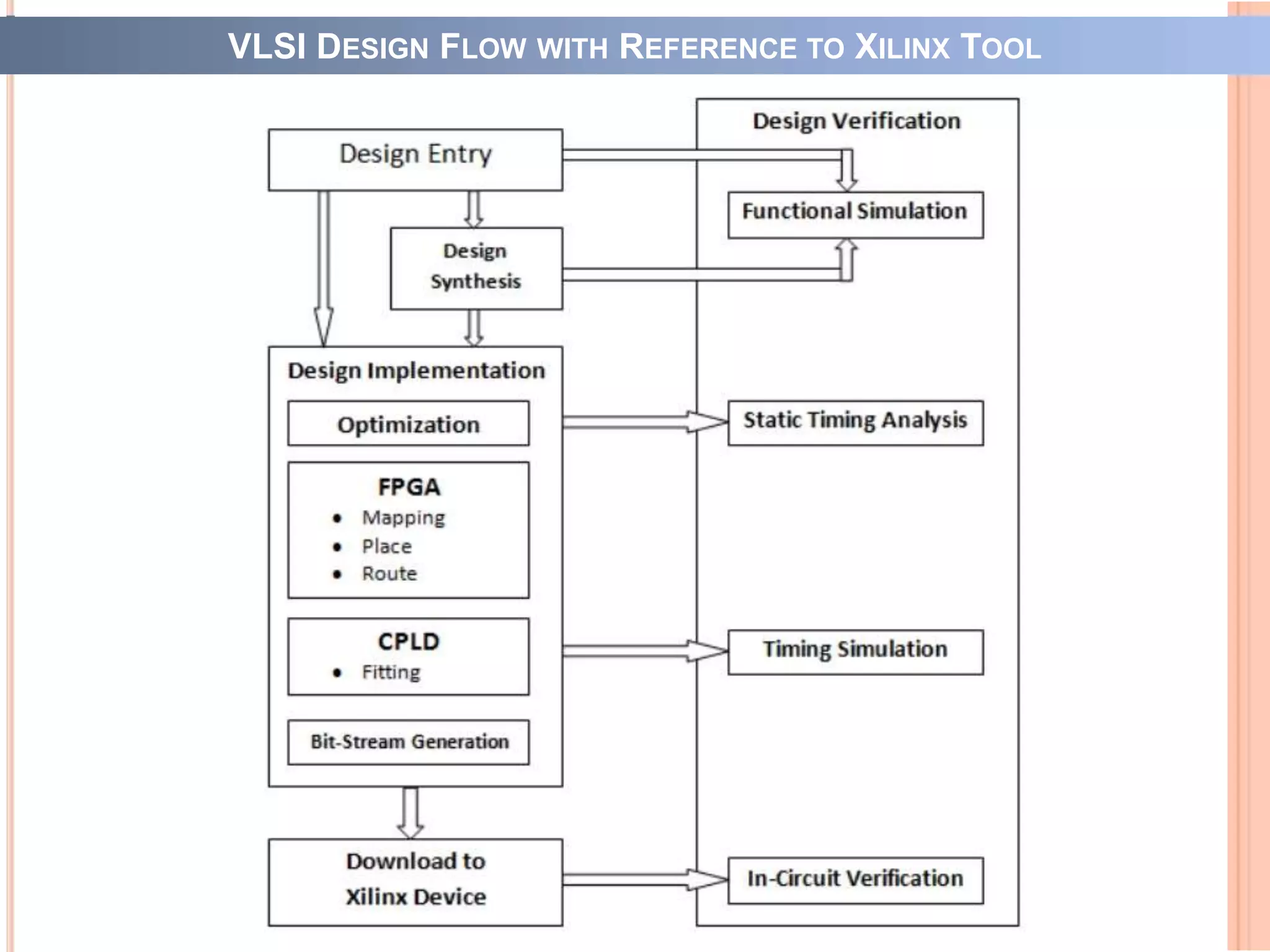
Testing of Logic Circuits document discusses:
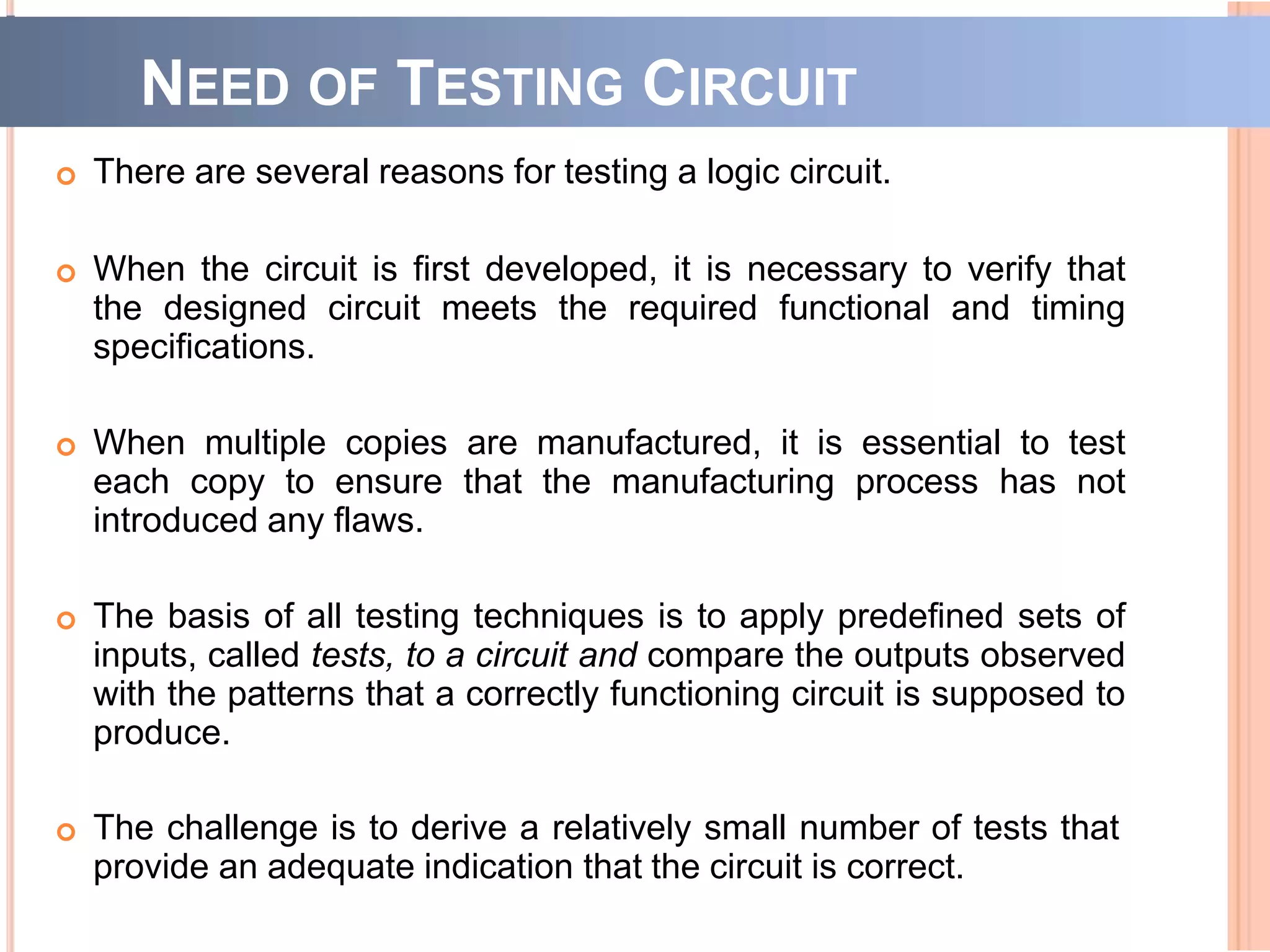
1) The need to test logic circuits when first developed and when manufactured to check for flaws.
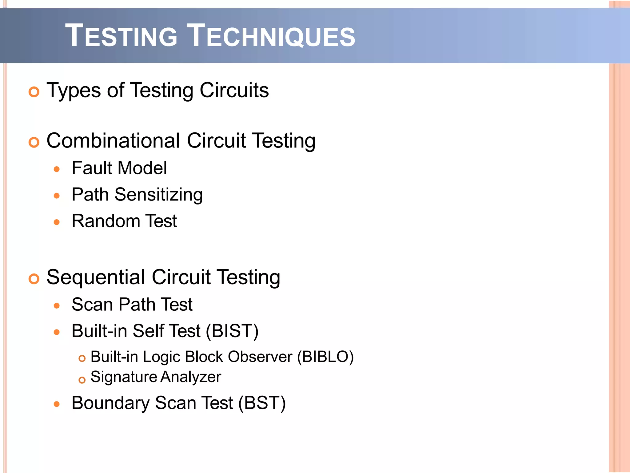
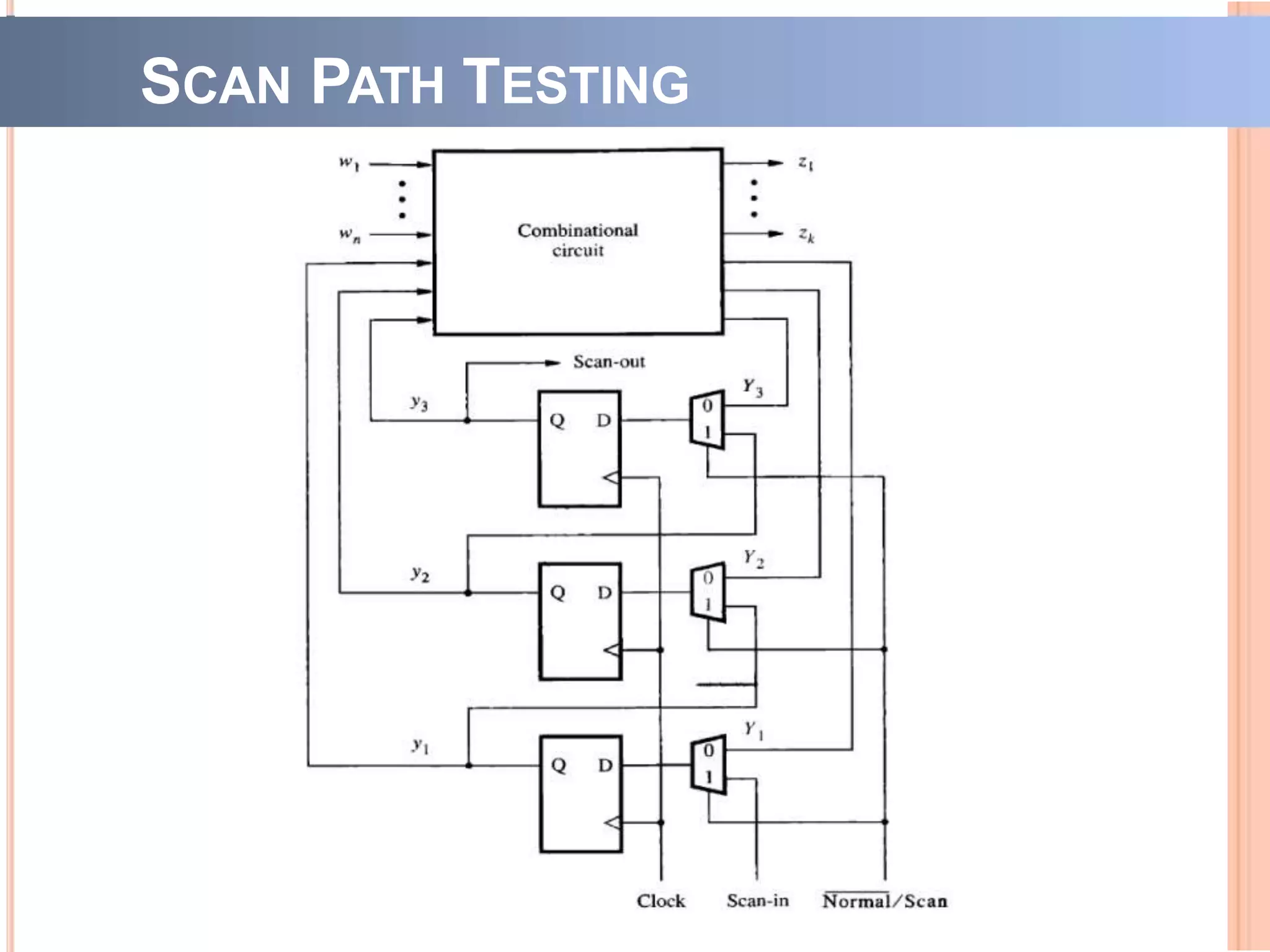
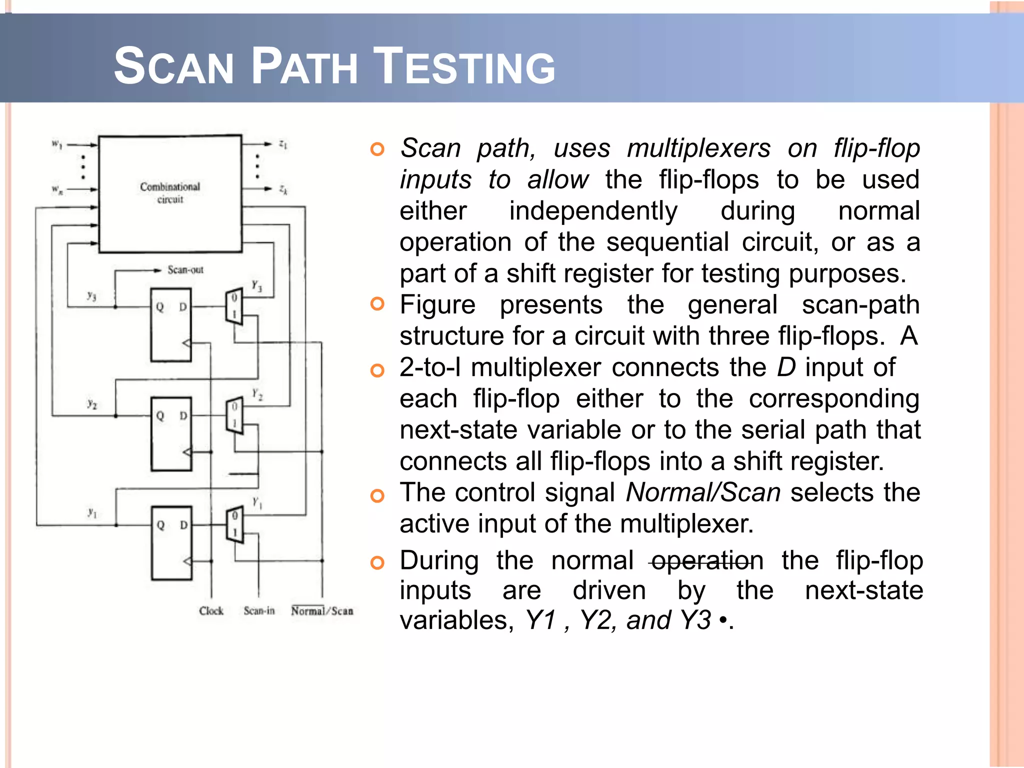
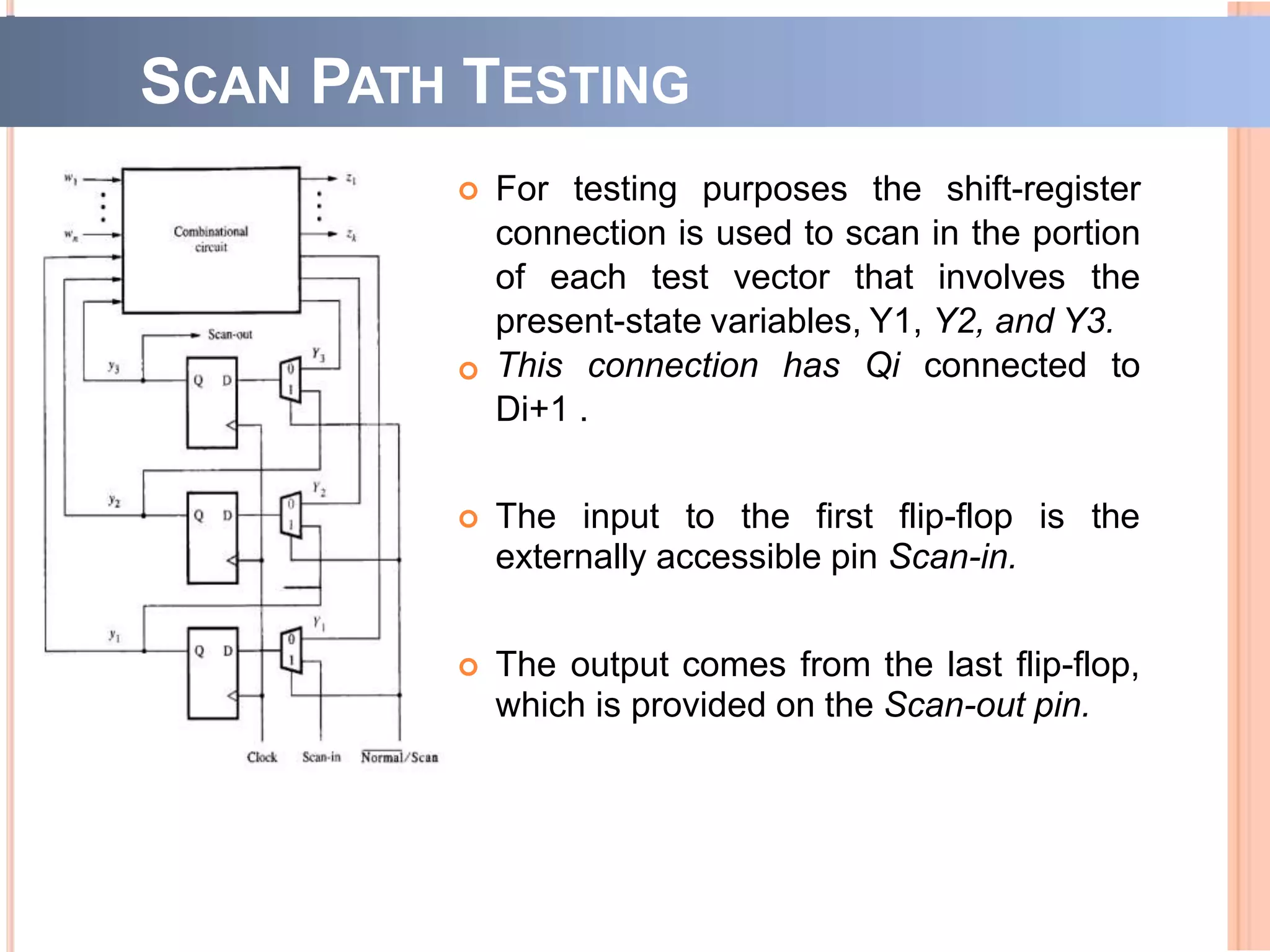
2) Common testing techniques like combinational/sequential circuit testing, fault models, path sensitizing, scan path testing, and boundary scan testing.
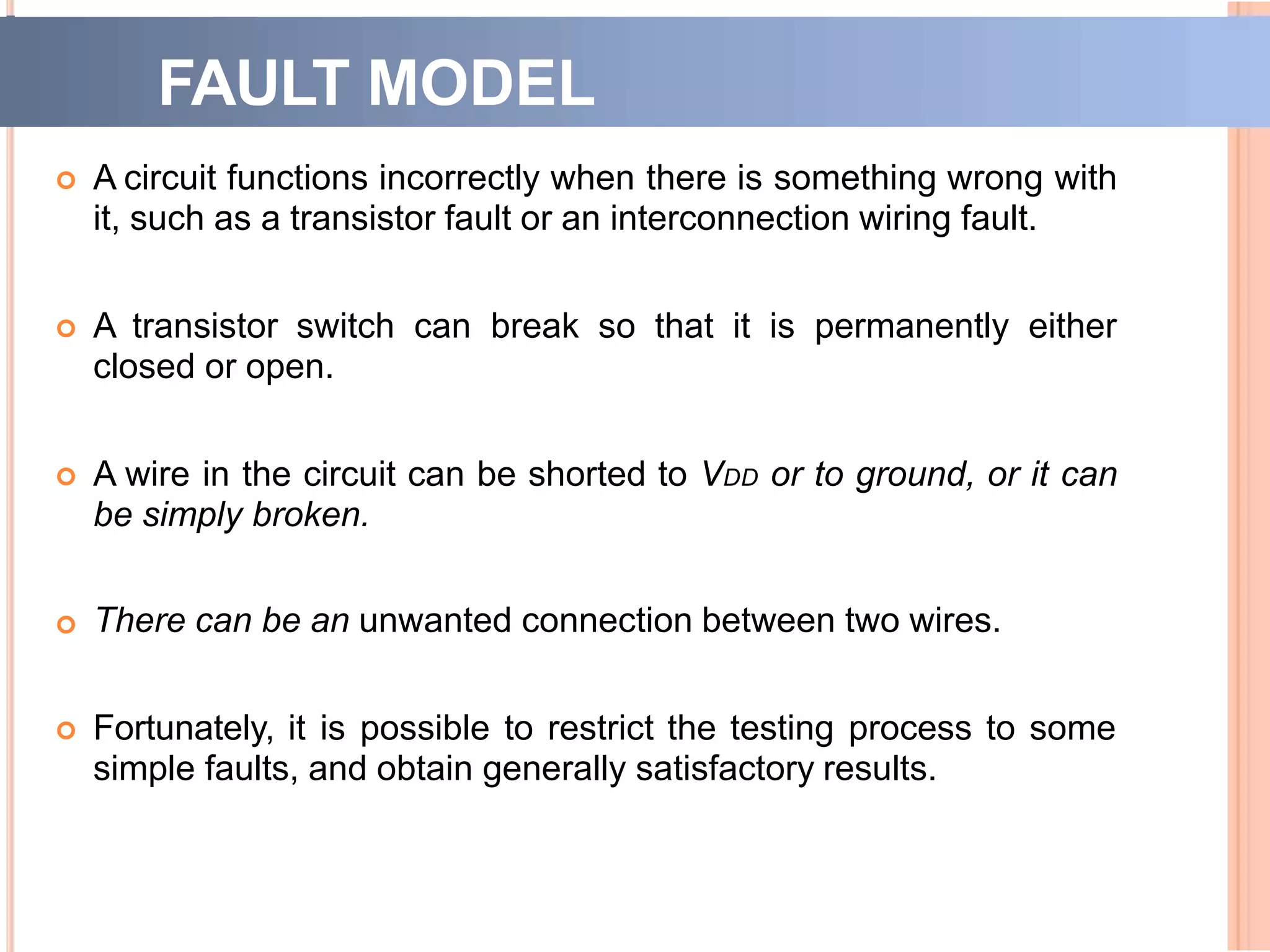
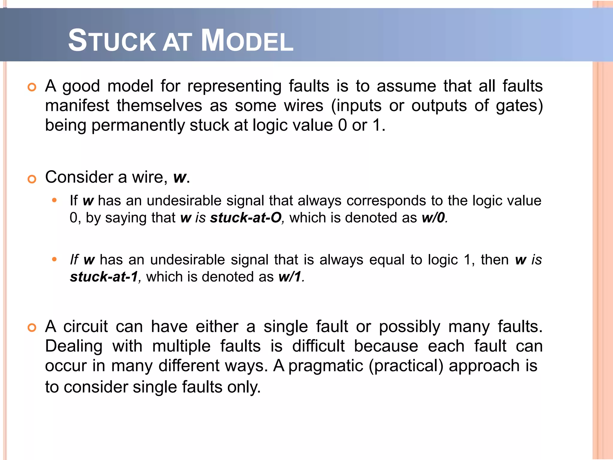
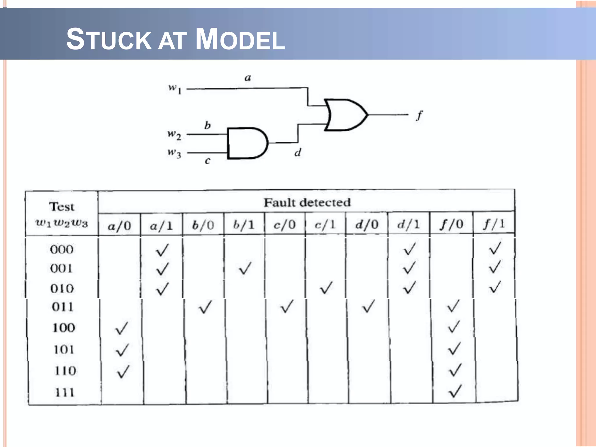
3) Fault models assume faults make wires permanently stuck at logic 0 or 1.
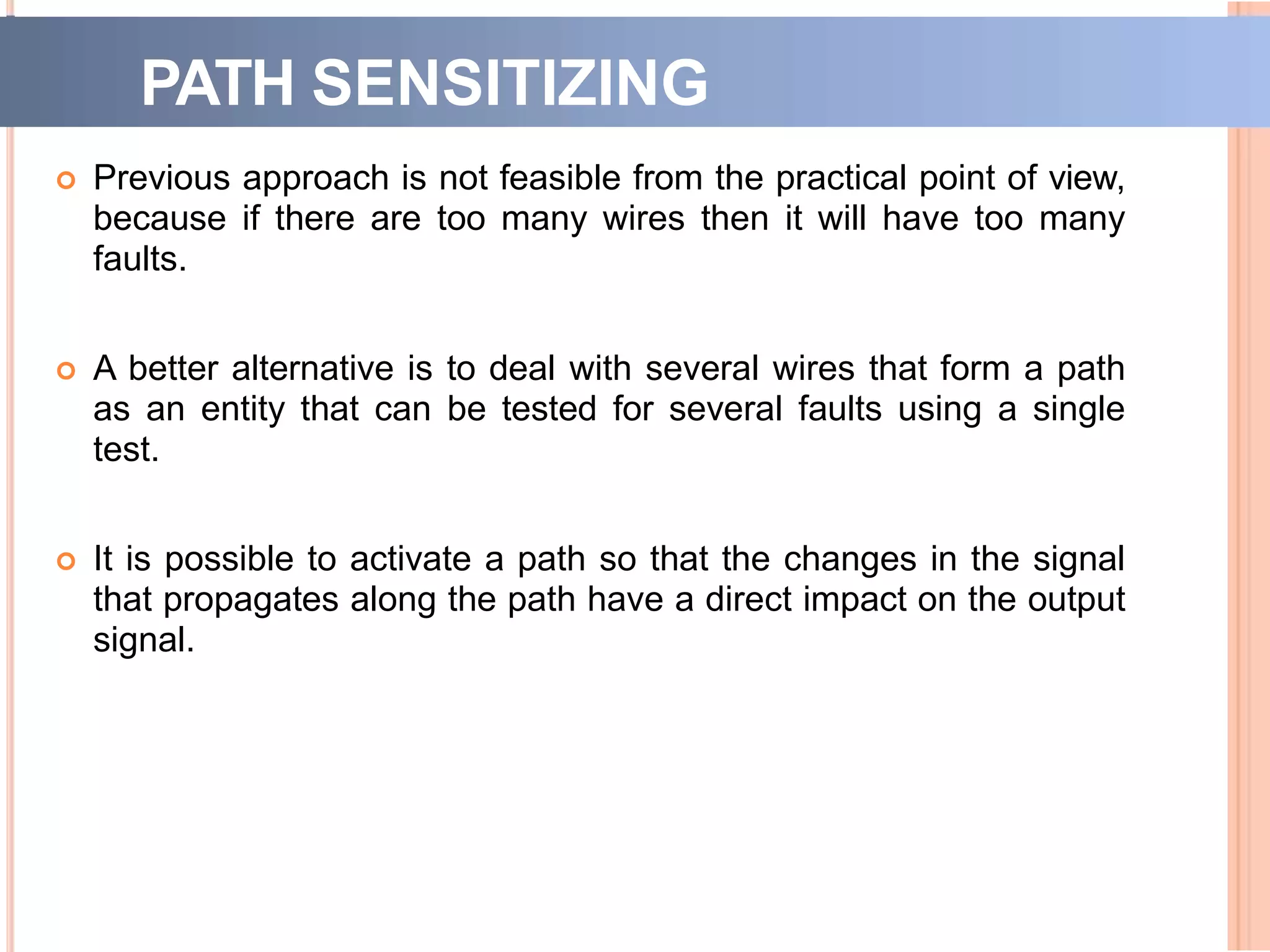
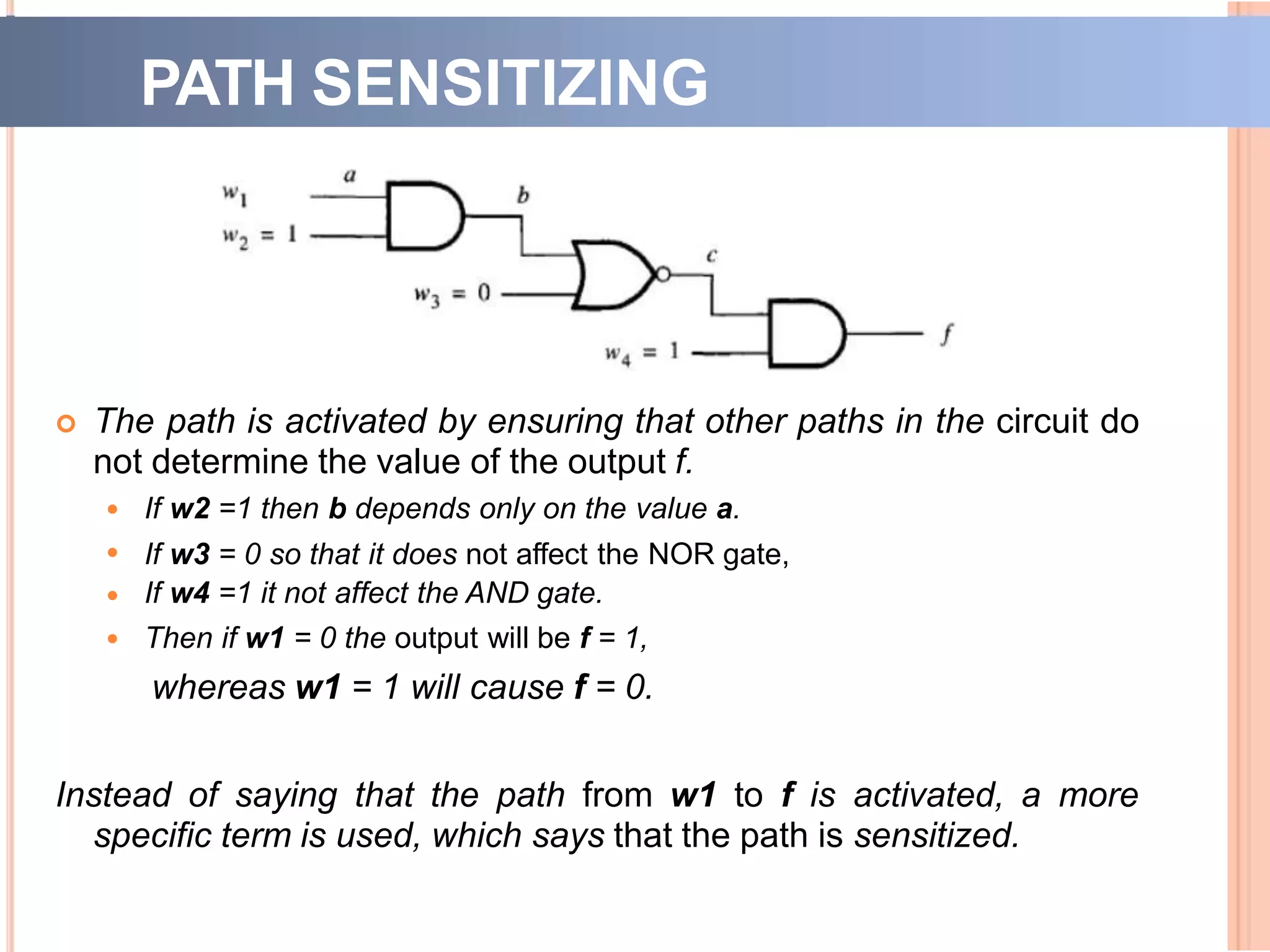
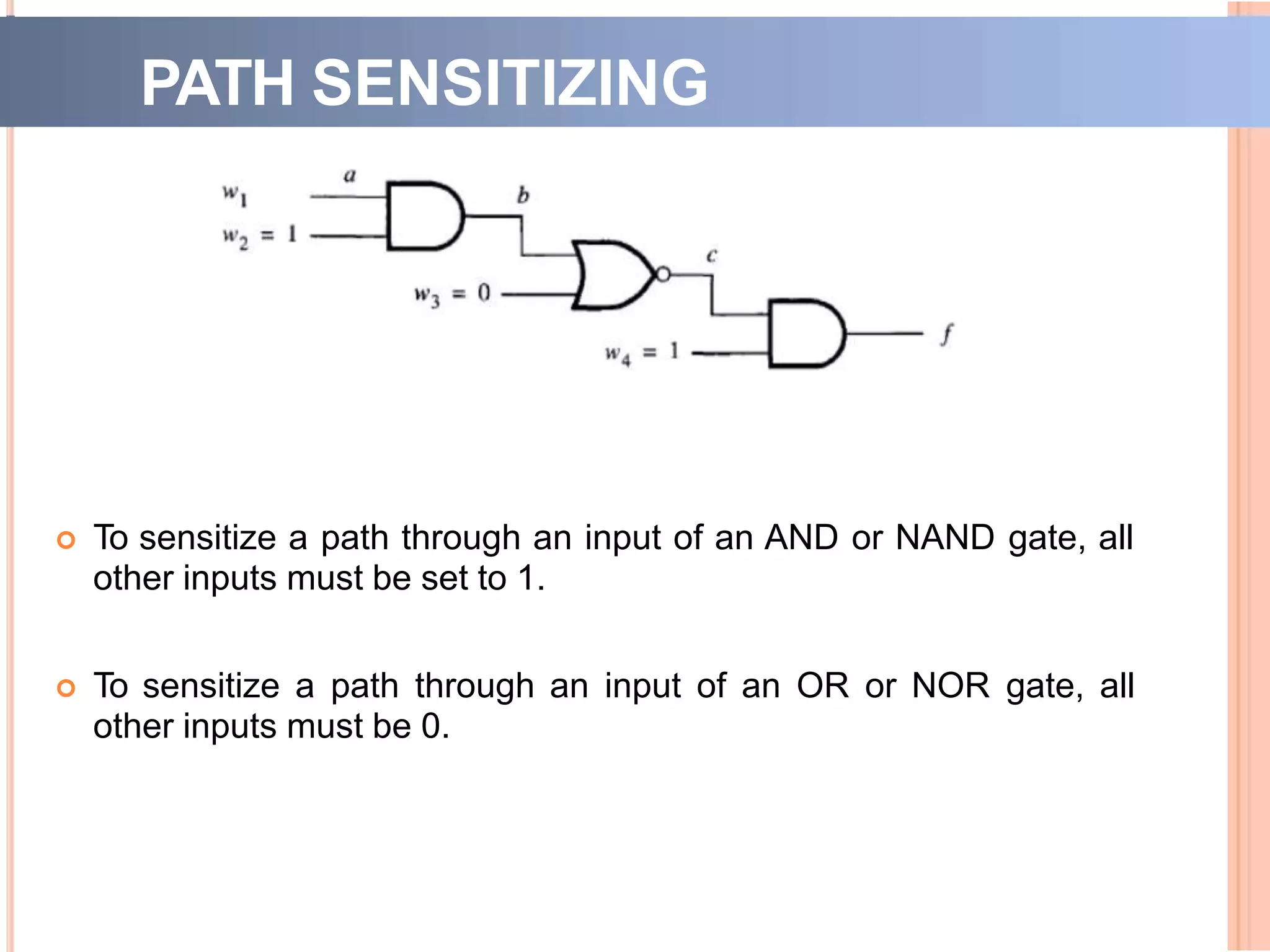
4) Path sensitizing activates paths so signal changes directly impact outputs to test for faults.