A COMPARATIVE STUDY ON RIGID CONNECTION DESIGN OF FRAMED MULTI STOREYED STEEL...
Ultra BGA Fact Sheet Asia
1. Ultra BGAUltra BGA®® SubstratesSubstrates
Patented “build-up on a heat sink” structure
Integrated thermal management
Multi-layer, multi-tier, multi-cavity
20 mm to 50 mm body sizes
Sub 50 µm line and space capability
Via-in-pad and 80 µm via diameters
Meets or beats Jedec Level 3 rel testing
Very low cost tooling for custom designs
Electrolytic Ni/Au with no plating tails
High yield photo lithography process
Volume manufacturing in Shenzhen, China
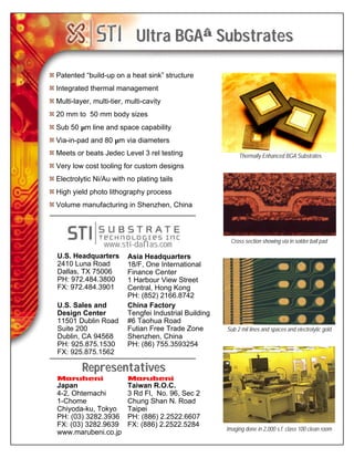
Imaging done in 2,000 s.f. class 100 clean room
Cross section showing via in solder ball pad
www.www.stisti--dallasdallas.com.com
U.S. Headquarters
2410 Luna Road
Dallas, TX 75006
PH: 972.484.3800
FX: 972.484.3901
U.S. Sales and
Design Center
11501 Dublin Road
Suite 200
Dublin, CA 94568
PH: 925.875.1530
FX: 925.875.1562
Asia Headquarters
18/F, One International
Finance Center
1 Harbour View Street
Central, Hong Kong
PH: (852) 2166.8742
China Factory
Tengfei Industrial Building
#6 Taohua Road
Futian Free Trade Zone
Shenzhen, China
PH: (86) 755.3593254
RepresentativesRepresentatives
Taiwan R.O.C.
3 Rd Fl, No. 96, Sec 2
Chung Shan N. Road
Taipei
PH: (886) 2.2522.6607
FX: (886) 2.2522.5284
Thermally Enhanced BGA Substrates
Sub 2 mil lines and spaces and electrolytic gold
Japan
4-2, Ohtemachi
1-Chome
Chiyoda-ku, Tokyo
PH: (03) 3282.3936
FX: (03) 3282.9639
www.marubeni.co.jp
2. Cross section of assembled Ultra BGA® substrate
= Outer Layer Routing
= Inner Layer Routing
= Wire Bond Finger
= Via Capture Pad
= Via In Pad
= Outer Layer Routing
= Inner Layer Routing
= Wire Bond Finger
= Via Capture Pad
= Via In Pad
Œ
•
Ž
•
•
£
£
£
£
Staggered Bond Finger Pitch
Bond Finger Row Pitch
In-line Bond Finger Pitch
Via Capture Pad Diameter
Via Diameter
Bond Finger Dimensions
Circuit Line/Space Dimensions
Via Formation Method
Circuit Formation Method
0.100
0.650
0.200
0.250
0.100
0.100 x 0.350
0.050 / 0.050
Photo
Photo
Fig. A Fig. B Fig. CFeature / Figure
N/A
N/A
0.150
N/A
N/A
0.100 x 0.350
0.050 / 0.050
Photo
Photo
0.125
0.400
0.250
N/A
N/A
0.100 x 0.350
0.050 / 0.050
Photo
Photo
Œ
•
Ž
Ball Pad Side
Cavity Side
Œ
•
Ž
Ball Pad Side
Cavity Side
Ball Pad Side
Cavity Side
Ž
Ball Pad Side
Cavity Side
Ž
Figure A. Figure B. Figure C.
Key To Figures
Wire bond pad configurations
Dielectric Properties Testing Summary
Reliability (Precon Level 3)
Temp Cycle
HAST
HTS
Integrity (Precon Level 3)
PCT
MSL
Assembly
Wire Bond
Coplanarity
Ball Shear
Die Shear
Passed
Passed
Passed
Passed
Passed
Passed
Passed
Passed
Passed
1,000 Cycles, Condition B
3.5v, Biased, 85°C/85RH
175°C, 500 Hours
96 & 168 Hour,
100% RH, 2 Atms
30°C/60%RH, 192 Hour,
3 Reflows, 220°C Peak
Auto Mode, 1 Mil Au Wire
Pre & Post Assembly
Pre & Post Precon Level 3
Post Assembly (EOL)
Test Condition Result
Ultra BGAUltra BGA®® Key InformationKey Information
Dielectric Constant (Dk)
at 1 MHz
at 100 MHz
at 1 GHz
Loss Tangent
at 1 MHz
at 100 MHz
at 1 GHz
Dielectric Strength
Surface Resistance (W)
A. 96 hrs / 35C / 90% RH
B. At elevated temp / RTI value
Volume Resistance (W-cm)
A. 96 hrs / 35C / 90% RH
B. At elevated temp / RTI value
Tensile Strength (Mpa)
Elongation
3.83
3.81
3.85
0.0067
0.0086
0.0118
2200 V/mm
4.45 E+11
2.25 E+13
2.23 E+14
1.34 E+11
7,700 psi
5%
IPC 2.5.5.9
IPC 2.5.5.9
IPC 2.5.6.2
IPC 2.5.17.1A
IPC 2.5.17.1A
IPC 2.4.18.3
IPC 2.4.18.3
Properties Value Test Method
In-line Bond
Finger Diagram
Staggered Row
Diagram – External
Routing Only
Staggered Row
Diagram – Internal
Layer Routing
Œ
•
Ž
•
•
Ball Pad Side
Cavity Side
Œ
•
Ž
•
•
Ball Pad Side
Cavity Side
•
Ž