INTRODUCTION
In 1931, whileconducting research for his masters at the technical
college of Berlin, Ernst Ruska and Max Knoll designed first TEM.
This is much like a slide projector but the basic difference is light
microscope uses Beam of Light whereas TEM uses Beam of electron.
TEM is a microscopy technique in which a beam of electrons is
transmitted through an ultra thin specimen, interacting with the
specimen as it passes through.
The wavelength of electron is about 0.005nm which is 100000x
shorter than that of light, hence TEM has better resolution than that of
the light microscope, of about 1000 times.
The TEM image shows the size, shape, crystalline or amorphous
structure, and orientation of the sample's components.
14.
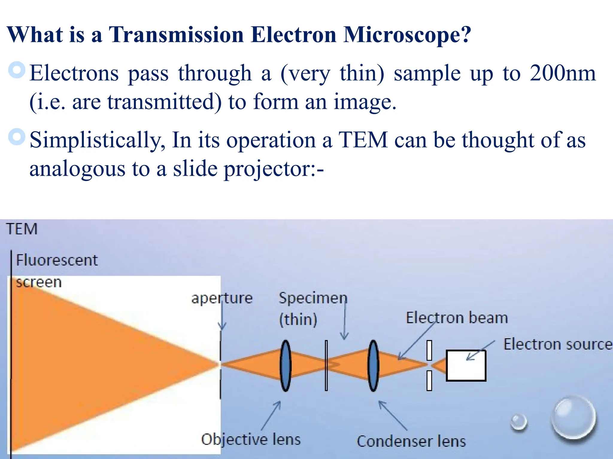
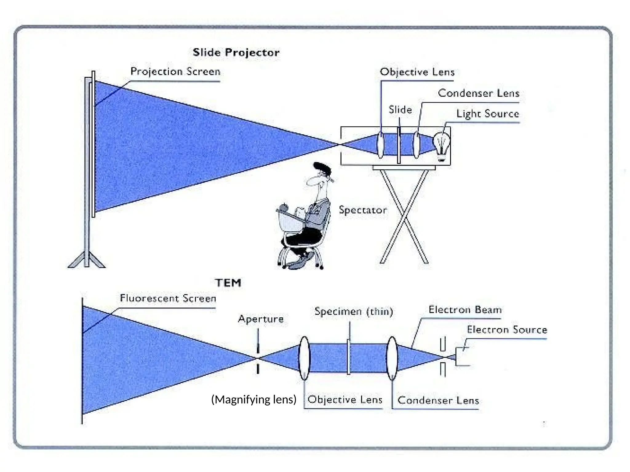
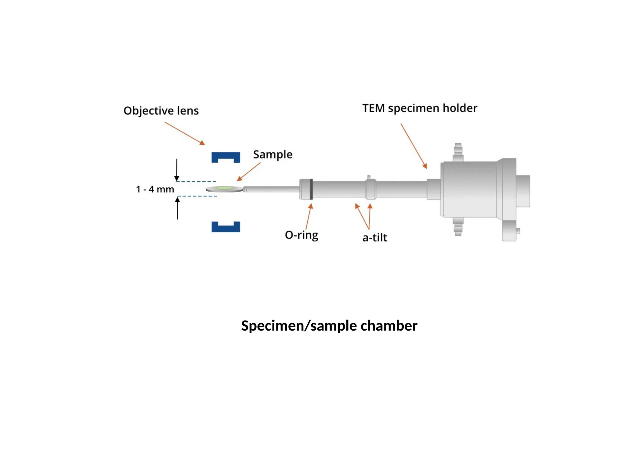
What is aTransmission Electron Microscope?
Electrons pass through a (very thin) sample up to 200nm
(i.e. are transmitted) to form an image.
Simplistically, In its operation a TEM can be thought of as
analogous to a slide projector:-
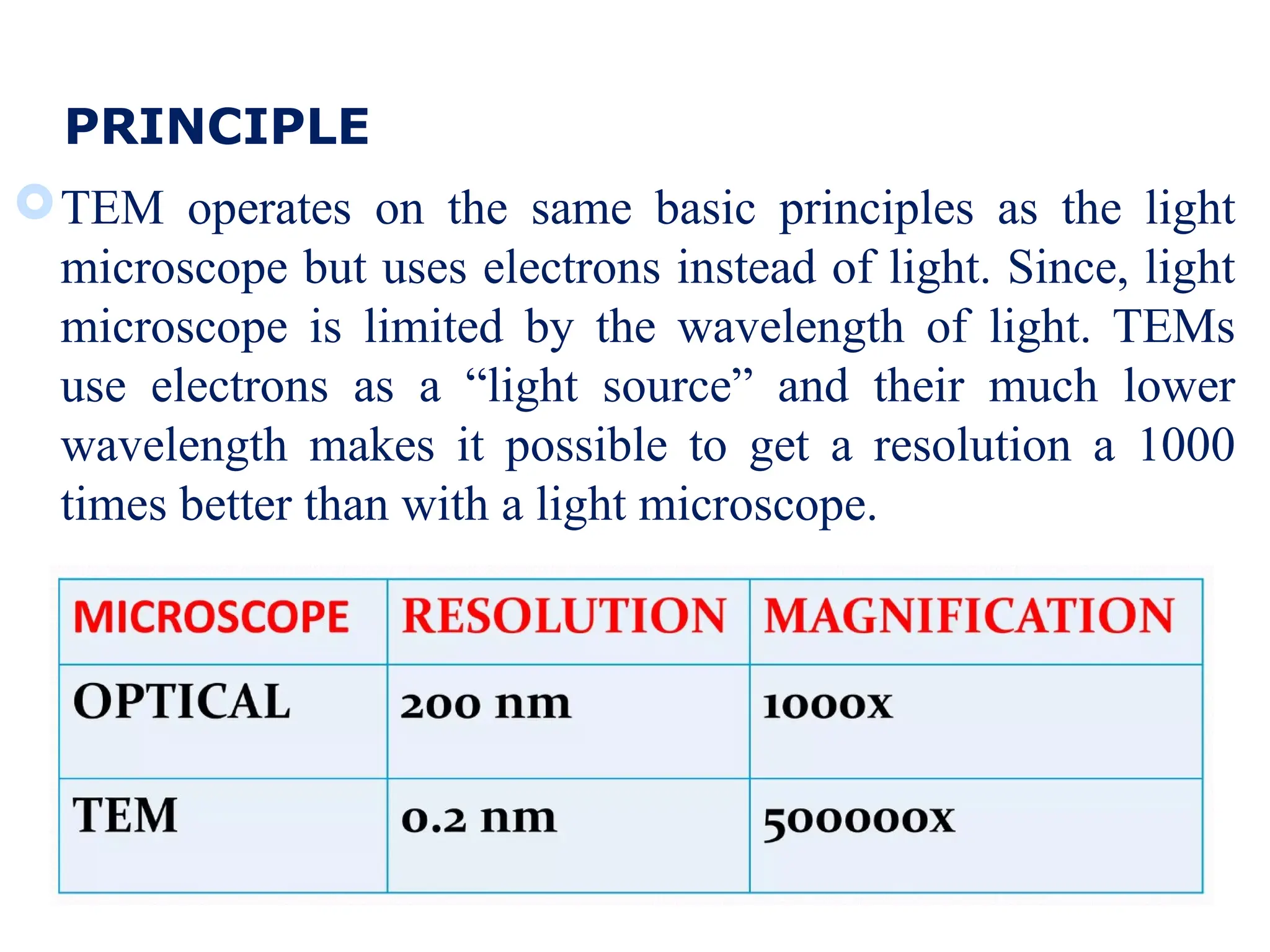
PRINCIPLE
TEM operates onthe same basic principles as the light
microscope but uses electrons instead of light. Since, light
microscope is limited by the wavelength of light. TEMs
use electrons as a “light source” and their much lower
wavelength makes it possible to get a resolution a 1000
times better than with a light microscope.
17.
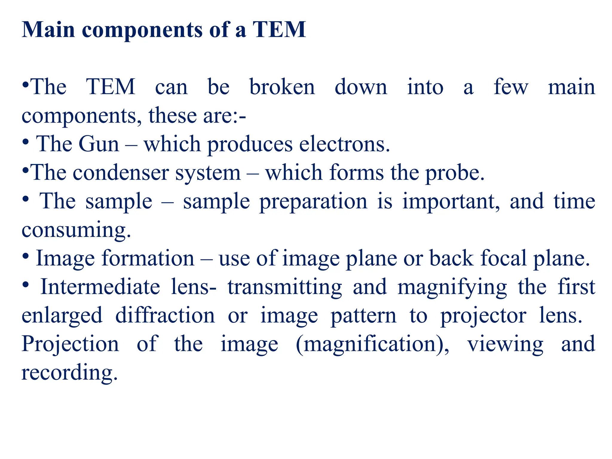
Main components ofa TEM
•The TEM can be broken down into a few main
components, these are:-
• The Gun – which produces electrons.
•The condenser system – which forms the probe.
• The sample – sample preparation is important, and time
consuming.
• Image formation – use of image plane or back focal plane.
• Intermediate lens- transmitting and magnifying the first
enlarged diffraction or image pattern to projector lens.
Projection of the image (magnification), viewing and
recording.
19.
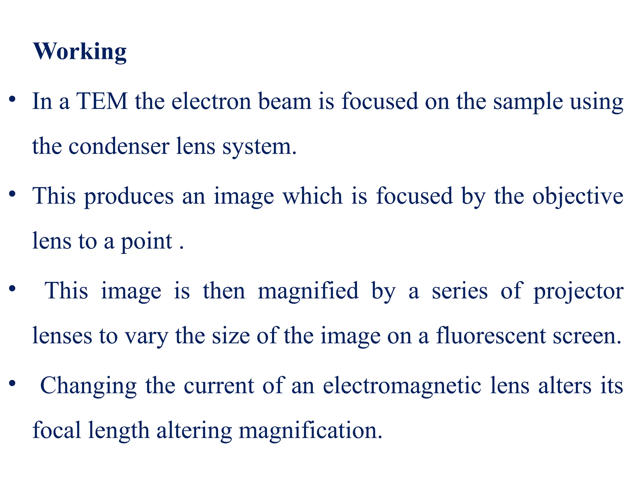
Working
• In aTEM the electron beam is focused on the sample using
the condenser lens system.
• This produces an image which is focused by the objective
lens to a point .
• This image is then magnified by a series of projector
lenses to vary the size of the image on a fluorescent screen.
• Changing the current of an electromagnetic lens alters its
focal length altering magnification.
20.
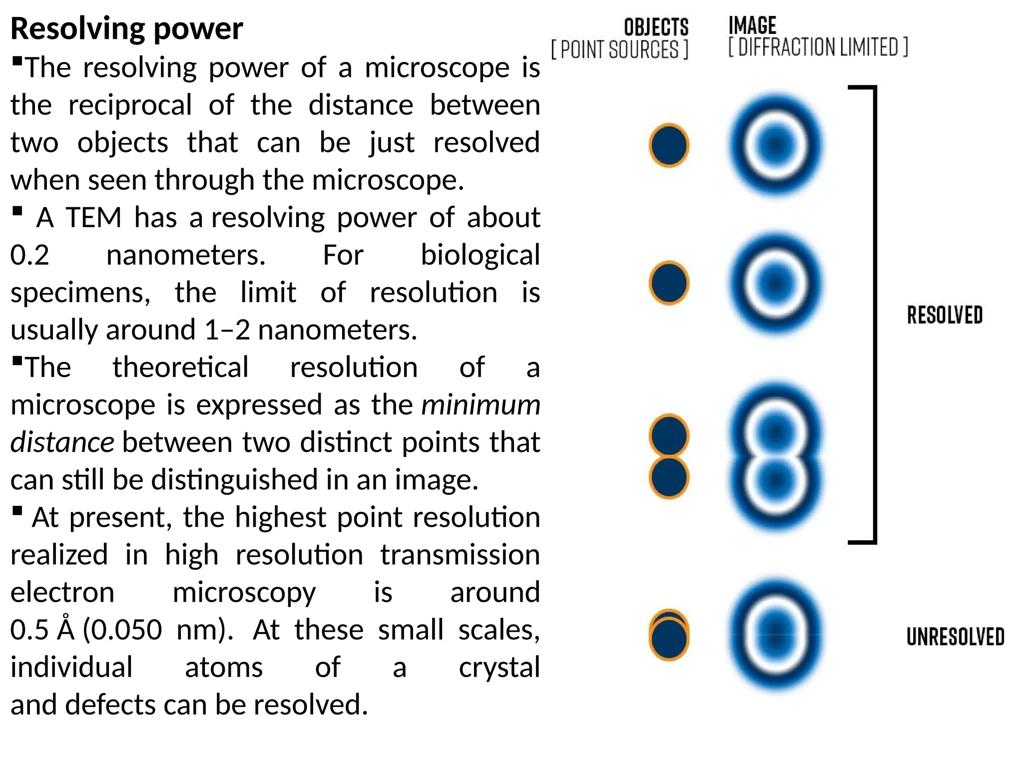
Resolving power
The resolvingpower of a microscope is
the reciprocal of the distance between
two objects that can be just resolved
when seen through the microscope.
A TEM has a resolving power of about
0.2 nanometers. For biological
specimens, the limit of resolution is
usually around 1–2 nanometers.
The theoretical resolution of a
microscope is expressed as the minimum
distance between two distinct points that
can still be distinguished in an image.
At present, the highest point resolution
realized in high resolution transmission
electron microscopy is around
0.5 Å (0.050 nm). At these small scales,
individual atoms of a crystal
and defects can be resolved.
21.
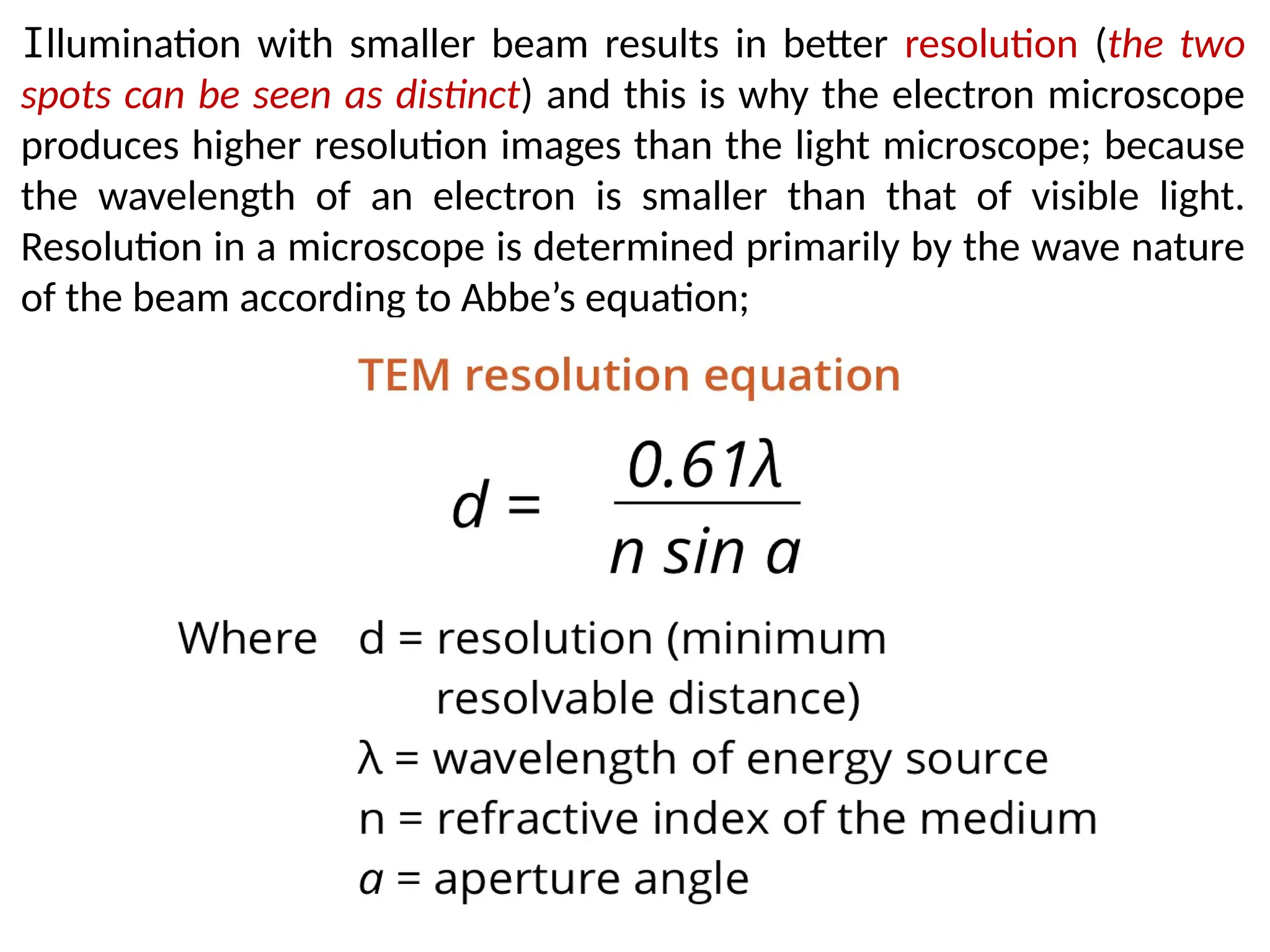
Illumination with smallerbeam results in better resolution (the two
spots can be seen as distinct) and this is why the electron microscope
produces higher resolution images than the light microscope; because
the wavelength of an electron is smaller than that of visible light.
Resolution in a microscope is determined primarily by the wave nature
of the beam according to Abbe’s equation;
22.
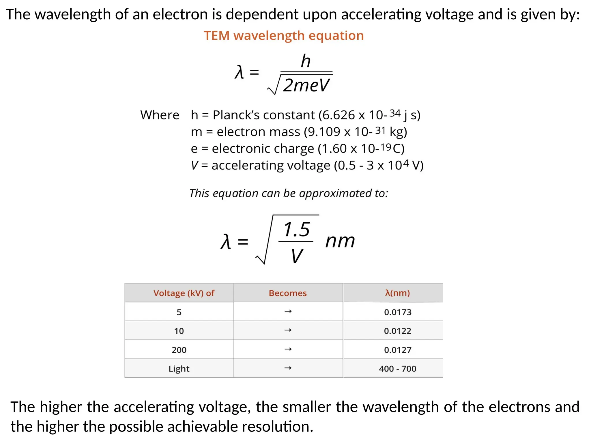
The wavelength ofan electron is dependent upon accelerating voltage and is given by:
The higher the accelerating voltage, the smaller the wavelength of the electrons and
the higher the possible achievable resolution.
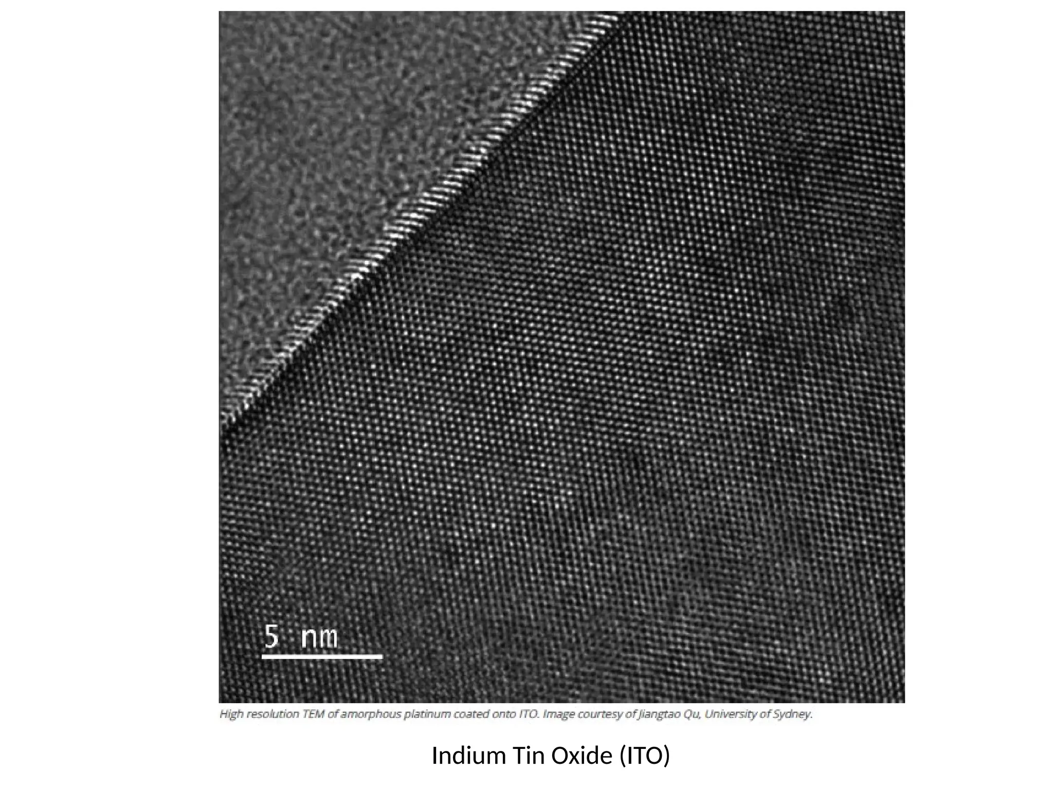
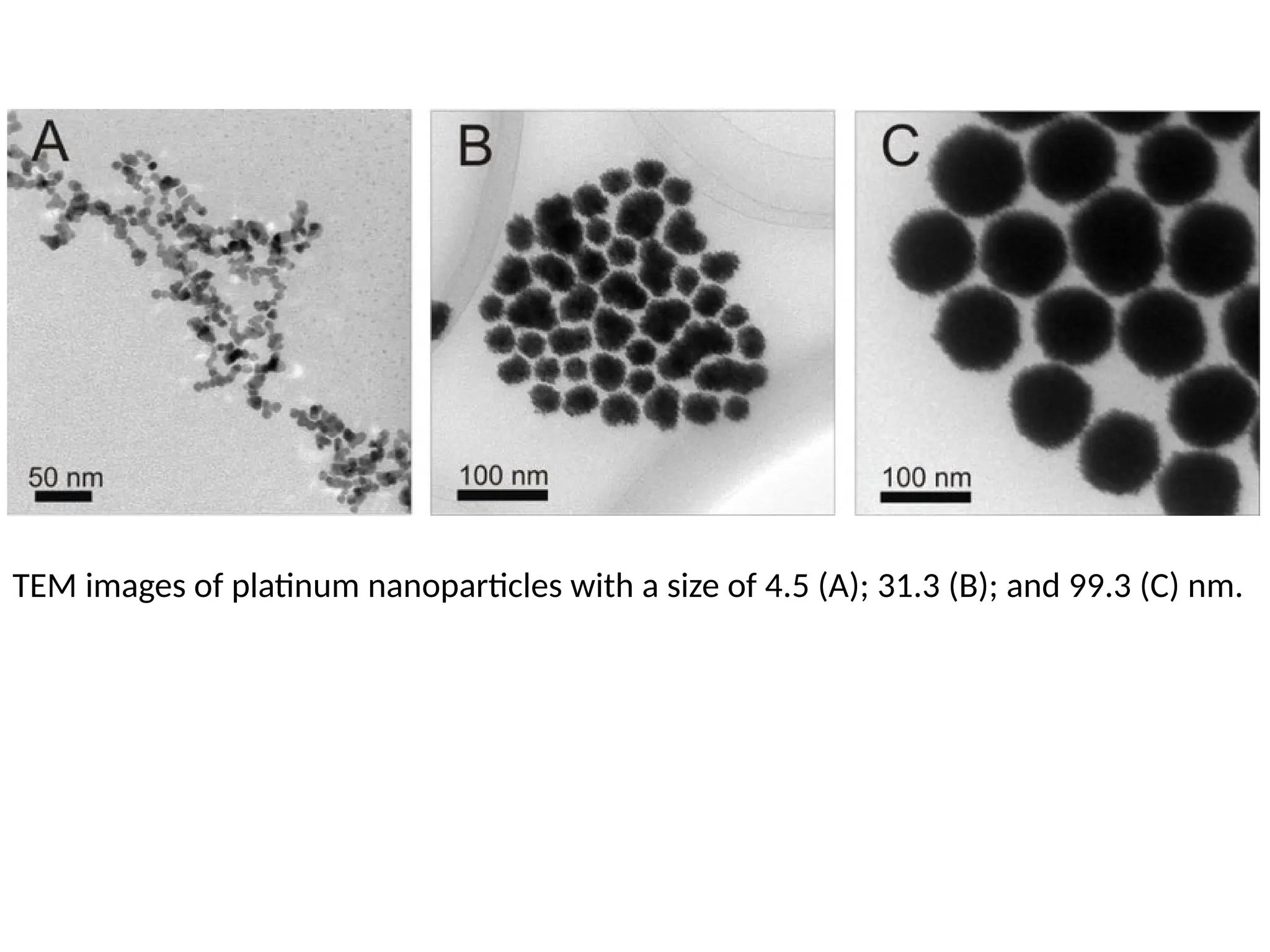
TEM images ofplatinum nanoparticles with a size of 4.5 (A); 31.3 (B); and 99.3 (C) nm.
25.
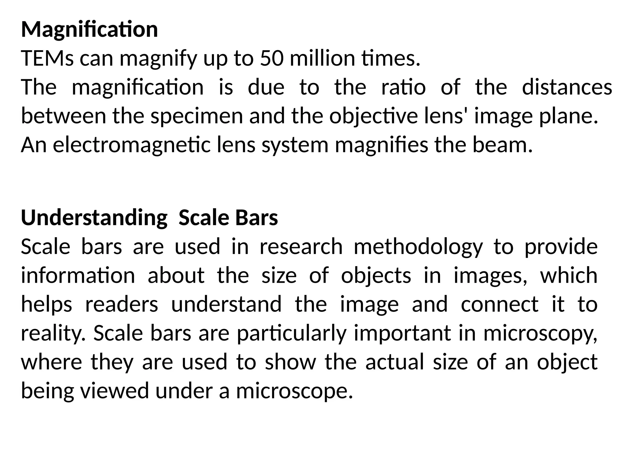
Magnification
TEMs can magnifyup to 50 million times.
The magnification is due to the ratio of the distances
between the specimen and the objective lens' image plane.
An electromagnetic lens system magnifies the beam.
Understanding Scale Bars
Scale bars are used in research methodology to provide
information about the size of objects in images, which
helps readers understand the image and connect it to
reality. Scale bars are particularly important in microscopy,
where they are used to show the actual size of an object
being viewed under a microscope.
26.
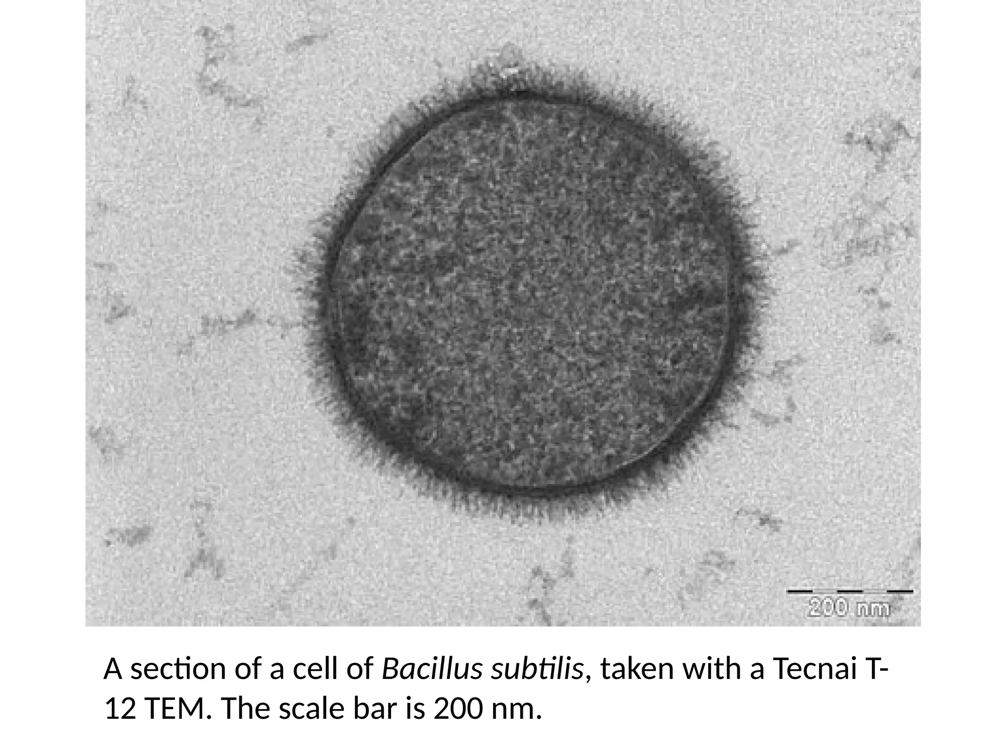
A section ofa cell of Bacillus subtilis, taken with a Tecnai T-
12 TEM. The scale bar is 200 nm.
28.
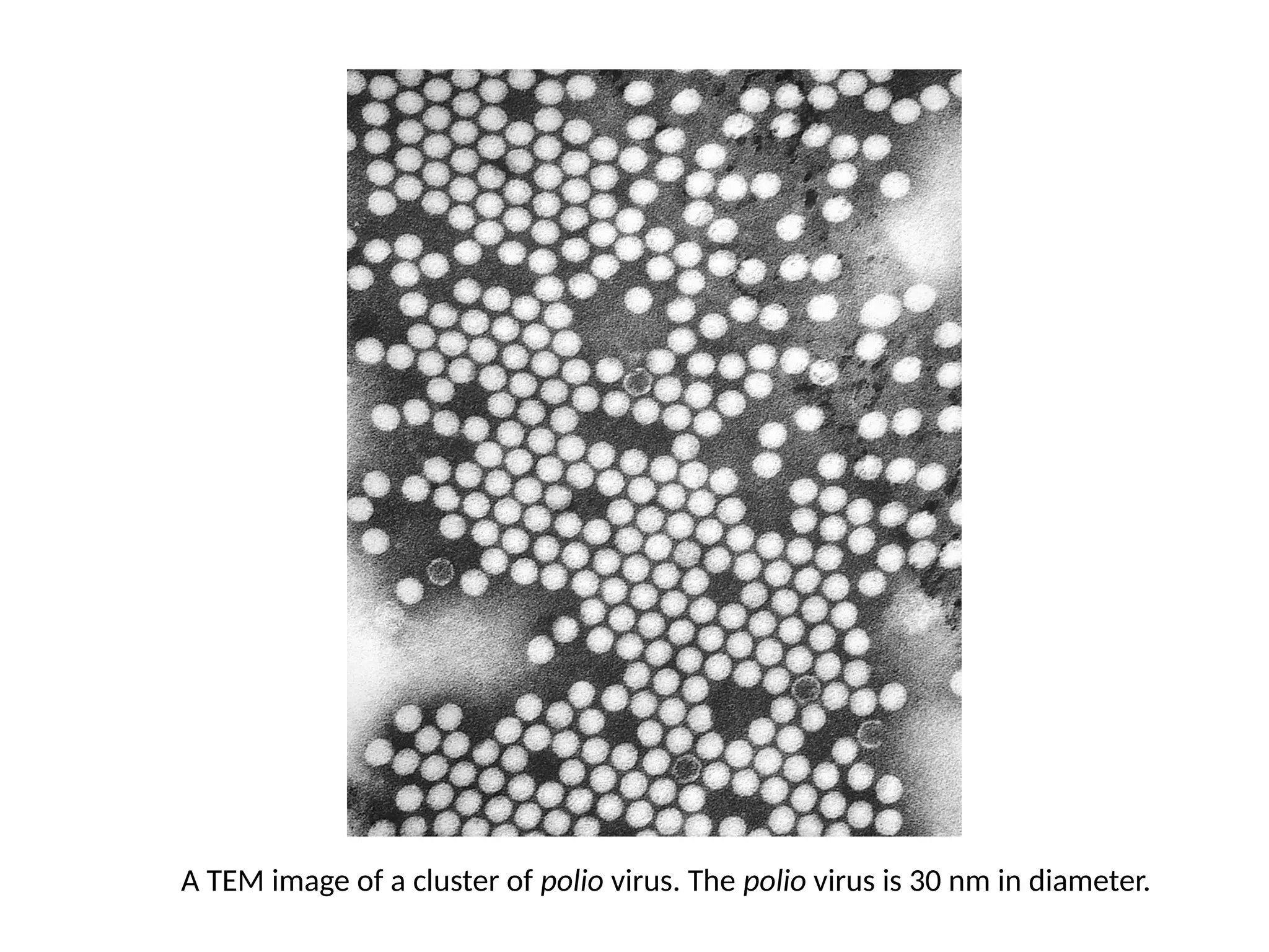
A TEM imageof a cluster of polio virus. The polio virus is 30 nm in diameter.
29.
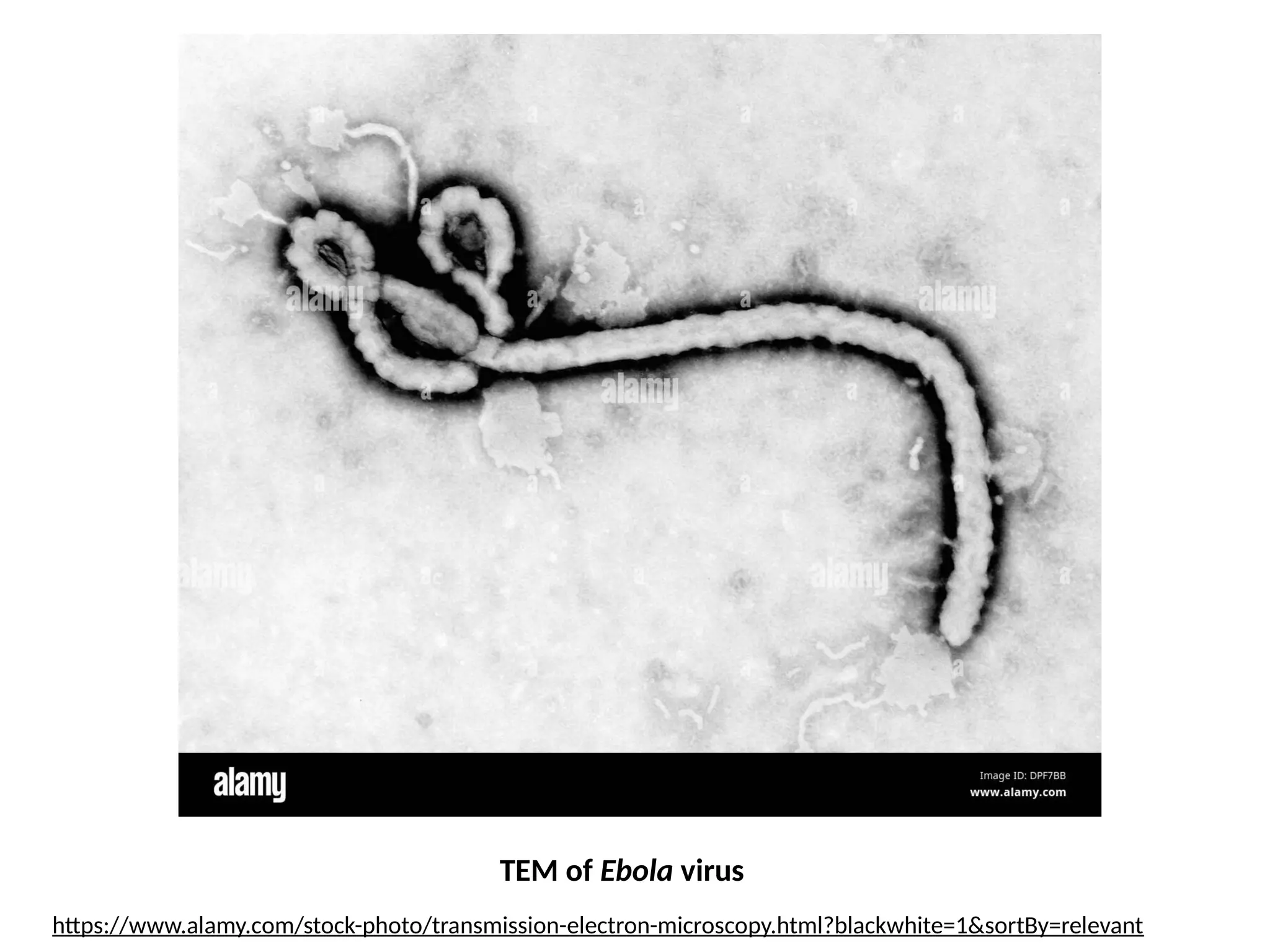
TEM of Ebolavirus
https://www.alamy.com/stock-photo/transmission-electron-microscopy.html?blackwhite=1&sortBy=relevant
30.
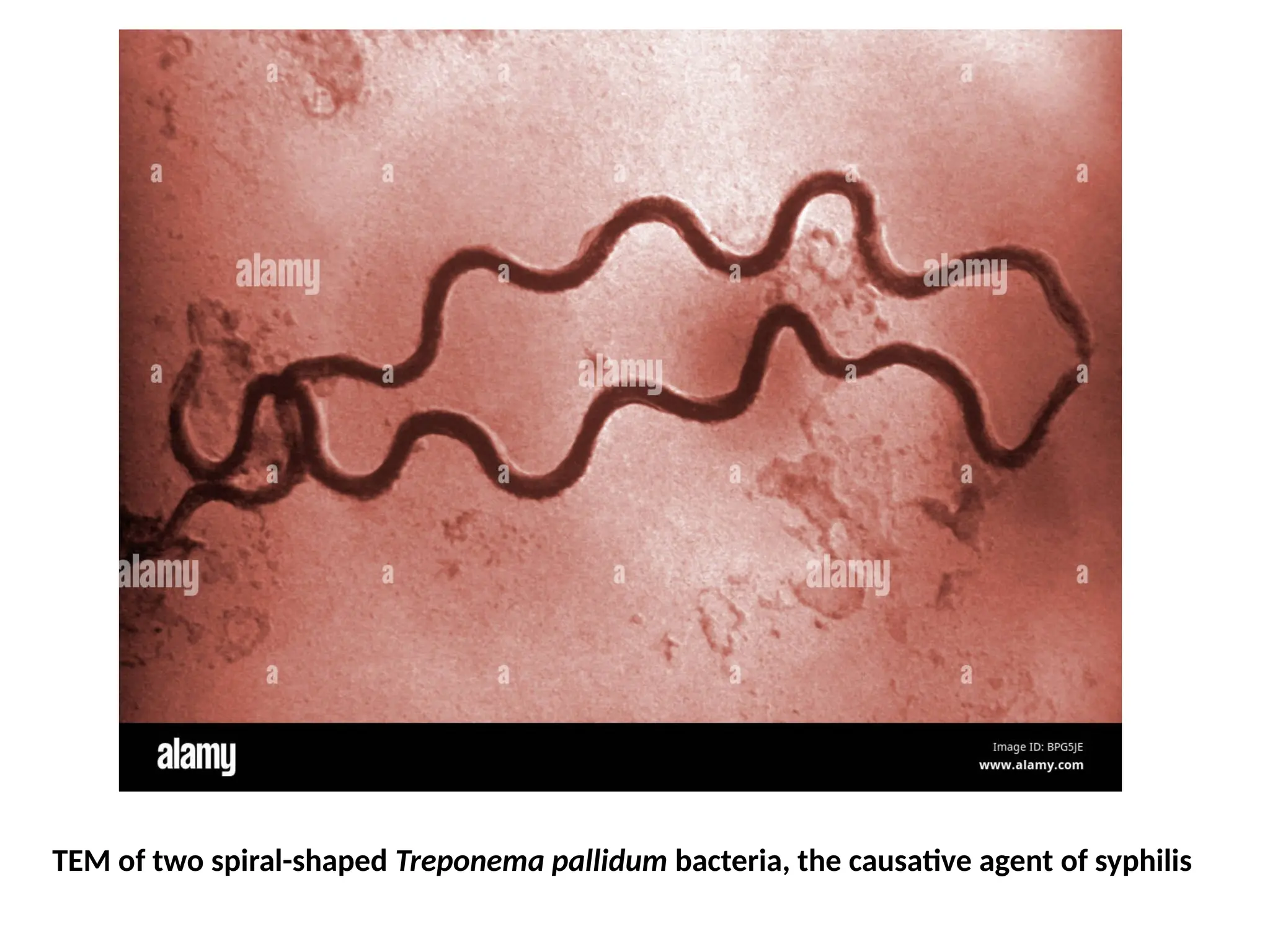
TEM of twospiral-shaped Treponema pallidum bacteria, the causative agent of syphilis
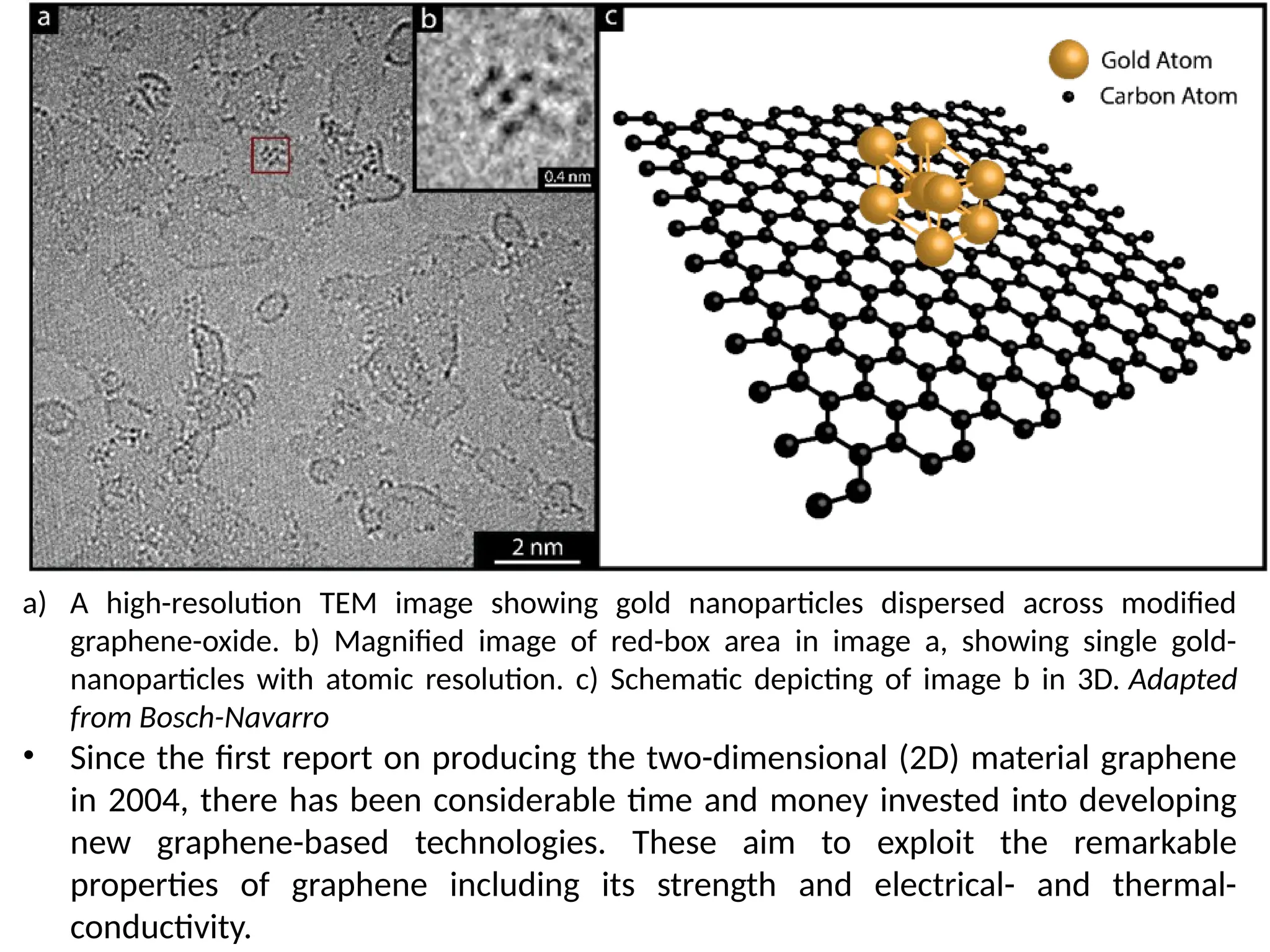
a) A high-resolutionTEM image showing gold nanoparticles dispersed across modified
graphene-oxide. b) Magnified image of red-box area in image a, showing single gold-
nanoparticles with atomic resolution. c) Schematic depicting of image b in 3D. Adapted
from Bosch-Navarro
• Since the first report on producing the two-dimensional (2D) material graphene
in 2004, there has been considerable time and money invested into developing
new graphene-based technologies. These aim to exploit the remarkable
properties of graphene including its strength and electrical- and thermal-
conductivity.
34.
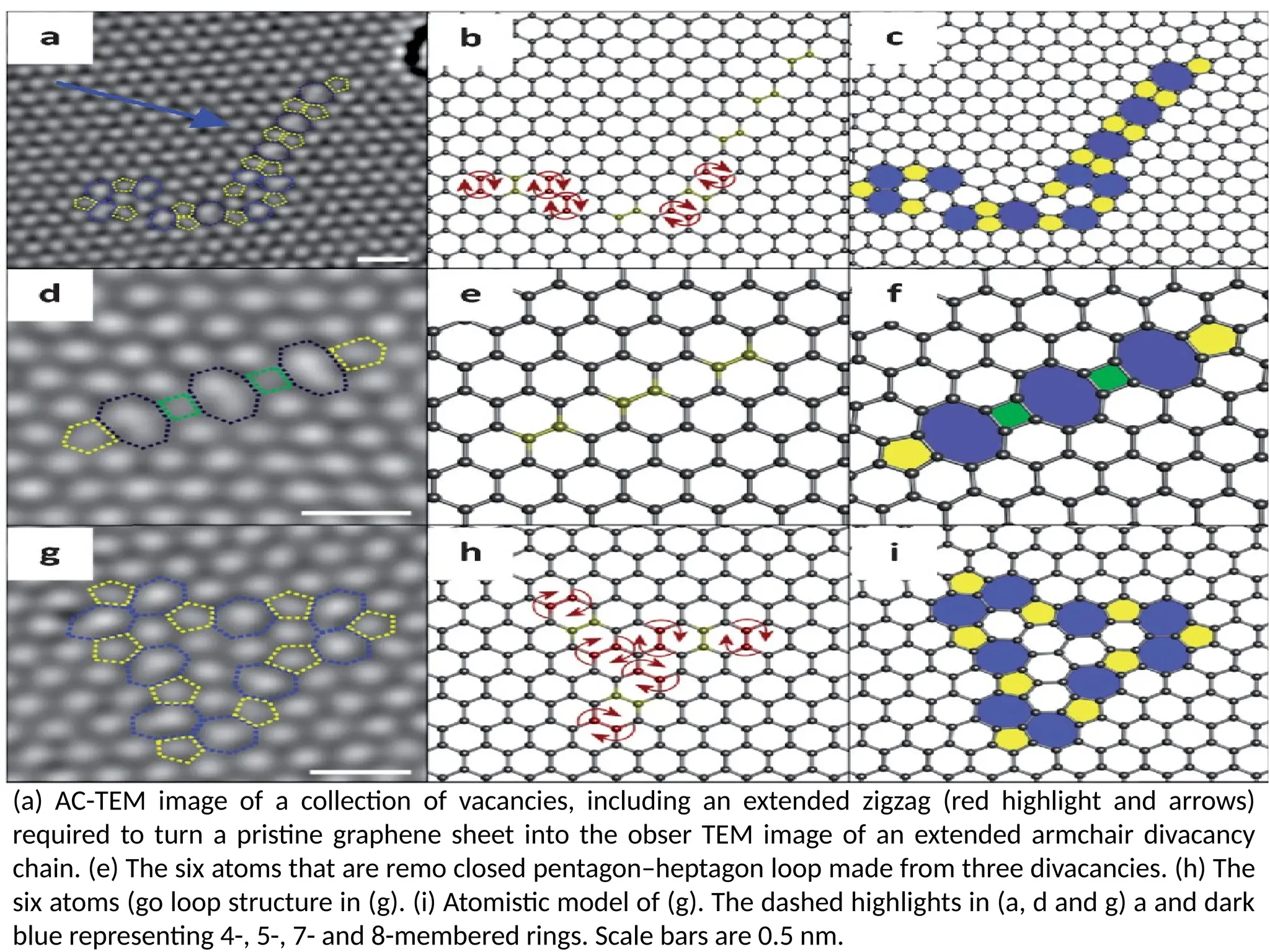
(a) AC-TEM imageof a collection of vacancies, including an extended zigzag (red highlight and arrows)
required to turn a pristine graphene sheet into the obser TEM image of an extended armchair divacancy
chain. (e) The six atoms that are remo closed pentagon–heptagon loop made from three divacancies. (h) The
six atoms (go loop structure in (g). (i) Atomistic model of (g). The dashed highlights in (a, d and g) a and dark
blue representing 4-, 5-, 7- and 8-membered rings. Scale bars are 0.5 nm.
35.
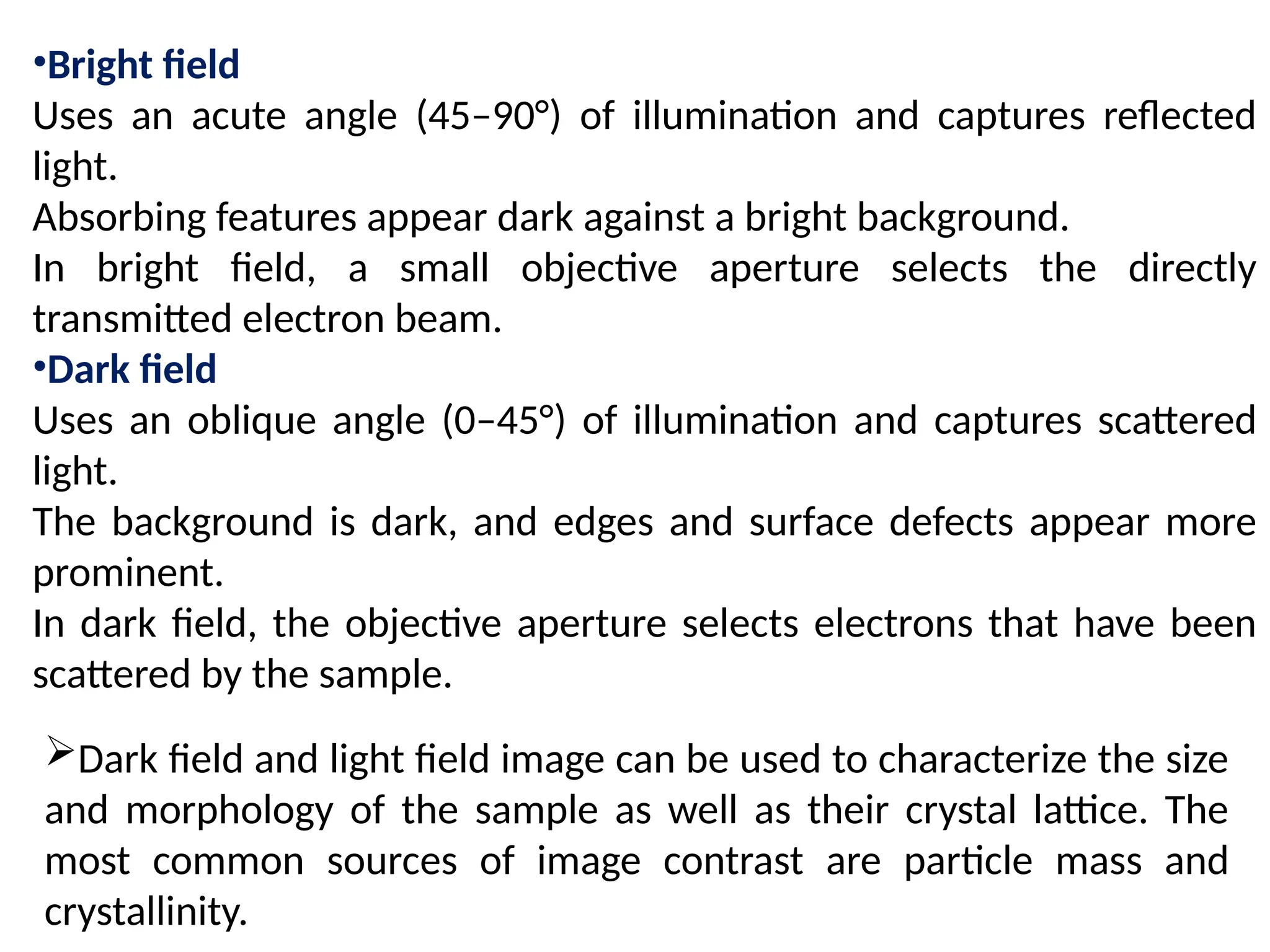
•Bright field
Uses anacute angle (45–90°) of illumination and captures reflected
light.
Absorbing features appear dark against a bright background.
In bright field, a small objective aperture selects the directly
transmitted electron beam.
•Dark field
Uses an oblique angle (0–45°) of illumination and captures scattered
light.
The background is dark, and edges and surface defects appear more
prominent.
In dark field, the objective aperture selects electrons that have been
scattered by the sample.
Dark field and light field image can be used to characterize the size
and morphology of the sample as well as their crystal lattice. The
most common sources of image contrast are particle mass and
crystallinity.
36.
Differences between brightfield and dark field
The main difference between bright field and dark field is the angle at
which the illuminating beam hits the sample and the type of light that is
captured.
Another main difference between the bright field and dark field mode is
which electron populations are used to construct the TEM image.
The darker an area is in a TEM image, the heavier the atom at that
location.
Heavier atoms scatter electrons more intensely than lighter atoms.
Hence, in bright field mode, the regions with heavier atoms are darker,
while in dark field mode these regions are brighter.
In biological and polymeric samples with low atomic number, staining
can help enhance the image contrast.
Bright field is the more commonly used lighting technique whereas dark
field is advantageous when imaging things such as reflective surfaces
and edge inspections.
Samples that are more crystalline are also more strongly diffracted and
will appear darker in bright field mode, and brighter in dark field mode.
37.
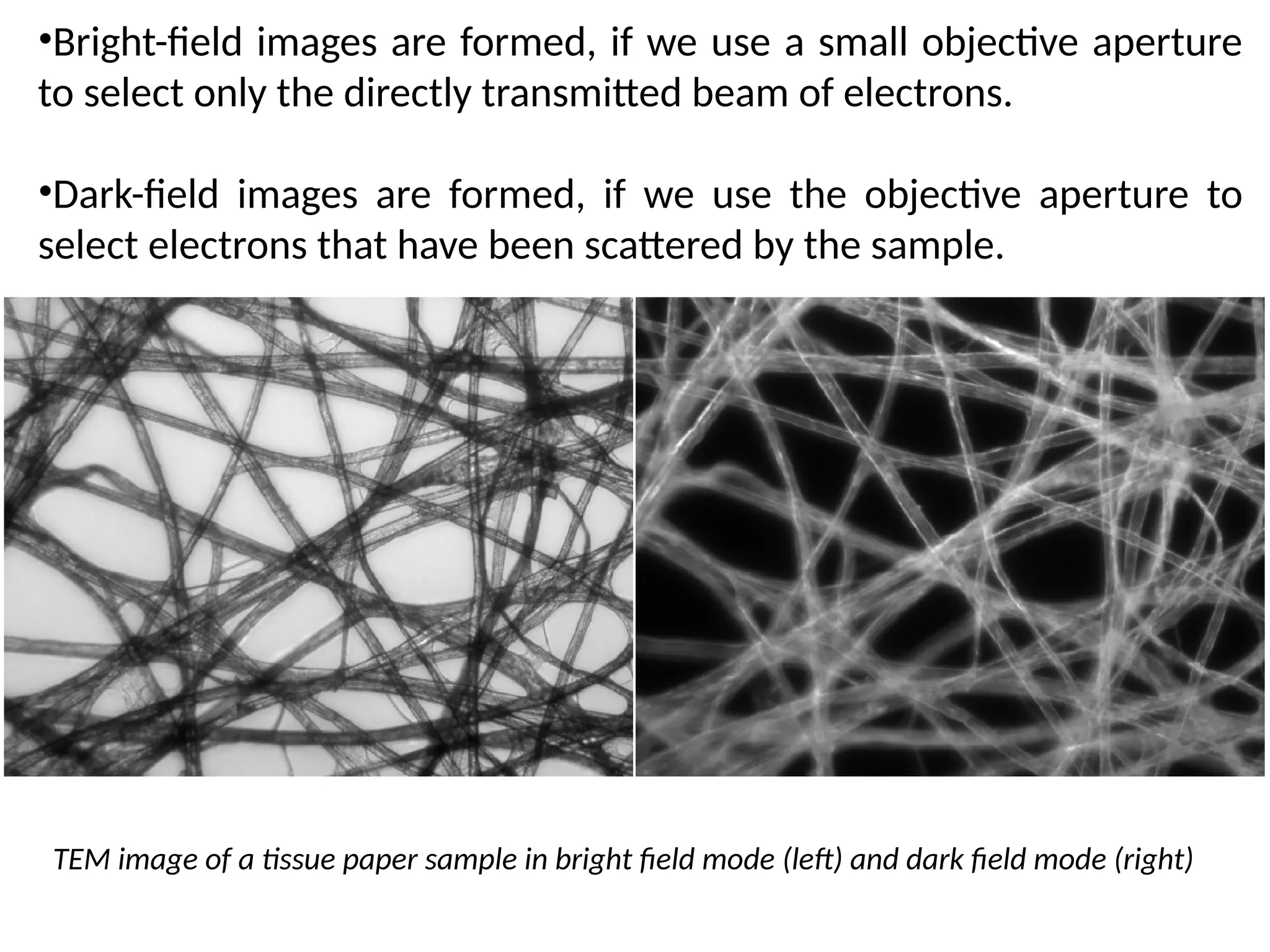
TEM image ofa tissue paper sample in bright field mode (left) and dark field mode (right)
•Bright-field images are formed, if we use a small objective aperture
to select only the directly transmitted beam of electrons.
•Dark-field images are formed, if we use the objective aperture to
select electrons that have been scattered by the sample.
41.
In a TEM,diffraction and image formation occur in two stages:
Diffraction
The electron beam scatters off the specimen, and the scattered
electrons that travel in the same direction are focused in the back
focal plane of the objective lens to form a diffraction pattern.
•Diffraction patterns occur due to elastic interferrence (diffraction) of
the electron beam as it passes through crystalline specimens.
•This can be most easily understood by remembering that the
electron beam has wave-like properties.
•The ability of the TEM to form these diffraction patterns is unique to
this kind of instrument, but does require advanced understanding of
the path of the electron beam within the instrument, and also a
strong understanding of crystallography.
https://upload.wikimedia.org/wikipedia/commons/transcoded/6/6b/Transmission_Electron
_Microscope_operating_principle.ogv/Transmission_Electron_Microscope_operating_princi
ple.ogv.1080p.vp9.webm
42.
Selected Area Diffraction(SAD), also known as Selected
Area Electron Diffraction (SAED), is a crucial technique used
in Transmission Electron Microscopy (TEM). This method
allows researchers to obtain diffraction patterns from a
specific area of interest within a sample, such as a single
grain in a polycrystalline material .
How SAD Works?
In SAD, a parallel electron beam is directed onto the
specimen, and a small aperture is used to isolate a particular
region. This ensures that only the selected area contributes
to the diffraction pattern, which is essential for analyzing the
crystallographic structure of materials. The technique is
particularly useful for determining whether a specimen is
single crystal, polycrystalline, or amorphous, and for
identifying its crystallographic structure
43.
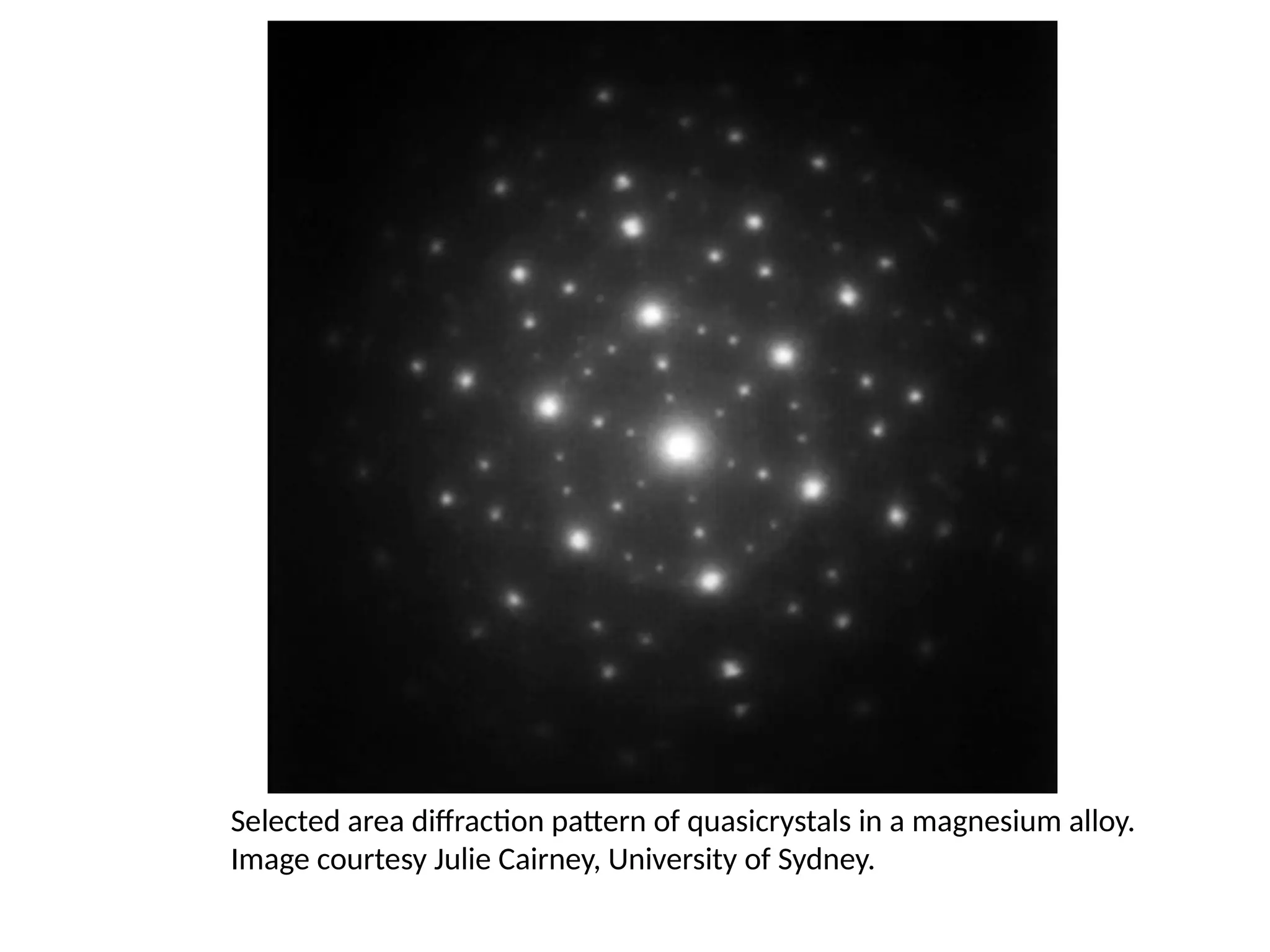
Selected area diffractionpattern of quasicrystals in a magnesium alloy.
Image courtesy Julie Cairney, University of Sydney.
44.
Applications of SAD
SADis widely employed in materials science for qualitative
analysis of crystal structures. It provides valuable information
about the orientation and phase of materials, which is critical
for understanding their properties and behaviors. The
technique is also beneficial in research fields such as
nanotechnology and semiconductor fabrication, where
precise structural information is necessary.
45.
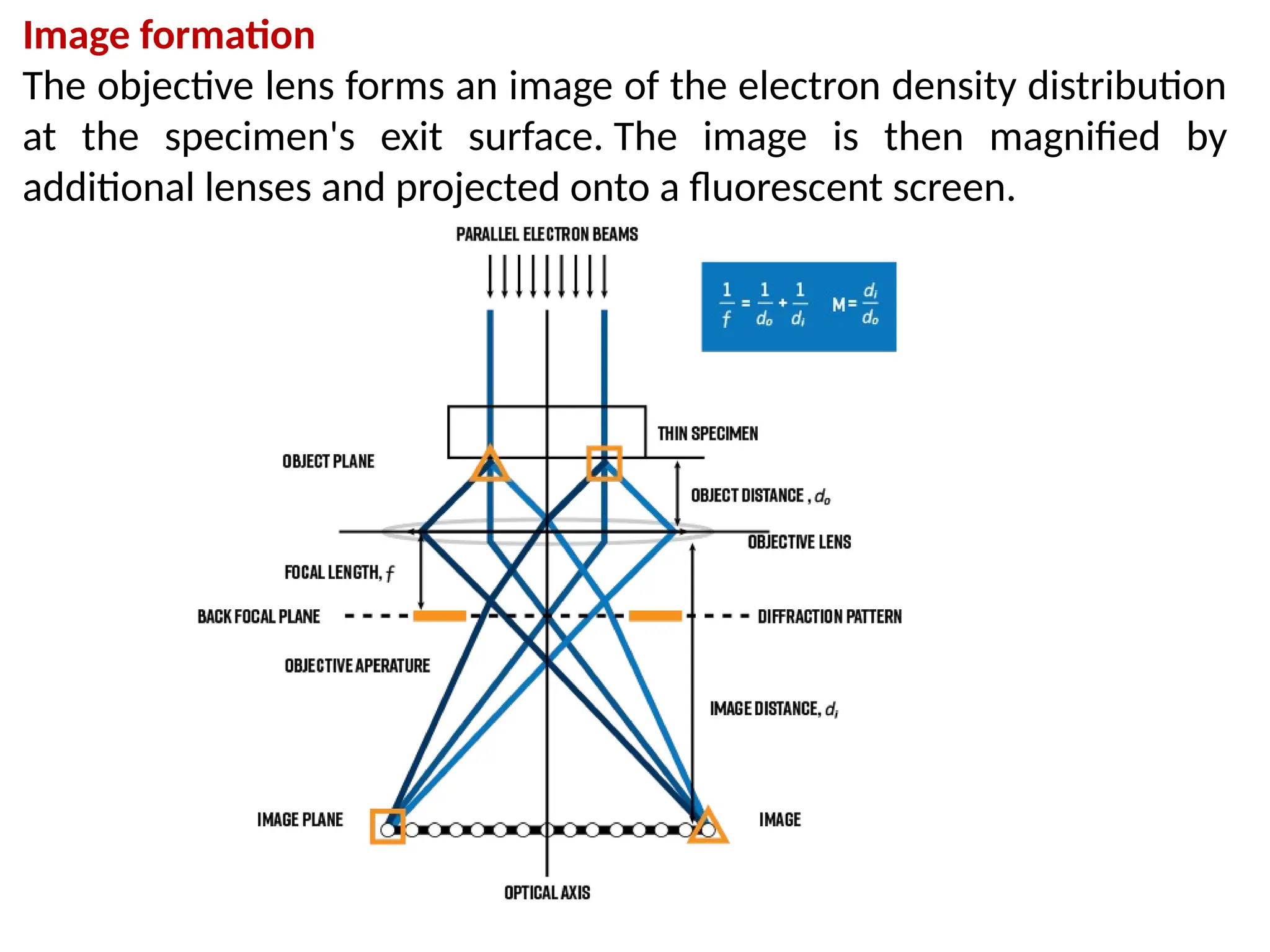
Image formation
The objectivelens forms an image of the electron density distribution
at the specimen's exit surface. The image is then magnified by
additional lenses and projected onto a fluorescent screen.
47.
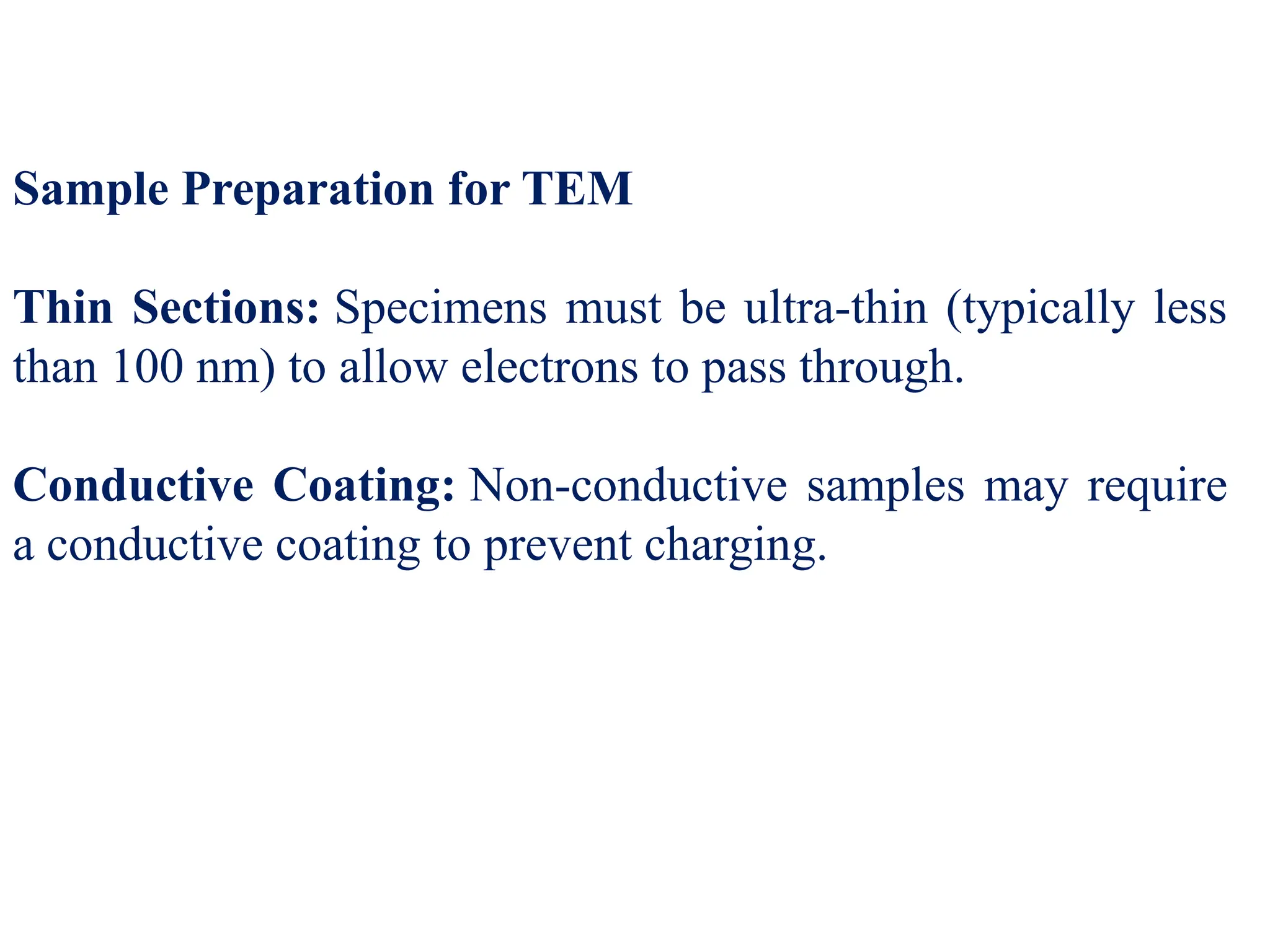
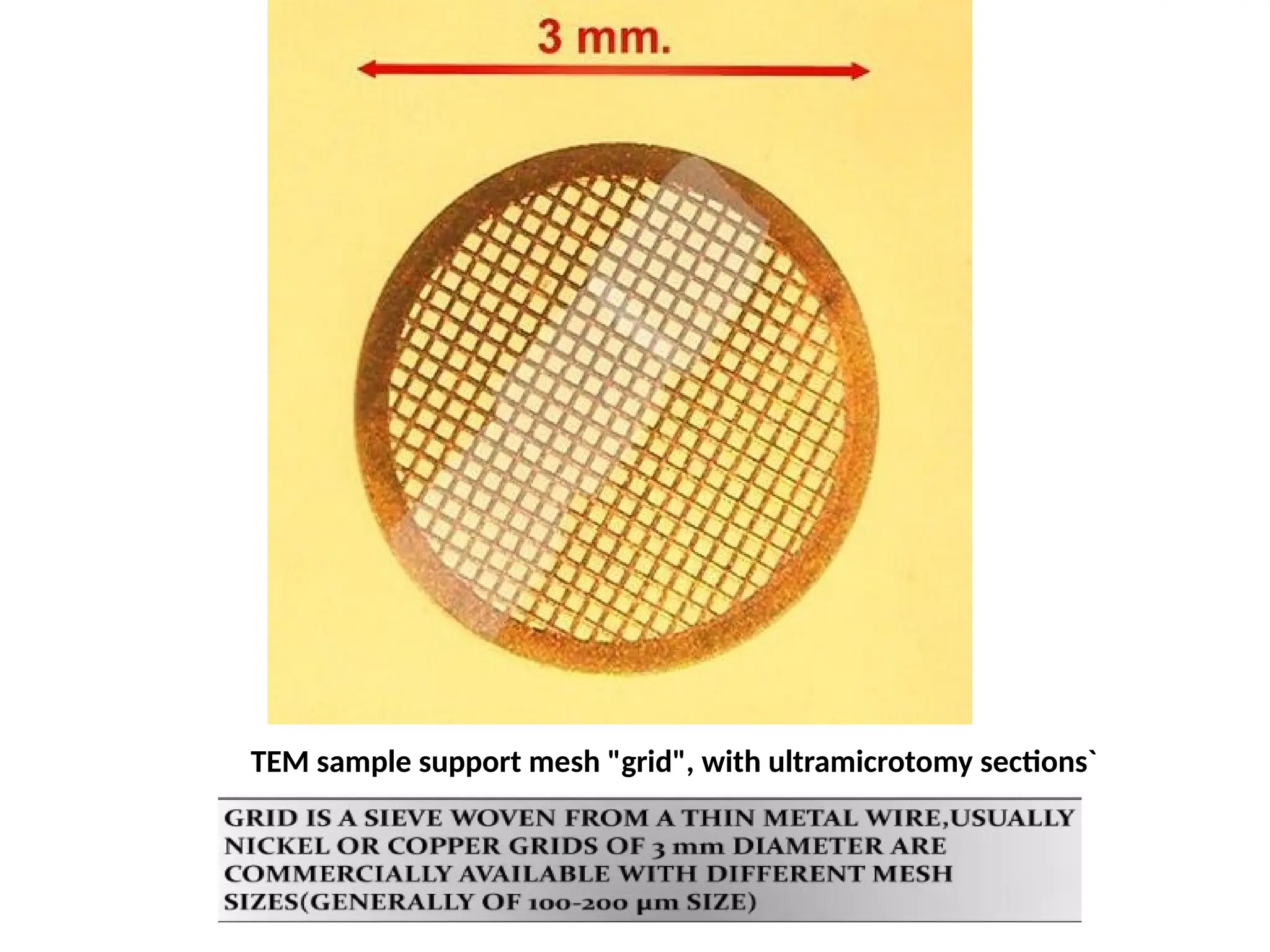
Sample Preparation forTEM
Thin Sections: Specimens must be ultra-thin (typically less
than 100 nm) to allow electrons to pass through.
Conductive Coating: Non-conductive samples may require
a conductive coating to prevent charging.
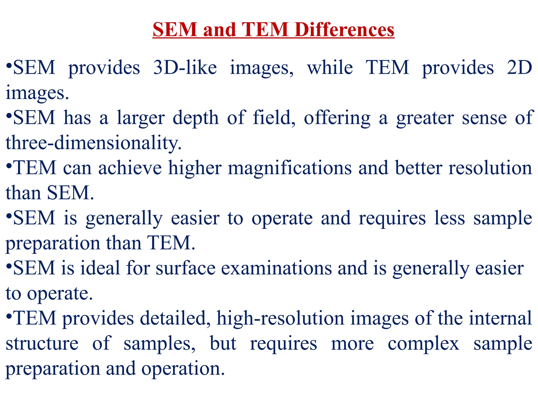
SEM and TEMDifferences
•SEM provides 3D-like images, while TEM provides 2D
images.
•SEM has a larger depth of field, offering a greater sense of
three-dimensionality.
•TEM can achieve higher magnifications and better resolution
than SEM.
•SEM is generally easier to operate and requires less sample
preparation than TEM.
•SEM is ideal for surface examinations and is generally easier
to operate.
•TEM provides detailed, high-resolution images of the internal
structure of samples, but requires more complex sample
preparation and operation.
54.
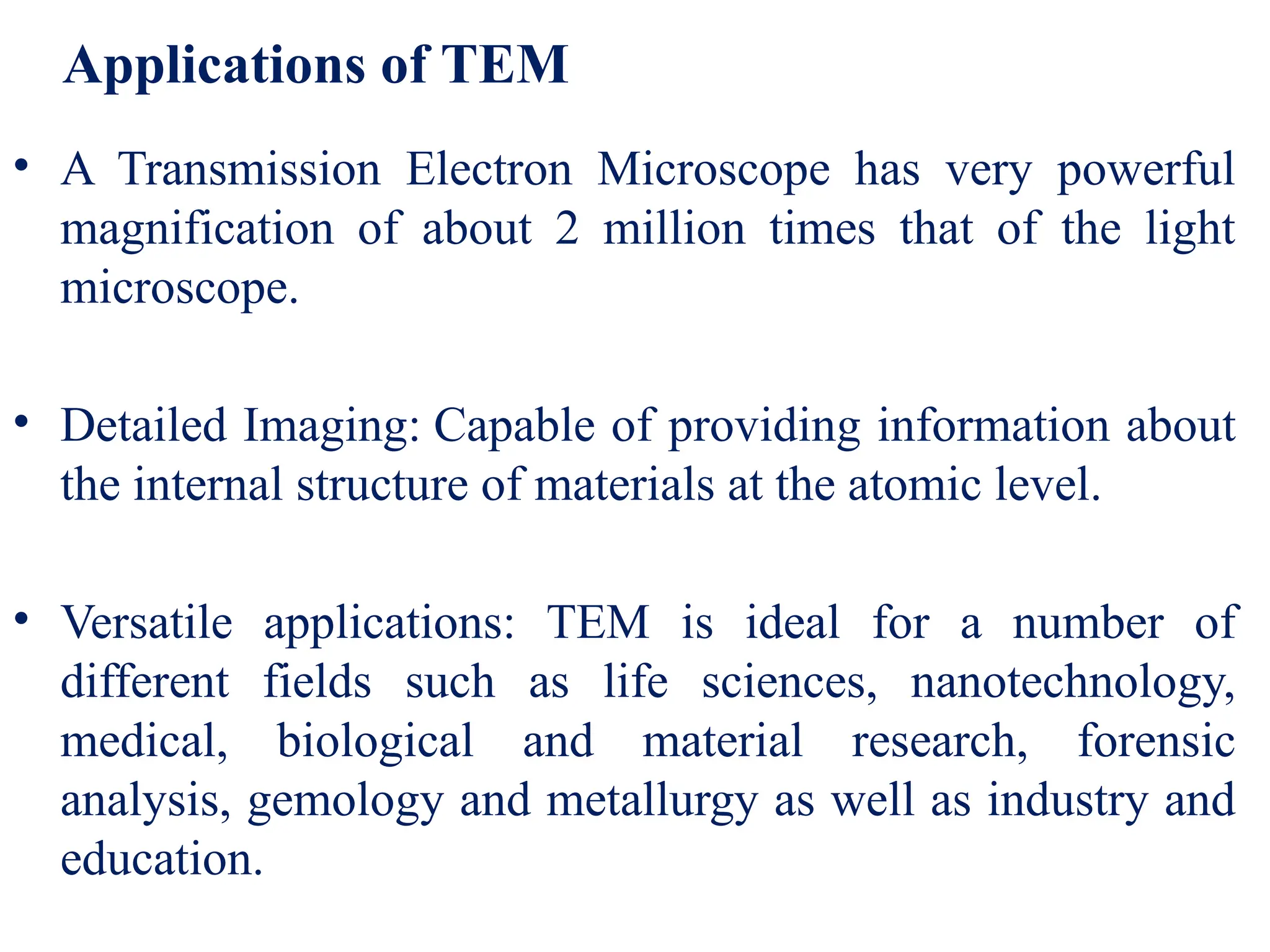
Applications of TEM
•A Transmission Electron Microscope has very powerful
magnification of about 2 million times that of the light
microscope.
• Detailed Imaging: Capable of providing information about
the internal structure of materials at the atomic level.
• Versatile applications: TEM is ideal for a number of
different fields such as life sciences, nanotechnology,
medical, biological and material research, forensic
analysis, gemology and metallurgy as well as industry and
education.
55.
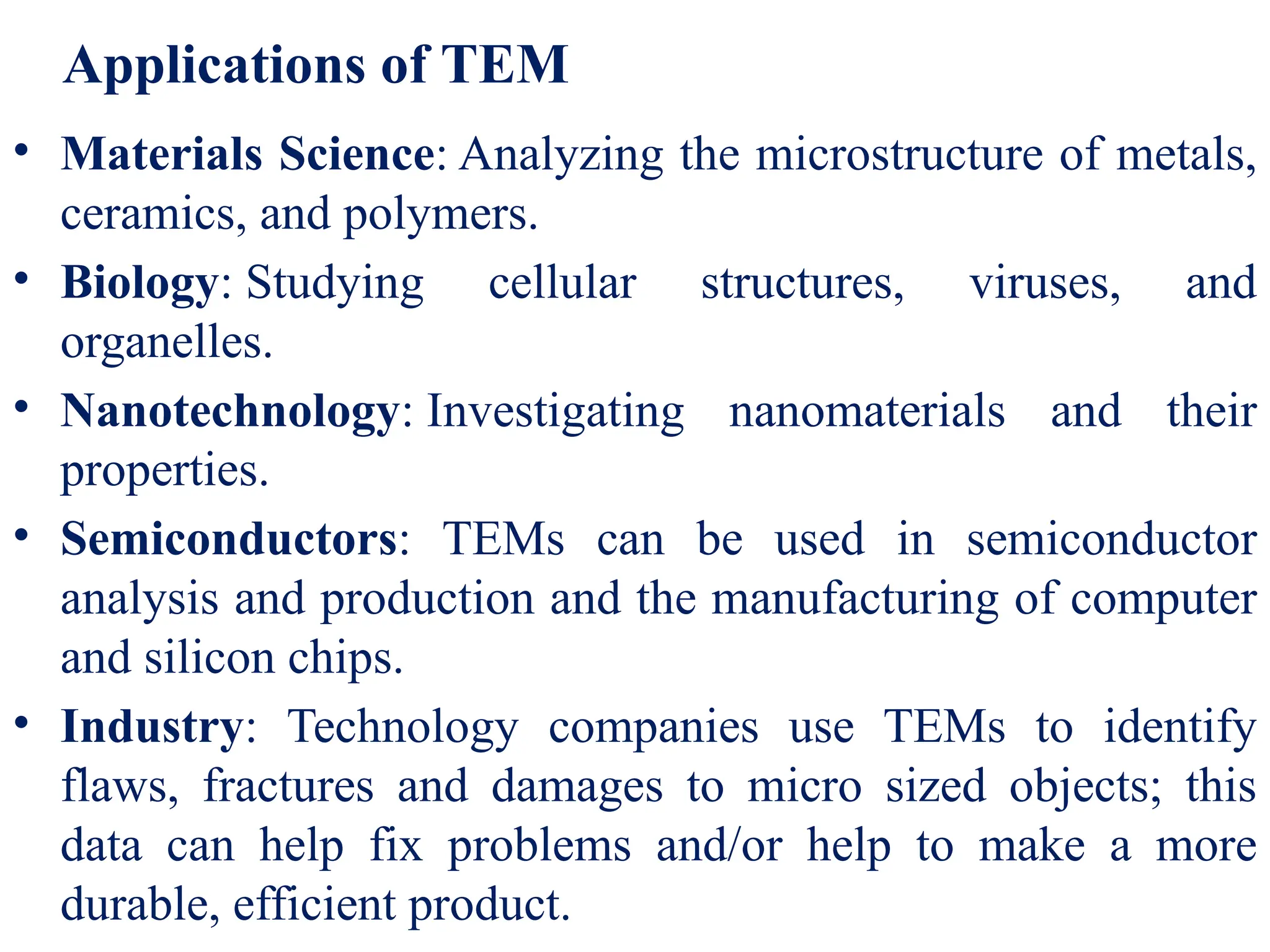
• Materials Science:Analyzing the microstructure of metals,
ceramics, and polymers.
• Biology: Studying cellular structures, viruses, and
organelles.
• Nanotechnology: Investigating nanomaterials and their
properties.
• Semiconductors: TEMs can be used in semiconductor
analysis and production and the manufacturing of computer
and silicon chips.
• Industry: Technology companies use TEMs to identify
flaws, fractures and damages to micro sized objects; this
data can help fix problems and/or help to make a more
durable, efficient product.
Applications of TEM
56.
Advantages of TEM
•Theadvantages of the TEM include that they are very powerful
microscopes with high magnification resolution.
•They have a wide range of applications and provide information on
elements and compound structures.
•The images are high quality and detailed with chemical Information
with analytical attachments.
•TEM can reveal stunning detail at the atomic scale by magnifying
nanometer structures up to 50 million times.
57.
Disadvantages of TEM
•TEMs are large and very expensive
• Laborious sample preparation
• Operation and analysis requires special training
• Samples are limited to those that are electron transparent, able to
tolerate the vacuum chamber and small enough to fit in the chamber
• TEMs require special housing and maintenance
• Images are black and white.
• It is important to mention that most of the chemicals used in EM are
dangerous. Investigator must be aware of potential hazards such as
fire, chemical, electrical and physical associated with these items.
• The disadvantage of the TEM is that they are very large and
expensive setups, which need tedious sample preparation.
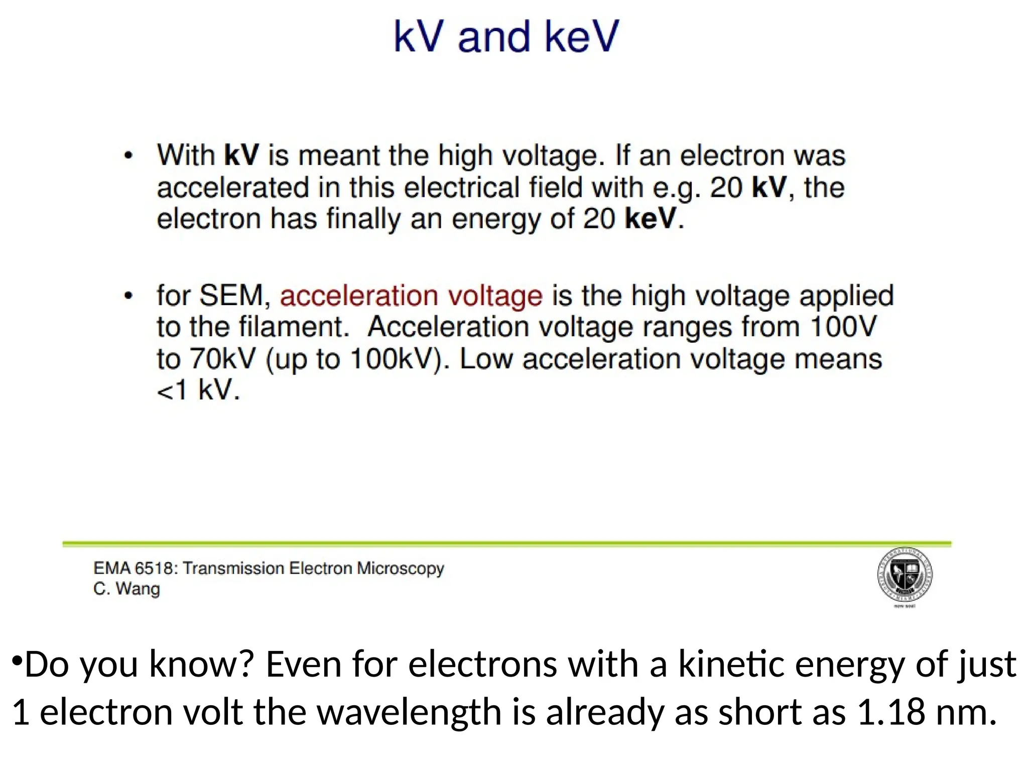
•Do you know?Even for electrons with a kinetic energy of just
1 electron volt the wavelength is already as short as 1.18 nm.
62.
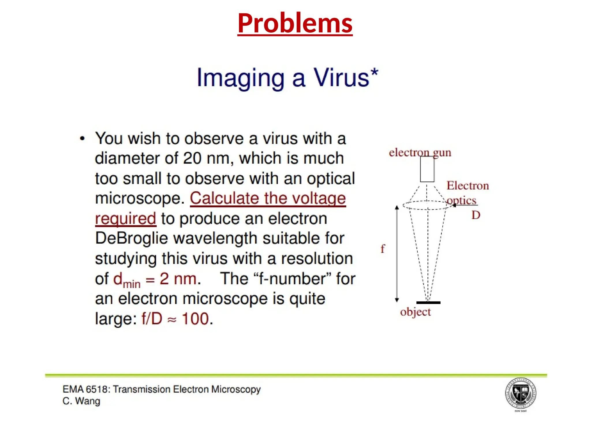
Q: A basicsimple magnification microscope is being used in light with a wavelength of
555 nm. It has an objective lens with a diameter of 5.00 cm. This is the aperture. The
specimen is 15.0 cm away from the objective lens. What is the resolution in meters?
In micrometers which are also called microns? The width of a human hair is 20
microns. Will this microscope be able to resolve human hair?
Ans: Microscopes: x=1.22 λ (d/D) = 2.01×10⁻⁶
m = 2.03 microns which is much less
than the 20 micron hair so it will be able to resolve it.
Q: Covid-19 virus has a size of 88 nm. An optical compound microscope such as that
found in most first year college labs has an objective lens with a diameter of 2.0 cm
and the virus is on a slide that is being viewed from a distance of 0.50 cm. If it is being
viewed in light with a wavelength of 555 nm. a) what is the resolution in a) metres b)
nanometres of this microscope? Can you see the virus using this microscope? Yes or
no?
Ans: 1.7 x10⁻⁷
m = 170 nm No, the virus cannot be seen as it is smaller than the
resolution of this microscope.
Q: What wavelength of electromagnetic radiation do you need to view the a Covid-19
virus particle with a size of 82 nanometres? Assume the diameter of the objective lens
is 2.0 mm and it is being viewed from 3.0 cm away.
Ans: 4.5 x10⁻⁹
m = 4.5 nm much smaller than visible light. This is ultraviolet
electromagnetic radiation.