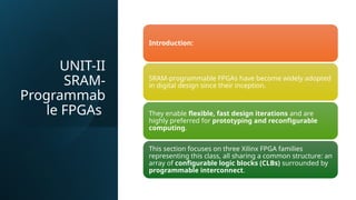
UNIT-II
SRAM-
Programmab
le FPGAs
Introduction:
SRAM-programmable FPGAshave become widely adopted
in digital design since their inception.
They enable flexible, fast design iterations and are
highly preferred for prototyping and reconfigurable
computing.
This section focuses on three Xilinx FPGA families
representing this class, all sharing a common structure: an
array of configurable logic blocks (CLBs) surrounded by
programmable interconnect.
2.
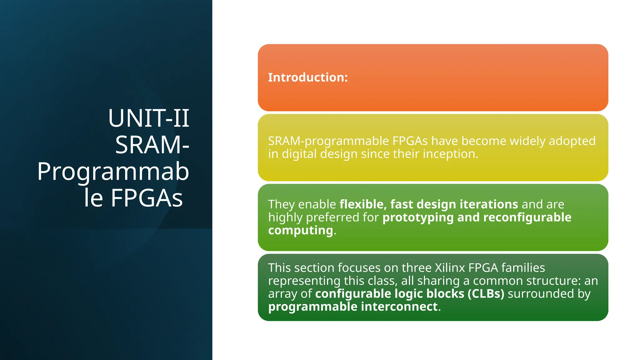
Programming Technology
SRAM Configuration:
FPGAsare programmed
using an external
source that loads data
into distributed
configuration memory
cells.
These cells control both
logic and interconnect
paths.
Unlike traditional RAM,
these cells do not
require high-speed
read/write access
because programming
occurs only once per
application.
Stability and density are
emphasized over speed.
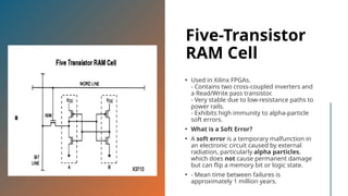
Five-Transistor
RAM Cell
• Usedin Xilinx FPGAs.
- Contains two cross-coupled inverters and
a Read/Write pass transistor.
- Very stable due to low-resistance paths to
power rails.
- Exhibits high immunity to alpha-particle
soft errors.
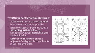
• What is a Soft Error?
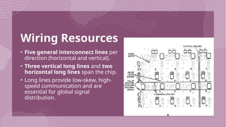
• A soft error is a temporary malfunction in
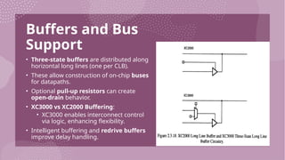
an electronic circuit caused by external
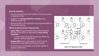
radiation, particularly alpha particles,
which does not cause permanent damage
but can flip a memory bit or logic state.
• - Mean time between failures is
approximately 1 million years.
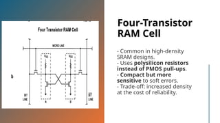
5.
Four-Transistor
RAM Cell
- Commonin high-density
SRAM designs.
- Uses polysilicon resistors
instead of PMOS pull-ups.
- Compact but more
sensitive to soft errors.
- Trade-off: increased density
at the cost of reliability.
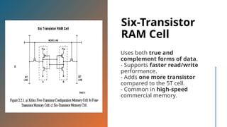
6.
Six-Transistor
RAM Cell
Uses bothtrue and
complement forms of data.
- Supports faster read/write
performance.
- Adds one more transistor
compared to the 5T cell.
- Common in high-speed
commercial memory.
7.
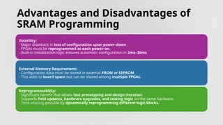
Advantages and Disadvantagesof
SRAM Programming
Volatility:
- Major drawback is loss of configuration upon power-down.
- FPGAs must be reprogrammed at each power-on.
- Built-in initialization logic ensures automatic configuration in 2ms–30ms.
External Memory Requirement:
- Configuration data must be stored in external PROM or EEPROM.
- This adds to board space but can be shared among multiple FPGAs.
Reprogrammability:
- Significant benefit that allows fast prototyping and design iteration.
- Supports field updates, hardware upgrades, and testing logic on the same hardware.
- Time-sharing possible by dynamically reprogramming different logic blocks.
8.
Advantages
and
Disadvantag
es of SRAM
Programmin
g
•Testing and Quality:
- SRAM FPGAs are fully testable before
shipping.
- Supports detection of faults like stuck-at,
stuck-open, and bridging faults.
- Devices can be speed-binned to ensure
performance classification.
• speed binning is a post-manufacturing
testing process in which integrated
circuits (ICs)—such as CPUs, GPUs,
FPGAs, or memory chips—are classified
based on how fast they can operate
reliably.
Programming Yield:
- Always 100% as there's no physical
programming process that could damage
the chip.
- No insertion/removal cycles as in
EPROM/antifuse types.
9.
Advantages
and
Disadvantag
es of SRAM
Programmin
g
•Process Compatibility:
- Uses standard CMOS technology
similar to ASICs and commercial
memories.
- Benefits from the latest advances
in process scaling for speed and
density.
Low Power:
- Logic implemented using static
CMOS gates.
- Consumes very little power and
has zero standby current.
- Preferred over EPLDs that
consume more due to sense
amplifiers and passive pull-ups.
10.
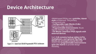
Device Architecture
•SRAM-based FPGAsuse a grid-like, island-
style architecture. The primary
components are:
- Configurable Logic Blocks (CLBs):
Implement logic functions.
- Programmable Interconnects: Route
signals between logic blocks.
- I/O Blocks: Interface FPGA signals with
external devices.
Each CLB contains lookup tables (LUTs),
multiplexers, and optional flip-flops. I/O
blocks are arranged around the CLB
matrix and programmable interconnects
span the matrix to provide design
flexibility.
11.
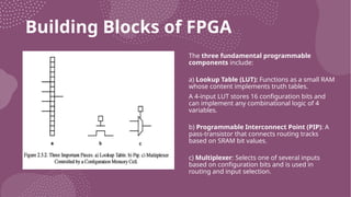
Building Blocks ofFPGA
The three fundamental programmable
components include:
a) Lookup Table (LUT): Functions as a small RAM
whose content implements truth tables.
A 4-input LUT stores 16 configuration bits and
can implement any combinational logic of 4
variables.
b) Programmable Interconnect Point (PIP): A
pass-transistor that connects routing tracks
based on SRAM bit values.
c) Multiplexer: Selects one of several inputs
based on configuration bits and is used in
routing and input selection.
12.
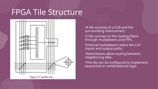
FPGA Tile Structure
•Atile consists of a CLB and the
surrounding interconnect.
•CLBs connect to the routing fabric
through multiplexers and PIPs.
•Internal multiplexers select the LUT
inputs and output paths.
•Switchboxes allow routing between
neighboring tiles.
•The tile can be configured to implement
sequential or combinational logic.
13.
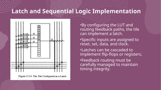
Latch and SequentialLogic Implementation
•By configuring the LUT and
routing feedback paths, the tile
can implement a latch.
•Specific inputs are assigned to
reset, set, data, and clock.
•Latches can be cascaded to
implement flip-flops or registers.
•Feedback routing must be
carefully managed to maintain
timing integrity.
14.
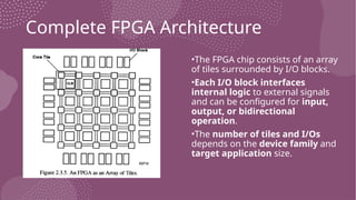
Complete FPGA Architecture
•TheFPGA chip consists of an array
of tiles surrounded by I/O blocks.
•Each I/O block interfaces
internal logic to external signals
and can be configured for input,
output, or bidirectional
operation.
•The number of tiles and I/Os
depends on the device family and
target application size.
15.
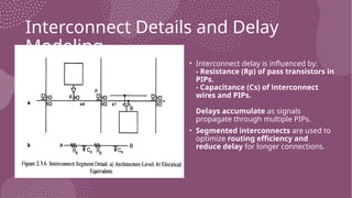
Interconnect Details andDelay
Modeling
• Interconnect delay is influenced by:
- Resistance (Rp) of pass transistors in
PIPs.
- Capacitance (Cs) of interconnect
wires and PIPs.
Delays accumulate as signals
propagate through multiple PIPs.
• Segmented interconnects are used to
optimize routing efficiency and
reduce delay for longer connections.
16.
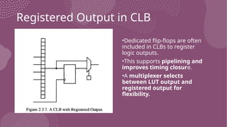
Registered Output inCLB
•Dedicated flip-flops are often
included in CLBs to register
logic outputs.
•This supports pipelining and
improves timing closure.
•A multiplexer selects
between LUT output and
registered output for
flexibility.
17.
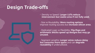
Design Trade-offs
- Densityvs Speed: Larger LUTs reduce
interconnect but waste area if not fully used.
- Size vs Routability: More routing options
improve routing success but increase silicon area.
- Dedicated Logic vs Flexibility: Flip-flops and
arithmetic blocks speed up designs but may go
unused.
- Segment Lengths: Longer wires reduce delay
but consume more space and can degrade
routability if underutilized.
18.
Capacity
Estimation and
Logic Mapping
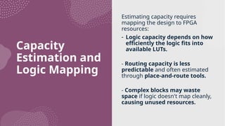
Estimatingcapacity requires
mapping the design to FPGA
resources:
- Logic capacity depends on how
efficiently the logic fits into
available LUTs.
- Routing capacity is less
predictable and often estimated
through place-and-route tools.
- Complex blocks may waste
space if logic doesn't map cleanly,
causing unused resources.
19.
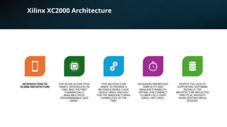
Xilinx XC2000 Architecture
INTRODUCTIONTO
XC2000 ARCHITECTURE
THE XILINX XC2000 FPGA
FAMILY, INTRODUCED IN
1985, WAS THE FIRST
COMMERCIALLY
AVAILABLE FIELD-
PROGRAMMABLE GATE
ARRAY.
THIS ARCHITECTURE
AIMED TO PROVIDE A
RECONFIGURABLE LOGIC
DEVICE SMALL ENOUGH
FOR THE MANUFACTURING
CAPABILITIES OF THE
TIME.
DESIGNERS PRIORITIZED
SIMPLICITY AND
MANUFACTURABILITY,
OPTING FOR COMPACT,
SLOWER CELLS OVER
LARGE, FAST ONES.
DESPITE THE LACK OF
SUPPORTING SOFTWARE
INITIALLY, THE
ARCHITECTURE REFLECTED
PRACTICAL INSIGHTS
FROM EXISTING MPGA
DESIGNS.
20.
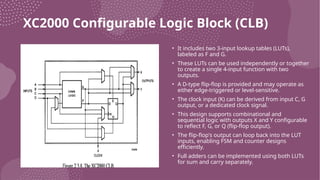
XC2000 Configurable LogicBlock (CLB)
• It includes two 3-input lookup tables (LUTs),
labeled as F and G.
• These LUTs can be used independently or together
to create a single 4-input function with two
outputs.
• A D-type flip-flop is provided and may operate as
either edge-triggered or level-sensitive.
• The clock input (K) can be derived from input C, G
output, or a dedicated clock signal.
• This design supports combinational and
sequential logic with outputs X and Y configurable
to reflect F, G, or Q (flip-flop output).
• The flip-flop's output can loop back into the LUT
inputs, enabling FSM and counter designs
efficiently.
• Full adders can be implemented using both LUTs
for sum and carry separately.
21.
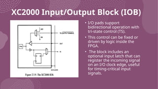
XC2000 Input/Output Block(IOB)
• I/O pads support
bidirectional operation with
tri-state control (TS).
• This control can be fixed or
driven by logic inside the
FPGA.
• The block includes an
optional input latch that can
register the incoming signal
on an I/O clock edge, useful
for timing-critical input
signals.
22.
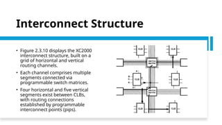
Interconnect Structure
• Figure2.3.10 displays the XC2000
interconnect structure, built on a
grid of horizontal and vertical
routing channels.
• Each channel comprises multiple
segments connected via
programmable switch matrices.
• Four horizontal and five vertical
segments exist between CLBs,
with routing connections
established by programmable
interconnect points (pips).
23.
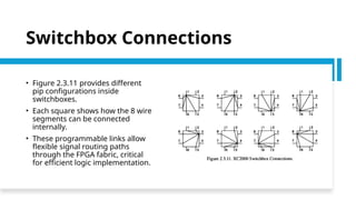
Switchbox Connections
• Figure2.3.11 provides different
pip configurations inside
switchboxes.
• Each square shows how the 8 wire
segments can be connected
internally.
• These programmable links allow
flexible signal routing paths
through the FPGA fabric, critical
for efficient logic implementation.
24.
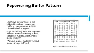
Repowering Buffer Pattern
•Asshown in Figure 2.3.12, the
XC2000 includes a repowering
buffer strategy where the die is
divided into nine regions.
•Signals crossing from one region to
another are boosted using buffers
to reduce RC delay and maintain
signal integrity.
•Within a region, local interconnect
signals are not buffered.
25.
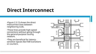
Direct Interconnect
•Figure 2.3.13shows the direct
interconnect lines between
neighboring CLBs.
•These lines provide high-speed
connections without going through
the general-purpose routing
network.
•They are beneficial for latency-
sensitive signals like FSM transitions
or counters.
26.
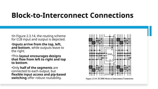
Block-to-Interconnect Connections
•In Figure2.3.14, the routing scheme
for CLB input and output is depicted.
•Inputs arrive from the top, left,
and bottom, while outputs leave to
the right.
•This layout encourages designs
that flow from left to right and top
to bottom.
•Only half of the segments are
connected to each output, but
flexible input access and pip-based
switching offer robust routability.
27.
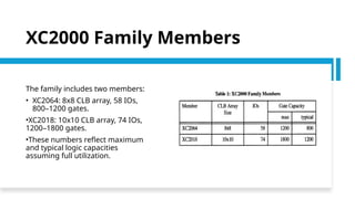
XC2000 Family Members
Thefamily includes two members:
• XC2064: 8x8 CLB array, 58 IOs,
800–1200 gates.
•XC2018: 10x10 CLB array, 74 IOs,
1200–1800 gates.
•These numbers reflect maximum
and typical logic capacities
assuming full utilization.
28.
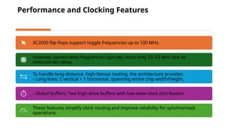
Performance and ClockingFeatures
XC2000 flip-flops support toggle frequencies up to 100 MHz.
However, system-level frequencies typically reach only 25–33 MHz due to
interconnect delay.
To handle long-distance, high-fanout routing, the architecture provides:
- Long lines: 2 vertical + 1 horizontal, spanning entire chip width/height.
- Global buffers: Two high-drive buffers with low-skew clock distribution.
These features simplify clock routing and improve reliability for synchronized
operations.
29.
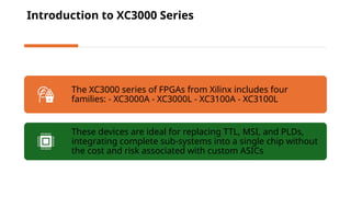
Introduction to XC3000Series
The XC3000 series of FPGAs from Xilinx includes four
families: - XC3000A - XC3000L - XC3100A - XC3100L
These devices are ideal for replacing TTL, MSI, and PLDs,
integrating complete sub-systems into a single chip without
the cost and risk associated with custom ASICs
30.
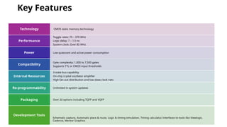
Key Features
CMOS staticmemory technology
Technology
Toggle rates: 70 – 370 MHz
Logic delay: 7 – 1.5 ns
System clock: Over 85 MHz
Performance
Low quiescent and active power consumption
Power
Gate complexity: 1,000 to 7,500 gates
Supports TTL or CMOS input thresholds
Compatibility
3-state bus capability
On-chip crystal oscillator amplifier
High fan-out distribution and low-skew clock nets
Internal Resources
Unlimited in-system updates
Re-programmability
Over 20 options including TQFP and VQFP
Packaging
Schematic capture, Automatic place & route, Logic & timing simulation, Timing calculator, Interfaces to tools like Viewlogic,
Cadence, Mentor Graphics
Development Tools
31.
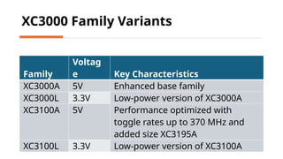
XC3000 Family Variants
Family
Voltag
eKey Characteristics
XC3000A 5V Enhanced base family
XC3000L 3.3V Low-power version of XC3000A
XC3100A 5V Performance optimized with
toggle rates up to 370 MHz and
added size XC3195A
XC3100L 3.3V Low-power version of XC3100A
32.
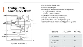
Configurable
Logic Block (CLB)
•Enhancementsover XC2000:
•Functional Highlights:
•Two 4-input LUTs can be combined to implement:
• Any 5-input logic function
• Some 7-input functions
•Slight delay penalty for wider functions.
•Includes two flip-flops for pipelining.
•Internal feedback paths for flip-flop outputs.
•Optimized for state machines and pipelined systems.
Feature XC2000 XC3000
LUT Inputs 3 4
Config Bits
per LUT
8 16
33.
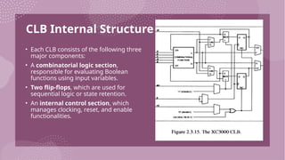
CLB Internal Structure
•Each CLB consists of the following three
major components:
• A combinatorial logic section,
responsible for evaluating Boolean
functions using input variables.
• Two flip-flops, which are used for
sequential logic or state retention.
• An internal control section, which
manages clocking, reset, and enable
functionalities.
34.
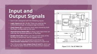
Input and
Output Signals
•Each CLB is designed with the following inputs:
• Logic Inputs (A, B, C, D, E): These are used by the
combinational logic to compute logic functions.
• Clock Input (K): A common clock input shared by both
flip-flops, configurable by the user.
• Asynchronous Reset (RD): A direct reset input that can
override the clocked operation of flip-flops.
• Enable Clock (EC): When Low, the current state of the
flip-flops is preserved, and no update occurs.
• All these inputs are connected to and driven by
interconnect resources located adjacent to each CLB.
• The CLB provides two output lines (X and Y), which can
be routed to other blocks via the interconnect network.
35.
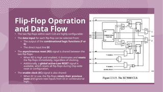
Flip-Flop Operation
and DataFlow
• The two flip-flops within each CLB are highly configurable:
• The data input for each flip-flop can be selected from:
• The output of the combinational logic functions (F or
G)
• The direct input line DI
• The asynchronous reset (RD) signal is shared between the
two flip-flops:
• When RD is High and enabled, it dominates and resets
the flip-flops immediately, regardless of clocking.
• Additionally, a global active-Low RESET signal is
available, which resets all flip-flops during chip-wide
reset or configuration.
• The enable clock (EC) signal is also shared:
• When EC is Low, the flip-flops retain their previous
state and ignore new inputs from DI or combinatorial
logic.
36.
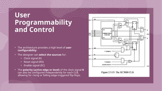
User
Programmability
and Control
• Thearchitecture provides a high level of user
configurability:
• The designer can select the sources for:
• Clock signal (K)
• Reset signal (RD)
• Enable signal (EC)
• The polarity (active edge or level) of the clock signal K
can also be configured independently for each CLB,
allowing for rising or falling edge-triggered flip-flops.
38.
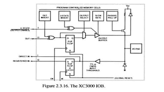
XC3000 Input/Output
Block (IOB)
Overview
•TheXC3000 Input/Output Block (IOB) serves as the
interface between the internal logic of the FPGA and
the external I/O pads.
•Compared to its predecessor (XC2000 IOB), it
introduces enhanced features for improved
performance, predictability, and flexibility in digital
circuit design.
39.
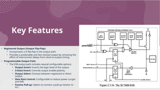
Key Features
• RegisteredOutput (Output Flip-Flop):
• Incorporates a D flip-flop in the output path.
• Provides a predictable and fast clocked output by removing the
effect of interconnect delays from clock-to-output timing.
• Programmable Output Path:
• The IOB output path includes several configurable options:
• Output Invert: Inverts the logic level of the output.
• 3-State Invert: Controls output enable polarity.
• Output Select: Chooses between registered or direct
output.
• Slew Rate Control: Configurable to reduce power surges
and EMI.
• Passive Pull-up: Option to connect a pull-up resistor to
Vcc.
40.
Key Features
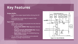
Output Buffer:
•Buffers the output signal before driving the I/O
pad.
• Controlled by 3-state logic to support high-
impedance (Z) state.
Input Path:
• Allows input signal to be passed into the internal
FPGA logic through:
• Direct Path (DIRECT IN): Bypasses internal
flip-flop.
• Registered Path (REGISTERED IN): Passes
through a D flip-flop or latch.
• Both Paths: Enables de-multiplexing (e.g.,
address/data buses).
• TTL or CMOS input threshold can be selected
based on voltage requirements.
41.
Key Features
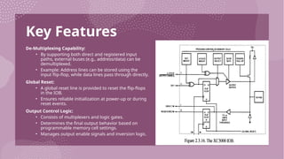
De-Multiplexing Capability:
•By supporting both direct and registered input
paths, external buses (e.g., address/data) can be
demultiplexed.
• Example: Address lines can be stored using the
input flip-flop, while data lines pass through directly.
Global Reset:
• A global reset line is provided to reset the flip-flops
in the IOB.
• Ensures reliable initialization at power-up or during
reset events.
Output Control Logic:
• Consists of multiplexers and logic gates.
• Determines the final output behavior based on
programmable memory cell settings.
• Manages output enable signals and inversion logic.
42.
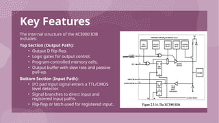
Key Features
The internalstructure of the XC3000 IOB
includes:
Top Section (Output Path):
• Output D flip-flop.
• Logic gates for output control.
• Program-controlled memory cells.
• Output buffer with slew rate and passive
pull-up.
Bottom Section (Input Path):
• I/O pad input signal enters a TTL/CMOS
level detector.
• Signal branches to direct input and
registered input paths.
• Flip-flop or latch used for registered input.
43.
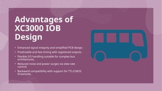
Advantages of
XC3000 IOB
Design
•Enhanced signal integrity and simplified PCB design.
• Predictable and fast timing with registered outputs.
• Flexible I/O handling suitable for complex bus
architectures.
• Reduced noise and power surges via slew rate
control.
• Backward compatibility with support for TTL/CMOS
thresholds.
44.
XC3000 Interconnect Architecture
•Interconnect Structure Overview
• XC3000 features a grid of general
interconnect metal segments.
• Each intersection point includes a
switching matrix allowing
connectivity across horizontal and
vertical tracks.
• Direct connections between
adjacent Configurable Logic Blocks
(CLBs) are available.
45.
Wiring Resources
• Fivegeneral interconnect lines per
direction (horizontal and vertical).
• Three vertical long lines and two
horizontal long lines span the chip.
• Long lines provide low-skew, high-
speed communication and are
essential for global signal
distribution.
46.
Buffers and Bus
Support
•Three-state buffers are distributed along
horizontal long lines (one per CLB).
• These allow construction of on-chip buses
for datapaths.
• Optional pull-up resistors can create
open-drain behavior.
• XC3000 vs XC2000 Buffering:
• XC3000 enables interconnect control
via logic, enhancing flexibility.
• Intelligent buffering and redrive buffers
improve delay handling.
47.
Routing Flexibility
• Enhancedswitching matrix allows rerouting around
congested areas.
• Support for timing-sensitive routing using
selective buffering.
• Redrive buffers are scattered and programmable for
directional driving.
•Block-to-Interconnect Connectivity
• Input PIPs (Programmable Interconnect Points):
Connect CLB inputs to segments in two wiring
channels.
• Control inputs and logic inputs are driven by
specific routing segments.
• Output PIPs: Each CLB output (X and Y) can be
connected to two different wiring channels.
• This increases connectivity and allows signals to
bypass a switchbox
48.
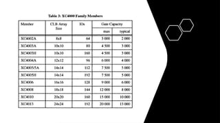
Family Members
and Gate
Capacity
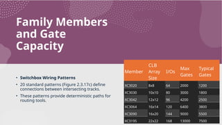
•Switchbox Wiring Patterns
• 20 standard patterns (Figure 2.3.17c) define
connections between intersecting tracks.
• These patterns provide deterministic paths for
routing tools.
Member
CLB
Array
Size
I/Os
Max
Gates
Typical
Gates
XC3020 8x8 64 2000 1200
XC3030 10x10 80 3000 1800
XC3042 12x12 96 4200 2500
XC3064 16x14 120 6400 3800
XC3090 16x20 144 9000 5500
XC3195 22x22 168 13000 7500
49.
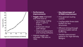
• Performance
Improvements
• Togglerates improved
over time due to:
• Technology scaling
(from 1.2μm to
0.8μm).
• Enhanced critical
path design.
• Advanced placement
and routing software.
• Highest toggle rate
recorded ~240 MHz in
1993.
• Key Advantages of
XC3000 Interconnect
• Fine-grained routing
control.
• Configurable three-state
buffers for bus
structures.
• Efficient timing through
programmable redrive
buffering.
• Flexible interconnect
patterns for high-density
designs.
50.
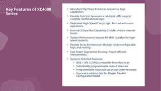
Key Features ofXC4000
Series
• Abundant Flip-Flops: Enhances sequential logic
capabilities.
• Flexible Function Generators: Multiple LUTs support
complex combinational logic.
• Dedicated High-Speed Carry Logic: For fast arithmetic
operations.
• Internal 3-State Bus Capability: Enables shared internal
buses.
• System Performance beyond 80 MHz: Suitable for high-
speed systems.
• Flexible Array Architecture: Modular and reconfigurable
logic and routing.
• Low Power Segmented Routing: Power-efficient
interconnects.
• Systems-Oriented Features:
• IEEE 1149.1 (JTAG) compatible boundary scan
• Individually programmable output slew rate
• Programmable input pull-up or pull-down resistors
• Four extra address bits for Master Parallel
Configuration Mode
51.
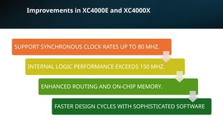
Improvements in XC4000Eand XC4000X
SUPPORT SYNCHRONOUS CLOCK RATES UP TO 80 MHZ.
INTERNAL LOGIC PERFORMANCE EXCEEDS 150 MHZ.
ENHANCED ROUTING AND ON-CHIP MEMORY.
FASTER DESIGN CYCLES WITH SOPHISTICATED SOFTWARE
52.
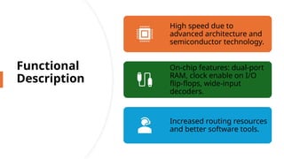
Functional
Description
High speed dueto
advanced architecture and
semiconductor technology.
On-chip features: dual-port
RAM, clock enable on I/O
flip-flops, wide-input
decoders.
Increased routing resources
and better software tools.
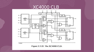
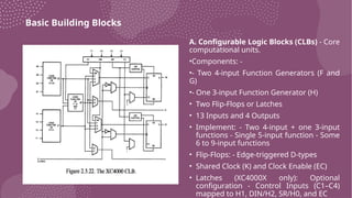
Basic Building Blocks
A.Configurable Logic Blocks (CLBs) - Core
computational units.
•Components: -
•- Two 4-input Function Generators (F and
G)
•- One 3-input Function Generator (H)
• Two Flip-Flops or Latches
• 13 Inputs and 4 Outputs
• Implement: - Two 4-input + one 3-input
functions - Single 5-input function - Some
6 to 9-input functions
• Flip-Flops: - Edge-triggered D-types
• Shared Clock (K) and Clock Enable (EC)
• Latches (XC4000X only): Optional
configuration - Control Inputs (C1–C4)
mapped to H1, DIN/H2, SR/H0, and EC
55.
Basic Building Blocks
•B.Function Generators (F, G, H)
• F and G: Any 4-input Boolean logic
(via LUTs)
• H: 3-input function combining F’,
G’ or external inputs - Outputs:
Routed via X and Y lines
•C. Flip-Flops and Latches
•CLB outputs can be registered or
direct - DIN can drive flip-flop input
directly - Global Set/Reset (GSR)
controls power-up/reset behavior
56.
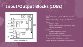
Input/Output Blocks (IOBs)
•Interface between internal logic and external
pins
• Configurable as Input, Output, or Bidirectional
• Inputs:
• Paths I1 and I2
• Optional input register (Flip-Flop or Latch)
• Optional input delay
• Outputs:
• Direct or registered output
• Optional signal inversion
• Separate clocks for input/output registers
• Programmable pull-up/down resistors
• Global Set/Reset (GSR) applies to IOB registers
57.
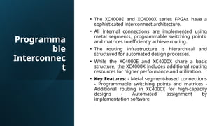
Programma
ble
Interconnec
t
• The XC4000Eand XC4000X series FPGAs have a
sophisticated interconnect architecture.
• All internal connections are implemented using
metal segments, programmable switching points,
and matrices to efficiently achieve routing.
• The routing infrastructure is hierarchical and
structured for automated design processes.
• While the XC4000E and XC4000X share a basic
structure, the XC4000X includes additional routing
resources for higher performance and utilization.
• Key Features: - Metal segment-based connections
- Programmable switching points and matrices -
Additional routing in XC4000X for high-capacity
designs - Automated assignment by
implementation software
58.
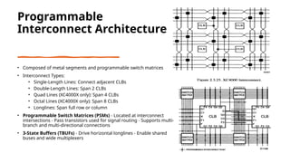
Programmable
Interconnect Architecture
• Composedof metal segments and programmable switch matrices
• Interconnect Types:
• Single-Length Lines: Connect adjacent CLBs
• Double-Length Lines: Span 2 CLBs
• Quad Lines (XC4000X only): Span 4 CLBs
• Octal Lines (XC4000X only): Span 8 CLBs
• Longlines: Span full row or column
• Programmable Switch Matrices (PSMs) - Located at interconnect
intersections - Pass transistors used for signal routing - Supports multi-
branch and multi-directional connections
• 3-State Buffers (TBUFs) - Drive horizontal longlines - Enable shared
buses and wide multiplexers
59.
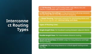
Interconne
ct Routing
Types
a. CLBRouting: Each CLB (Configurable Logic Block) row and
column is associated with routing resources.
b. IOB Routing (VersaRing): A ring around the CLB array connects
I/O with logic blocks and improves pin swapping.
c. Global Routing: Dedicated networks for distributing clocks and
high-fanout signals with minimal delay and skew.
Types of Routing Lines:
Single-length lines: For localized routing between adjacent blocks
Double-length lines: For intermediate distance routing
Quad and Octal lines (XC4000X only): For long-distance and high-
fanout routing
Longlines: For very long distance or critical signal routing across
the chip
60.
CLB Routing Connections
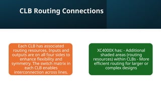
EachCLB has associated
routing resources. Inputs and
outputs are on all four sides to
enhance flexibility and
symmetry. The switch matrix in
each CLB enables
interconnection across lines.
XC4000X has: - Additional
shaded areas (routing
resources) within CLBs - More
efficient routing for larger or
complex designs
61.
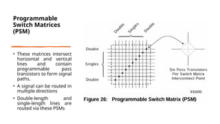
Programmable
Switch Matrices
(PSM)
• Thesematrices intersect
horizontal and vertical
lines and contain
programmable pass
transistors to form signal
paths.
• A signal can be routed in
multiple directions
• Double-length and
single-length lines are
routed via these PSMs
62.
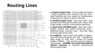
Routing Lines
• a.Single-Length Lines - Connect adjacent blocks
- Eight horizontal and vertical lines per CLB -
High flexibility but less suited for long-distance
routing due to delays at switch matrices.
• b. Double-Length Lines - Span two CLBs - Four
vertical and horizontal lines per CLB - Faster than
single-length, used for intermediate distances
• c. Quad Lines (XC4000X only) - Span four CLBs -
Twelve vertical and twelve horizontal lines -
Buffered switch matrices used - Very fast, ideal
for long, high-fanout nets
• d. Longlines - Span entire chip width or height -
Two horizontal longlines per CLB - Suitable for
wide buses or long nets - Driven by 3-state
buffers (TBUFs) - Can include pull-up resistors
and keepers - XC4000X has enhanced buffered
splitter switches to maintain performance
across large arrays
64.
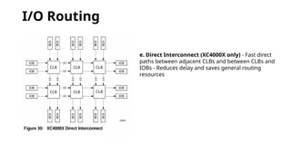
I/O Routing
e. DirectInterconnect (XC4000X only) - Fast direct
paths between adjacent CLBs and between CLBs and
IOBs - Reduces delay and saves general routing
resources
65.
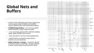
Global Nets and
Buffers
•Used for clock distribution and other high-fanout
control signals. Both XC4000E and XC4000X
support global buffers with dedicated longlines.
• XC4000E Global Buffers: - Four primary global
buffers (BUFGP): Lowest delay and skew
• - Four secondary global buffers (BUFGS): Slightly
higher delay, flexible input sources
• - Each CLB column has four vertical global lines
• - Global buffers accessed through specific
locations via LOC attributes
• Buffer Selection in Design: - Use BUFG, BUFGP,
or BUFGS in HDL or schematic - Design software
chooses buffer based on performance needs
66.
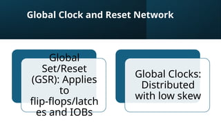
Global Clock andReset Network
Global
Set/Reset
(GSR): Applies
to
flip-flops/latch
es and IOBs
Global Clocks:
Distributed
with low skew
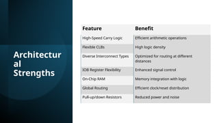
Architectur
al
Strengths
Feature Benefit
High-Speed CarryLogic Efficient arithmetic operations
Flexible CLBs High logic density
Diverse Interconnect Types Optimized for routing at different
distances
IOB Register Flexibility Enhanced signal control
On-Chip RAM Memory integration with logic
Global Routing Efficient clock/reset distribution
Pull-up/down Resistors Reduced power and noise