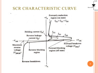
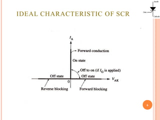
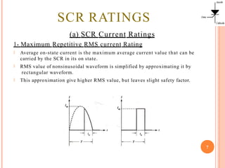
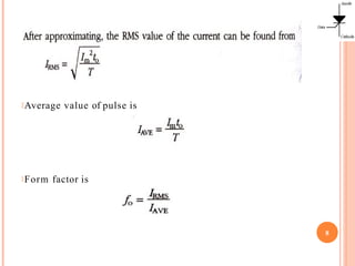
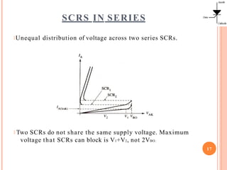
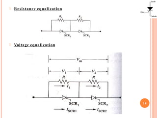
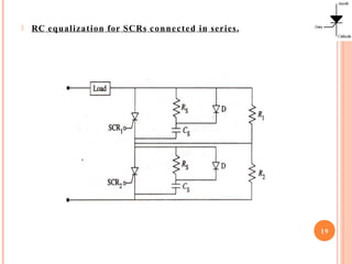
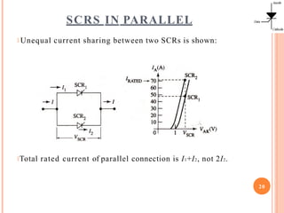
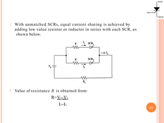
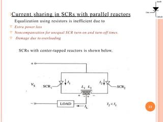
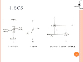
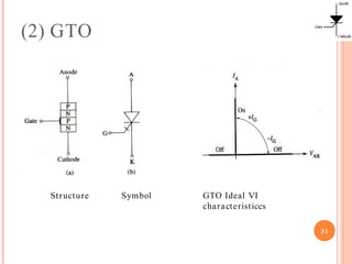
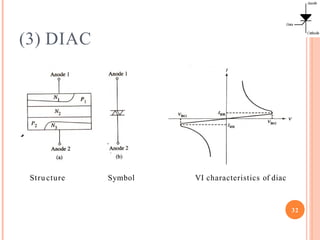
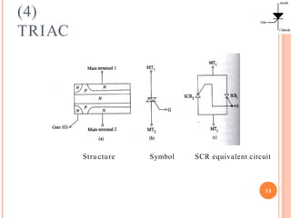
Silicon Controlled Rectifiers
(SCR)
EEN-324
Power Electronics
Thyristor
Devices
1
Power Semiconductor Switches
Power Transistors
Power Diodes
Thyristors
2 layer device
Device
3 layer Device 4 layer
 Thyristor devices can convert and control large amounts of power in
AC or DC systems while using very low power for control.
Thyristor family includes
1 Silicon controlled switch (SCR)
2 Gate-turnoff thyristor (GTO)
3- Triac
4 Diac
5 Silicon controlled switch (SCS)
6- Mos-controlled switch (MCT)

2
INTRODUCTION
SCR is most popular of thyristor family due to its
Fast switching action , small size and high voltage and current
ratings.
It is commonly used in power electronic applications.
 SCR has 3 terminals (gate provides
control)
 al
SCR is turned on by applying +ve gate
sign when anode is +ve with repect to
cathode.
 SCR is turned off by interrupting anode
current.
PNPN structure
3
Symbol
TWO TRANSISTOR MODEL OF SCR
 Gate requires small positive pulse for short duration to turn SCR on.
Once the device is on, the gate signal serves no useful purpose and
can be removed.
4
SCR CHARACTERISTIC CURVE
5
IDEAL CHARACTERISTIC OF SCR
6
SCR RATINGS
(a) SCR Current Ratings
1- Maximum Repetitive RMS current Rating
 Average on-state current is the maximum average current value that can be
carried by the SCR in its on state.
RMS value of nonsinusoidal waveform is simplified by approximating it by
rectangular waveform.
This approximation give higher RMS value, but leaves slight safety factor.


7
Average value of pulse is
Form factor is
8
Knowing the form factor for given waveform, RMS current
can be obtained from
IRMS=fo(IAVE)
Maximum repetitive RMS current is given by
IT(RMS)=fo(IT(AVE))
Conduction angle verses form factor
9
Conduction angle Form factor (fo)
(θ)
20° 5.0
40° 3.5
60° 2.7
80° 2.3
100° 2.0
120° 1.8
140° 1.6
160° 1.4
CONDUCTION ANGLE
Duration for which SCR is on. It is measured as
shown
10
2- Surge Current Rating
Peak anode current that SCR can handle for brief duration.
11
3 Latching current
Minimum anode current that must flow through the SCR in order
for it to stay on initially after gate signal is removed.
4 Holding Current
Minimum value of anode current, required to maintain SCR in
conducting state.
(B) SCR VOLTAGE RATINGS
12
1 Peak repetitive forward blocking voltage
Maximum instantaneous voltage that SCR can block in forward
direction.
2 Peak Repetitive Reverse Voltage
Maximum instantaneous voltage that SCR can
withstand, without breakdown, in reverse direction.
3 Non-repetitive peak reverse voltage
Maximum transient reverse voltage that SCR can
withstand.
(C) SCR RATE-OF-CHANGE RATINGS
1 (di/dt rating)
Critical rate of rise of on-state current. It is the rate at which anode current
increases and must be less than rate at which conduction area increases.
To prevent damage to SCR by high di/dt value, small inductance is added in series
with device. Vaue of required inductance is
L>= Vp
(di/dt)max
2 dv/dt rating
Maximum rise time of a voltage pulse that can be applied to the SCR in the off state
without causing it to fire. Unscheduled firing due to high value of dv/dt can be
prevented by using RC snubber circuit.
13
(D) GATE PARAMETERS
1 Maximum Gate Peak Inverse Voltage
Maximum value of negative DC voltage that can be applied without damaging the gate-
cathode junction.
2 Maximum Gate Trigger Current
Maximum DC gate current allowed to turn on the device.
3 Maximum gate trigger voltage
DC voltage necessary to produce maximum gate trigger current.
4 Maximum Gate Power Dissipation
Maximum instantaneous product of gate current and gate voltage that can exist during
forward-bias.
5 Minimum gate trigger voltage
Minimum DC gate-to-cathode voltage required to trigger the SCR.
6-Minimum gate trigger current
Minimum DC gate current necessary to turn SCR on.
14
Series and Parallel
SCR Connections
15
SCRs are connected in series and parallel to
extend voltage and current ratings.
16
For high-voltage, high-current applications, series-
parallel combinations of SCRs are used.
SCRS IN SERIES
Unequal distribution of voltage across two series SCRs.
 Two SCRs do not share the same supply voltage. Maximum
voltage that SCRs can block is V1+V2, not 2VBO.
17
 Resistance equalization
 Voltage equalization
18
 RC equalization for SCRs connected in series.
19
SCRS IN PARALLEL
 Unequal current sharing between two SCRs is shown:
Total rated current of parallel connection is I1+I2, not 2I2.
20
 With unmatched SCRs, equal current sharing is achieved by
adding low value resistor or inductor in series with each SCR, as
shown below.
 Value of resistance R is obtained from:
R=V1-V2
I2-I1
21
Current sharing in SCRs with parallel reactors
Equalization using resistors is inefficient due to



Extra power loss
Noncompansation for unequal SCR turn-on and turn-off times.
Damage due to overloading
SCRs with center-tapped reactors is shown below.
22
SCR Gate-Triggering
Circuits
23
Triggering circuits provide firing signal to turn
on the SCR at precisely the correct time.
24
Firing circuits must have following properties
1. Produce gate signal of suitable magnitude and sufficiently
short rise time.
2. Produce gate signal of adequate duration.
3. Provide accurate firing control over the required range.
4. Ensure that triggering does not occur from false signals or
noise
5. In AC applications, ensure that the gate signal is applied
when the SCR is forward-biased
6. In three-phase circuits, provide gate pulses that are 120°
apart
with respect to the reference point
7. Ensure simultaneous triggering of SCRs connected in series
or in parallel.
SCR Turnoff (Commutation)
Circuits
25
What is Commutation?
The process of turning off an SCR is
called commutation.
26
It is achieved by
1. Reducing anode current below holding current
2. Make anode negative with respect to cathode
Types of commutation are:
3. Natural or line commutation
4. Forced commutation
SCR TURNOFF METHODS
1. Diverting the anode current to an alternate path
2. Shorting the SCR from anode to cathode
3. Applying a reverse voltage (by making the
cathode positive with respect to the anode) across
the SCR
4. Forcing the anode current to zero for a brief period
5. Opening the external path from its anode supply
voltage
6. Momentarily reducing supply voltage to
zero
38
Other members of
Thyristor Family
28
OTHER TYPES OF
29
THYRISTORS
1. Silicon Controlled Switch (SCS)
2. Gate Turnoff Thyristor (GTO)
3. DIAC
4. TRIAC
5. MOS-Controlled Thyristor (MCT)
1. SCS
Structure Symbol Equivalent circuit for SCS
30
(2) GTO
Structure Symbol GTO Ideal VI
characteristiccs
31
(3) DIAC
Stru cture Symbol VI characteristics of diac
32
(4)
TRIAC
Stru cture
33
Symbol SCR equivalent circuit
TRIAC VI CHARACTERISTICS
34

SCR Silicon controlled rectifierSilicon controlled rectifier

  • 1.
  • 2.
    Power Semiconductor Switches PowerTransistors Power Diodes Thyristors 2 layer device Device 3 layer Device 4 layer  Thyristor devices can convert and control large amounts of power in AC or DC systems while using very low power for control. Thyristor family includes 1 Silicon controlled switch (SCR) 2 Gate-turnoff thyristor (GTO) 3- Triac 4 Diac 5 Silicon controlled switch (SCS) 6- Mos-controlled switch (MCT)  2
  • 3.
    INTRODUCTION SCR is mostpopular of thyristor family due to its Fast switching action , small size and high voltage and current ratings. It is commonly used in power electronic applications.  SCR has 3 terminals (gate provides control)  al SCR is turned on by applying +ve gate sign when anode is +ve with repect to cathode.  SCR is turned off by interrupting anode current. PNPN structure 3 Symbol
  • 4.
    TWO TRANSISTOR MODELOF SCR  Gate requires small positive pulse for short duration to turn SCR on. Once the device is on, the gate signal serves no useful purpose and can be removed. 4
  • 5.
  • 6.
  • 7.
    SCR RATINGS (a) SCRCurrent Ratings 1- Maximum Repetitive RMS current Rating  Average on-state current is the maximum average current value that can be carried by the SCR in its on state. RMS value of nonsinusoidal waveform is simplified by approximating it by rectangular waveform. This approximation give higher RMS value, but leaves slight safety factor.   7
  • 8.
    Average value ofpulse is Form factor is 8
  • 9.
    Knowing the formfactor for given waveform, RMS current can be obtained from IRMS=fo(IAVE) Maximum repetitive RMS current is given by IT(RMS)=fo(IT(AVE)) Conduction angle verses form factor 9 Conduction angle Form factor (fo) (θ) 20° 5.0 40° 3.5 60° 2.7 80° 2.3 100° 2.0 120° 1.8 140° 1.6 160° 1.4
  • 10.
    CONDUCTION ANGLE Duration forwhich SCR is on. It is measured as shown 10
  • 11.
    2- Surge CurrentRating Peak anode current that SCR can handle for brief duration. 11 3 Latching current Minimum anode current that must flow through the SCR in order for it to stay on initially after gate signal is removed. 4 Holding Current Minimum value of anode current, required to maintain SCR in conducting state.
  • 12.
    (B) SCR VOLTAGERATINGS 12 1 Peak repetitive forward blocking voltage Maximum instantaneous voltage that SCR can block in forward direction. 2 Peak Repetitive Reverse Voltage Maximum instantaneous voltage that SCR can withstand, without breakdown, in reverse direction. 3 Non-repetitive peak reverse voltage Maximum transient reverse voltage that SCR can withstand.
  • 13.
    (C) SCR RATE-OF-CHANGERATINGS 1 (di/dt rating) Critical rate of rise of on-state current. It is the rate at which anode current increases and must be less than rate at which conduction area increases. To prevent damage to SCR by high di/dt value, small inductance is added in series with device. Vaue of required inductance is L>= Vp (di/dt)max 2 dv/dt rating Maximum rise time of a voltage pulse that can be applied to the SCR in the off state without causing it to fire. Unscheduled firing due to high value of dv/dt can be prevented by using RC snubber circuit. 13
  • 14.
    (D) GATE PARAMETERS 1Maximum Gate Peak Inverse Voltage Maximum value of negative DC voltage that can be applied without damaging the gate- cathode junction. 2 Maximum Gate Trigger Current Maximum DC gate current allowed to turn on the device. 3 Maximum gate trigger voltage DC voltage necessary to produce maximum gate trigger current. 4 Maximum Gate Power Dissipation Maximum instantaneous product of gate current and gate voltage that can exist during forward-bias. 5 Minimum gate trigger voltage Minimum DC gate-to-cathode voltage required to trigger the SCR. 6-Minimum gate trigger current Minimum DC gate current necessary to turn SCR on. 14
  • 15.
  • 16.
    SCRs are connectedin series and parallel to extend voltage and current ratings. 16 For high-voltage, high-current applications, series- parallel combinations of SCRs are used.
  • 17.
    SCRS IN SERIES Unequaldistribution of voltage across two series SCRs.  Two SCRs do not share the same supply voltage. Maximum voltage that SCRs can block is V1+V2, not 2VBO. 17
  • 18.
     Resistance equalization Voltage equalization 18
  • 19.
     RC equalizationfor SCRs connected in series. 19
  • 20.
    SCRS IN PARALLEL Unequal current sharing between two SCRs is shown: Total rated current of parallel connection is I1+I2, not 2I2. 20
  • 21.
     With unmatchedSCRs, equal current sharing is achieved by adding low value resistor or inductor in series with each SCR, as shown below.  Value of resistance R is obtained from: R=V1-V2 I2-I1 21
  • 22.
    Current sharing inSCRs with parallel reactors Equalization using resistors is inefficient due to    Extra power loss Noncompansation for unequal SCR turn-on and turn-off times. Damage due to overloading SCRs with center-tapped reactors is shown below. 22
  • 23.
  • 24.
    Triggering circuits providefiring signal to turn on the SCR at precisely the correct time. 24 Firing circuits must have following properties 1. Produce gate signal of suitable magnitude and sufficiently short rise time. 2. Produce gate signal of adequate duration. 3. Provide accurate firing control over the required range. 4. Ensure that triggering does not occur from false signals or noise 5. In AC applications, ensure that the gate signal is applied when the SCR is forward-biased 6. In three-phase circuits, provide gate pulses that are 120° apart with respect to the reference point 7. Ensure simultaneous triggering of SCRs connected in series or in parallel.
  • 25.
  • 26.
    What is Commutation? Theprocess of turning off an SCR is called commutation. 26 It is achieved by 1. Reducing anode current below holding current 2. Make anode negative with respect to cathode Types of commutation are: 3. Natural or line commutation 4. Forced commutation
  • 27.
    SCR TURNOFF METHODS 1.Diverting the anode current to an alternate path 2. Shorting the SCR from anode to cathode 3. Applying a reverse voltage (by making the cathode positive with respect to the anode) across the SCR 4. Forcing the anode current to zero for a brief period 5. Opening the external path from its anode supply voltage 6. Momentarily reducing supply voltage to zero 38
  • 28.
  • 29.
    OTHER TYPES OF 29 THYRISTORS 1.Silicon Controlled Switch (SCS) 2. Gate Turnoff Thyristor (GTO) 3. DIAC 4. TRIAC 5. MOS-Controlled Thyristor (MCT)
  • 30.
    1. SCS Structure SymbolEquivalent circuit for SCS 30
  • 31.
    (2) GTO Structure SymbolGTO Ideal VI characteristiccs 31
  • 32.
    (3) DIAC Stru ctureSymbol VI characteristics of diac 32
  • 33.
  • 34.