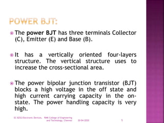
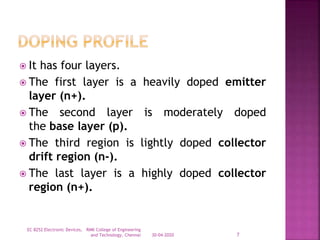
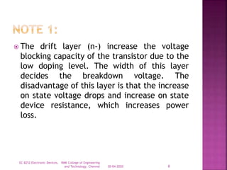
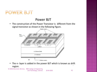
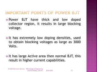
By
Shaik Hedayath Basha
Assistant Professor
RMK College of Engineering and Technology
30-04-2020EC 8252 Electronic Devices, RMK College of Engineering and Technology, Chennai 1
 BJT is Bipolar Junction Transistor, it has three
terminals: Emitter, Base and Collector.
 The Base area smaller and is lightly doped
than Collector and Emitter.
 The Collector area less than or equal to
Emitter area.
 The Emitter area is highly doped compared
to Base and Collector
30-04-2020
EC 8252 Electronic Devices, RMK College of Engineering
and Technology, Chennai 2
30-04-2020
EC 8252 Electronic Devices, RMK College of Engineering
and Technology, Chennai 3
30-04-2020
EC 8252 Electronic Devices, RMK College of Engineering
and Technology, Chennai 4
 The power BJT has three terminals Collector
(C), Emitter (E) and Base (B).
 It has a vertically oriented four-layers
structure. The vertical structure uses to
increase the cross-sectional area.
 The power bipolar junction transistor (BJT)
blocks a high voltage in the off state and
high current carrying capacity in the on-
state. The power handling capacity is very
high.
30-04-2020
EC 8252 Electronic Devices, RMK College of Engineering
and Technology, Chennai 5
30-04-2020
EC 8252 Electronic Devices, RMK College of Engineering
and Technology, Chennai 6
 It has four layers.
 The first layer is a heavily doped emitter
layer (n+).
 The second layer is moderately doped
the base layer (p).
 The third region is lightly doped collector
drift region (n-).
 The last layer is a highly doped collector
region (n+).
30-04-2020
EC 8252 Electronic Devices, RMK College of Engineering
and Technology, Chennai 7
 The drift layer (n-) increase the voltage
blocking capacity of the transistor due to the
low doping level. The width of this layer
decides the breakdown voltage. The
disadvantage of this layer is that the increase
on state voltage drops and increase on state
device resistance, which increases power
loss.
30-04-2020
EC 8252 Electronic Devices, RMK College of Engineering
and Technology, Chennai 8
 The power handling capacity of the power
transistor is very large. So, they have to
dissipate power in the form of heat.
Sometimes, heatsink uses to increase
effective area and therefore increase power
dissipation capacity. the heatsink made from
metal
30-04-2020
EC 8252 Electronic Devices, RMK College of Engineering
and Technology, Chennai 9
30-04-2020
EC 8252 Electronic Devices, RMK College of Engineering
and Technology, Chennai 10
 It is designed to effectively manage the
power dissipation.
 To avoid Krik effect.
30-04-2020
EC 8252 Electronic Devices, RMK College of Engineering
and Technology, Chennai 11
 Krik Effect: The Krik effect occurs at high
current densities and causes a dramatic
increase in the transit time of a bipolar
transistor. This effect is due to the charge
density associated with the current density
passing through the base collector region.
 As charge density exceed in the depletion
region, the depletion region ceases to exist.
 Krik effect can be eliminated by increasing
the collector doping.
30-04-2020
EC 8252 Electronic Devices, RMK College of Engineering
and Technology, Chennai 12
 Power BJT have thick and low doped
collector region, it results in large blocking
voltage.
 It has extremely low doping densities, used
to obtain blocking voltages as large as 3000
Volts.
 It has large Active area then normal BJT, this
result in higher current capabilities.
30-04-2020
EC 8252 Electronic Devices, RMK College of Engineering
and Technology, Chennai 13
The I-V characteristic of Power BJT divides into
four regions.
 Cut-off region
 Active region
 Quasi-saturation region
 Hard saturation region
30-04-2020
EC 8252 Electronic Devices, RMK College of Engineering
and Technology, Chennai 14
30-04-2020
EC 8252 Electronic Devices, RMK College of Engineering
and Technology, Chennai 15
 The BE and CB both junctions are reverse
bias. The base current IB=0 and collector
current IC is equal to the reverse leakage
current ICEO. The region below the
characteristic for IB=0 is cut-off region. In
this region, BJT offers large resistance to the
flow of current. Hence it is equivalent to an
open circuit.
30-04-2020
EC 8252 Electronic Devices, RMK College of Engineering
and Technology, Chennai 16
 The BE junction is forward bias and CB
junction is reverse bias. The collector
current IC increase slightly with an increase
in the voltage VCE if IB is increased. The
relation of IB and IC is, IC=βdcIB is true in the
active region.
 If BJT uses as an amplifier or as a series pass
transistor in the voltage regulator, it
operates in this region. The dynamic
resistance in this region is large. The power
dissipation is maximum
30-04-2020
EC 8252 Electronic Devices, RMK College of Engineering
and Technology, Chennai 17
 Quasi-saturation region is between the hard
saturation and active region. This region exists
due to the lightly doped drift layer. When the
BJT operates at high frequency, it is operated in
this region. Both junctions are forward bias.
 The device offers low resistance compared to
the active region. So, power loss is less. In this
region, the device does not go into deep
saturation. So, it can turn off quickly. Therefore,
we can use for higher frequency applications
30-04-2020
EC 8252 Electronic Devices, RMK College of Engineering
and Technology, Chennai 18
 The Power BJT push into the hard-saturation
region from the quasi-saturation region by
increasing the base current. This region is
also known as deep saturation region. The
resistance offers in this region is minimum. It
is even less than the quasi-saturation region.
So, when the BJT operates in this region,
power dissipation is minimum.
30-04-2020
EC 8252 Electronic Devices, RMK College of Engineering
and Technology, Chennai 19
 The device acts as a closed switch when it
operates in this region. But it needs more
time to turn off. So, this region is suitable
only for low-frequency switching application.
In this region, both junctions are forward
bias. The collector current is not
proportional to the base current, IC remains
almost constant at IC(sat) and independent
from the value of base current.
30-04-2020
EC 8252 Electronic Devices, RMK College of Engineering
and Technology, Chennai 20
 Switched Mode Power Supply (SMPS)
 Power Amplifier
 Relay and Drivers
 AC motor speed controller
 DC/AC inverter
 As series pass transistor in the regulated
power supply
 The audio amplifier in the stereo system
 Power control circuit
30-04-2020
EC 8252 Electronic Devices, RMK College of Engineering
and Technology, Chennai 21

Power BJT

  • 1.
    By Shaik Hedayath Basha AssistantProfessor RMK College of Engineering and Technology 30-04-2020EC 8252 Electronic Devices, RMK College of Engineering and Technology, Chennai 1
  • 2.
     BJT isBipolar Junction Transistor, it has three terminals: Emitter, Base and Collector.  The Base area smaller and is lightly doped than Collector and Emitter.  The Collector area less than or equal to Emitter area.  The Emitter area is highly doped compared to Base and Collector 30-04-2020 EC 8252 Electronic Devices, RMK College of Engineering and Technology, Chennai 2
  • 3.
    30-04-2020 EC 8252 ElectronicDevices, RMK College of Engineering and Technology, Chennai 3
  • 4.
    30-04-2020 EC 8252 ElectronicDevices, RMK College of Engineering and Technology, Chennai 4
  • 5.
     The powerBJT has three terminals Collector (C), Emitter (E) and Base (B).  It has a vertically oriented four-layers structure. The vertical structure uses to increase the cross-sectional area.  The power bipolar junction transistor (BJT) blocks a high voltage in the off state and high current carrying capacity in the on- state. The power handling capacity is very high. 30-04-2020 EC 8252 Electronic Devices, RMK College of Engineering and Technology, Chennai 5
  • 6.
    30-04-2020 EC 8252 ElectronicDevices, RMK College of Engineering and Technology, Chennai 6
  • 7.
     It hasfour layers.  The first layer is a heavily doped emitter layer (n+).  The second layer is moderately doped the base layer (p).  The third region is lightly doped collector drift region (n-).  The last layer is a highly doped collector region (n+). 30-04-2020 EC 8252 Electronic Devices, RMK College of Engineering and Technology, Chennai 7
  • 8.
     The driftlayer (n-) increase the voltage blocking capacity of the transistor due to the low doping level. The width of this layer decides the breakdown voltage. The disadvantage of this layer is that the increase on state voltage drops and increase on state device resistance, which increases power loss. 30-04-2020 EC 8252 Electronic Devices, RMK College of Engineering and Technology, Chennai 8
  • 9.
     The powerhandling capacity of the power transistor is very large. So, they have to dissipate power in the form of heat. Sometimes, heatsink uses to increase effective area and therefore increase power dissipation capacity. the heatsink made from metal 30-04-2020 EC 8252 Electronic Devices, RMK College of Engineering and Technology, Chennai 9
  • 10.
    30-04-2020 EC 8252 ElectronicDevices, RMK College of Engineering and Technology, Chennai 10
  • 11.
     It isdesigned to effectively manage the power dissipation.  To avoid Krik effect. 30-04-2020 EC 8252 Electronic Devices, RMK College of Engineering and Technology, Chennai 11
  • 12.
     Krik Effect:The Krik effect occurs at high current densities and causes a dramatic increase in the transit time of a bipolar transistor. This effect is due to the charge density associated with the current density passing through the base collector region.  As charge density exceed in the depletion region, the depletion region ceases to exist.  Krik effect can be eliminated by increasing the collector doping. 30-04-2020 EC 8252 Electronic Devices, RMK College of Engineering and Technology, Chennai 12
  • 13.
     Power BJThave thick and low doped collector region, it results in large blocking voltage.  It has extremely low doping densities, used to obtain blocking voltages as large as 3000 Volts.  It has large Active area then normal BJT, this result in higher current capabilities. 30-04-2020 EC 8252 Electronic Devices, RMK College of Engineering and Technology, Chennai 13
  • 14.
    The I-V characteristicof Power BJT divides into four regions.  Cut-off region  Active region  Quasi-saturation region  Hard saturation region 30-04-2020 EC 8252 Electronic Devices, RMK College of Engineering and Technology, Chennai 14
  • 15.
    30-04-2020 EC 8252 ElectronicDevices, RMK College of Engineering and Technology, Chennai 15
  • 16.
     The BEand CB both junctions are reverse bias. The base current IB=0 and collector current IC is equal to the reverse leakage current ICEO. The region below the characteristic for IB=0 is cut-off region. In this region, BJT offers large resistance to the flow of current. Hence it is equivalent to an open circuit. 30-04-2020 EC 8252 Electronic Devices, RMK College of Engineering and Technology, Chennai 16
  • 17.
     The BEjunction is forward bias and CB junction is reverse bias. The collector current IC increase slightly with an increase in the voltage VCE if IB is increased. The relation of IB and IC is, IC=βdcIB is true in the active region.  If BJT uses as an amplifier or as a series pass transistor in the voltage regulator, it operates in this region. The dynamic resistance in this region is large. The power dissipation is maximum 30-04-2020 EC 8252 Electronic Devices, RMK College of Engineering and Technology, Chennai 17
  • 18.
     Quasi-saturation regionis between the hard saturation and active region. This region exists due to the lightly doped drift layer. When the BJT operates at high frequency, it is operated in this region. Both junctions are forward bias.  The device offers low resistance compared to the active region. So, power loss is less. In this region, the device does not go into deep saturation. So, it can turn off quickly. Therefore, we can use for higher frequency applications 30-04-2020 EC 8252 Electronic Devices, RMK College of Engineering and Technology, Chennai 18
  • 19.
     The PowerBJT push into the hard-saturation region from the quasi-saturation region by increasing the base current. This region is also known as deep saturation region. The resistance offers in this region is minimum. It is even less than the quasi-saturation region. So, when the BJT operates in this region, power dissipation is minimum. 30-04-2020 EC 8252 Electronic Devices, RMK College of Engineering and Technology, Chennai 19
  • 20.
     The deviceacts as a closed switch when it operates in this region. But it needs more time to turn off. So, this region is suitable only for low-frequency switching application. In this region, both junctions are forward bias. The collector current is not proportional to the base current, IC remains almost constant at IC(sat) and independent from the value of base current. 30-04-2020 EC 8252 Electronic Devices, RMK College of Engineering and Technology, Chennai 20
  • 21.
     Switched ModePower Supply (SMPS)  Power Amplifier  Relay and Drivers  AC motor speed controller  DC/AC inverter  As series pass transistor in the regulated power supply  The audio amplifier in the stereo system  Power control circuit 30-04-2020 EC 8252 Electronic Devices, RMK College of Engineering and Technology, Chennai 21