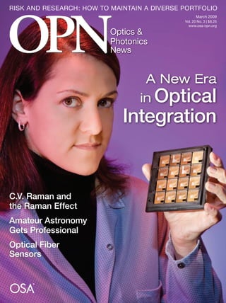
March 2009
Vol. 20 No. 3 | $8.25
www.osa-opn.org
RISK AND RESEARCH: HOW TO MAINTAIN A DIVERSE PORTFOLIO
Optics &
Photonics
News
A New Era
in Optical
Integration
C.V. Raman and
the Raman Effect
Amateur Astronomy
Gets Professional
Optical Fiber
Sensors
OPN March 2009 | 1
FEATURES | CONTENTS
[ COVER STORY ]
20	 A New Era in Optical Integration
The Internet is increasingly taxing optical networks, and conventional network architecture
cannot provide the scalability required to meet this demand. These authors advise
telecommunications professionals to follow the lead of the microelectronics industry—
by focusing on integrated solutions.
Jacco L. Pleumeekers, Peter W. Evans, Wei Chen, Richard P. Schneider Jr. and
Radha Nagarajan
26 	 Optical Fiber High-Temperature Sensors
Optical fiber sensors allow researchers and engineers to make accurate, reliable
measurements under high-temperature conditions.
Anbo Wang, Yizheng Zhu and Gary Pickrell
32	 The Professional World of Amateur Astronomy
The work of today’s amateur astronomers goes far beyond peering through a telescope on
a lonely mountaintop. Thanks to advances in solid-state imaging, software and inexpensive
optics, they are collecting professional-quality data and making their own discoveries.
Patricia Daukantas
40 	 C.V. Raman and the Raman Effect
Barry Masters describes the life and legacy of one of the most important optical
scientists of the 20th
century.
Barry R. Masters
New technologies
will be needed
for photonic
integration to scale
to a “photonic
Moore’s Law.”
COVER PHOTO: Infinera’s
Sheila Hurtt holds a tray
containing 16 photonic
integrated circuits.
Photo by Gene Lee.
OPN March 2009
Vol. 20, No. 3
Infinera’s Leigh Wade configures a
system at the company’s system lab.
The DTN system can accommodate
four photonic-integrated-circuit-
based line cards, each with data
transmission capacity of 100 Gb/s.
Gene Lee/Infinera
2 | OPN March 2009 www.osa-opn.org
CONTENTS | DEPARTMENTS
8 Scatterings
Nanoscopy uncovers cells’ secrets; lasing
mechanism depends on electron momentum;
powerful light source for X-ray microscopy.
Yvonne Carts-Powell
10 Optics Innovations
CREOL’s tech-transfer success stories.
Jenna Reiser and James Pearson
12 Light Touch
The yellow sun paradox.
Stephen R. Wilk
14 Conversations in Optics
OPN talks with Philippe
Morin, president of
Metro Ethernet
Networks at Nortel
and OFC/NFOEC
keynote speaker.
16 Viewpoint
Risk and research:
Maintaining a
diverse portfolio.
Ken Baldwin
18 The History of OSA
George Ellery Hale and the
Yerkes Observatory.
John N. Howard
48 In Memory
Remembering Richard E. Grojean,
a professor emeritus at Northeastern
University; Robert Hilbert, president
and chief executive officer of ORA; and
James L. Fergason, the father of the
liquid crystal industry.
4 President’s Message
7 Letters
46 OSA Today
50 Book Reviews
52 Product Profiles
54 Marketplace
56 After Image
10
OPN Optics & Photonics News (ISSN 1047-6938), Vol. 20, No. 3 © 2009, Optical Society of America. OPN is published monthly except bimonthly July-August by the Optical
Society of America, 2010 Massachusetts Ave., N.W., Washington, D.C. 20036; 202.223.8130; Fax 202.223.1096; Email opn@osa.org; Web www.osa-opn.org. OPN was
published as Optics News from 1975-1989. (CODEN OPPHEL; GST #133618991; IPM #0895431). OSA is a not-for-profit society founded in 1916. Authorization to photocopy
items for internal or personal use, or the internal or personal use of specific clients, is granted by the Optical Society of America, provided that the base fee of $6 per copy is paid
directly to the Copyright Clearance Center, 27 Congress St., Salem, Mass. 01970-5575. For those organizations that have been granted a photocopy license by CCC, a separate system of payment
has been arranged. The fee code for users of the Transactional Report Service is 0098-907X/99 $6. Permission is granted to quote excerpts from articles in this publication in scientific works with the
customary acknowledgment of the name of the publication, page, year and name of the Society. Reproduction of figures and tables is likewise permitted in other articles and books provided that the same
information is printed with them and notification is given to the Optical Society of America. 2009 nonmember and library subscription rates (domestic): $100/year. Membership in the Optical Society of
America includes $7 from membership dues to be applied to a member subscription. Application to mail at Periodicals Postage pending at Washington, DC, and additional mailing offices. POSTMASTER:
Send address changes to OPN Optics & Photonics News, 2010 Massachusetts Ave., N.W., Washington, DC 20036. Subscriptions, missing copies, change of address: Optical Society of America,
Subscription Fulfillment Services, 2010 Massachusetts Ave., N.W., Washington, D.C. 20036; 800.766.4672. Back numbers, single issue, and foreign rates
on request. Printed in the United States. OSA is a registered trademark of the Optical Society of America. ©2009. The content and opinions expressed in
feature articles and departments in Optics & Photonics News and its occasional supplement, OPN Trends, are those of the authors and guest editors and
do not necessarily reflect those of OPN or the Optical Society of America.
 
Jacquephoto.com
Fraunhofer Institute
for Laser Technology ILT
OPN talks with Philippe
The History of OSA Fraunhofer Institute
8
CODE V’s fast wavefront
differential tolerancing
gives you the accuracy
of a long Monte Carlo
analysis—in just seconds.
Not only does CODE V
provide an accurate statistical
analysis of the expected RMS or MTF
performance with selected tolerances
and compensators, it also identifies
the most sensitive, performance-
driving tolerances. Utilizing a new
Singular Value Decomposition
algorithm, CODE V can even identify
the best compensators for your
system from all the possible
compensators.
CODE V’s unique Interactive
Tolerancing leverages the speed of
wavefront differential tolerancing
to allow you to make changes to the
tolerance values and instantly see the
impact on performance. In addition,
CODE V supports slope error and
RMS surface error tolerance types
for specifying tolerances on aspheric
surfaces in a way that can be modeled
in the software and measured by
your fabricator.
Try CODE V on your tolerancing
problem.You’ll love the results.
• Achieve fast system tolerancing
with the accuracy of a Monte
Carlo analysis of thousands of
trials.
• Let CODE V automatically select
the most leveraged subset of
compensators from a larger list
for improved manufacturability
and lowered costs.
• Tolerance aspheric surface
errors that are easily measured
in production using surface
profilometry.
• Instantly see the impact of
tolerance changes on system
performance.
• Create tolerance-insensitive
designs by optimizing for best
fabricated performance.
Corporate Headquarters: 3280 East Foothill Boulevard, Pasadena, CA 91107-3103 (626) 795-9101
Fax (626) 795-0184 E-mail: info@opticalres.com Web: www.opticalres.com
Offices: Tucson, AZ | Westborough, MA
©2008 Optical Research Associates. CODE V is a registered trademark of Optical Research Associates.
Fewer Trials…No ErrorsDesign manufacturable, high-performance optics with CODE V’s
comprehensive tolerancing features.
OPTICAL DESIGN SOFTWARE
www.opticalres.com
CODEV_OPN.indd 1 3/25/08 12:27:28 PM
4 | OPN March 2009 www.osa-opn.org
PRESIDENT’S MESSAGE
t several crisis points over the last century, large teams of high-level scientists and
engineers mobilized to spearhead intense efforts to solve critical societal problems. These
efforts not only produced the desired scientific breakthroughs, but also led to significant
investments in basic and applied research and renewed public awareness of the scientific
community’s tremendous capacity for innovation. The current energy crisis calls for just
such a massive, coordinated effort. We are at a unique moment in time, with a new admin-
istration in the United States committed to supporting initiatives focused on overcoming
the energy and environmental crises.
Recently, President Barack Obama, in his speech nominating OSA member Steven Chu
as the new U.S. Secretary of Energy, announced that the pursuit of alternative and renew-
able energy sources would be a “guiding purpose of the Department of Energy as well as a
national mission.” Noting that energy independence lies “in the power of wind and solar
[and]...in the innovation of our scientists and entrepreneurs,” Obama called for a “sus-
tained, all-hands-on-deck effort” to address global energy concerns.
Renewable energy based on solar, wind and biomass offers viable alternatives to fossil
fuels. These options can greatly diminish a nation’s dependence on foreign energy, reduce
greenhouse gas emissions, protect and preserve natural resources and stimulate economic
growth through the development of new industries and technologies.
The OSA community is uniquely positioned to play a prominent role in the further devel-
opment of solar and other renewable energy technologies. We have the knowledge, expertise
and resources to achieve significant advances in both research and applications—but we can
only be successful if we marshal our resources and make the commitment to join in the “all-
hands-on-deck effort” that President Obama and Secretary Chu are organizing.
In June 2008, OSA held a very successful two-day Solar Energy topical meeting at
Stanford University. At this meeting, an international group of leading scientists reported
on new photovoltaic materials in combination with nanostructured electrodes, flat panel
photovoltaic devices incorporating plasmonic resonances and nonimaging concentrators, all
of which have the potential to significantly enhance solar energy efficiency. We are currently
planning a second solar meeting to be held at MIT from June 24-25, 2009. I encourage all
OSA members interested in this area to attend.
In addition, we are forming an officers’ advisory group chaired by OSA President-elect
Jim Wyant to lead our activities as OSA expands its efforts in solar energy. I invite all OSA
members as well as the greater optics and photonics community to volunteer to put your
expertise to work on this vital challenge.
If you’d like join me in this effort, please send a message to osapresident@osa.org. Work-
ing together, we can be a significant force in solving the world’s energy needs.
— Thomas M. Baer
OSA President
We are forming
an officers’
advisory group
chaired by OSA
President-elect
Jim Wyant to lead
our activities as
OSA expands its
efforts in solar
energy. I invite all
OSA members to
put your expertise
to work on this
vital challenge.”
A
“
OPN March 2009 | 5
OEM
Biomedical
R&DImaging
Laser
Applications
NEED STOCK
OR CUSTOM
FILTERS?
need a volume or
custom quote?
ContaCt our
sales department today
or to receive your FREE catalog!
more optics
more technology
more service
•	 More	than	1,300	Stock	Filters		
	 Available	for	Same	Day	Shipping
•	 Custom	Designs	&	Coatings	Available	-		
	 Over	25	Years	Coating	Experience
•	 High	Transmission,	Deep	Blocking
Fast Delivery
Free Technical Support
800.363.1992 | www.edmundoptics.com/OP
Visit us at
Defense,security,& sensing
Booth 1029
MANAGING EDITOR Christina E. Folz
CREATIVE DIRECTOR Alessia Hawes Kirkland
SENIOR WRITER/EDITOR Patricia Daukantas
GRAPHIC DESIGNER Marko G. Batulan
PRODUCTION MANAGER Stu Griffith
PRODUCTION ASSISTANT Carlos X. Izurieta
PUBLISHER John Childs
ASSOCIATE PUBLISHER Alan N. Tourtlotte
ADVERTISING SALES Anne Jones
202.416.1942
adsales@osa.org
EDITORIAL ADVISORY COMMITTEE CHAIR James Zavislan
University of Rochester
EDITORIAL ADVISORY COMMITTEE Judith Dawes
Macquarie University, Australia
Madeleine Glick
Intel Research
Julio Gutierrez-Vega
Tecnologico de Monterrey, Mexico
Rongguang Liang
Carestream Health
Carlos Lopez-Marsical
National Institute of Standards and Technology
Lynne Molter
Swathmore College
Brian Monacelli
the Optical Sciences Company
Ali Serpenguzel
Koç University, Turkey
Maria Yzuel
University Autonoma de Barcelona, Spain
CONTRIBUTING EDITORS François Busque
Fovea Technologies Inc.
Alexandre Fong
Optronic Laboratories Inc.
G. Groot Gregory
Optical Research Associates
Bob D. Guenther
Duke University
John N. Howard
Air Force Geophysics Laboratory (Retired)
Bob Jopson
Bell Labs, Lucent Technologies
R. John Koshel
Photon Engineering LLC
Brian Monacelli
the Optical Sciences Company
Stephen R. Wilk
Cognex Corp.
OSA Board of Directors
President Thomas M. Baer
President-Elect James C. Wyant
Vice President Christopher Dainty
2008 President Rod C. Alferness
Treasurer Stephen D. Fantone
Executive Director Elizabeth A. Rogan
Chair, Publications Council Govind P. Agrawal
Chair, Board of Editors Tony F. Heinz
Chair, Corporate Associates Paul M. Crosby
Chair, MES Council Irene Georgakoudi
Co-Chairs, Science and Engineering Council David N. Fittinghoff and Edward A. Watson
Chair, International Council Satoshi Kawata
Directors-at-Large Neal S. Bergano, Thomas Elsaesser,
Alexander L. Gaeta, Christoph S. Harder,
Wilhelm G. Kaenders, Lenore McMackin,
Masataka Nakazawa, Bishnu Pal,
Philip St. J. Russell and David F. Welch
Optics &
Photonics
News
THE MAGAZINE OF THE OPTICAL SOCIETY
Prices subject to change.
www.cambridge.org/us/physics 1-800-872-7423
New and Forthcoming Titles in Optics
from Cambridge University Press
Forthcoming…
Polarization Holography
Ludmila Nikolova and P. S. Ramanujam
$115.00: Hb: 978-0-521-50975-6: 280 pp.
Forthcoming…
Cambridge Illustrated Handbook of
Optoelectronics and Photonics
Safa Kasap, Harry Ruda, and Yann Boucher
$250.00: Hb: 978-0-521-81596-3: 576 pp.
Forthcoming…
High-Speed Electronics and
Optoelectronics
Devices and Circuits
Sheila Prasad, Hermann Schumacher,
and Anand Gopinath
$90.00: Hb: 978-0-521-86283-7: 496 pp.
New!
Classical Optics
and its Applications
Masud Mansuripur
$90.00: Hb: 978-0-521-88169-2: 720 pp.
Fundamentals of
Photonic Crystal Guiding
Maksim Skorobogatiy and Jianke Yang
$120.00: Hb: 978-0-521-51328-9: 280 pp.
Geometrical and Trigonometric Optics
Eustace L. Dereniak and Teresa D. Dereniak
$80.00: Hb: 978-0-521-88746-5: 424 pp.
Laser Fundamentals
William T. Silfvast
$80.00: Pb: 978-0-521-54105-3: 666 pp.
Introduction to Nanoelectronics
Science, Nanotechnology,
Engineering, and Applications
Vladimir V. Mitin, Viatcheslav A. Kochelap,
and Michael A. Stroscio
$80.00: Hb: 978-0-521-88172-2: 348 pp.
Introduction to the Theory of
Coherence and Polarization of Light
Emil Wolf
$45.00: Hb: 978-0-521-82211-4: 236 pp.
2nd
Edition
2nd
Edition
Please direct all correspondence to the Editor,
Optics & Photonics News, The Optical Society,
2010 Massachusetts Ave., N.W., Washington,
D.C. 20036. E-mail: opn@osa.org.
OPN March 2009 | 7
FEEDBACK | LETTERS
Photorealistic
Rendering
I most certainly enjoyed
your article on photore-
alistic rendering (January
2009). It is mind-
boggling to think
of how far we’ve
come, and I was
interested to learn
about the techniques
and technology that
have made it possible.
I do have one small
nit to pick, though. In
the interest of technical
accuracy, I would like to
mention that, although
motion pictures are taken
at 24 frames per second and the film
runs through the projector at the same
rate, each image on the screen is inter-
rupted once during its residence in the
projector gate. Thus, the sentence in
your article that reads “The audience
sees a single frame for only 1/24 of a
second,” might be better expressed as,
“The audience sees a single frame twice
for about 1/96 of a second each time
for a total viewing time of about 1/48
of a second.”
Projectors have a circular shutter—
with two open quadrants and two
opaque quadrants—that rotates once
per frame. One of the opaque quadrants
blocks the light from the screen while
the film is being pulled down to the
next frame. The other opaque quadrant
brings the “flicker” frequency up to 48
per second, which is above the threshold
at which the viewer will see flicker on
the screen at normal screen brightness.
(Note: For silent film projectors, where
the film runs at a nominal 16 frames
per second, the shutter has six segments,
three open and three opaque.)
Here’s another statistic: A two-hour
film will have 172,800 frames.
Woodlief Thomas, Jr.
Merriwood@aol.com
Naples, N.Y., U.S.A.
OSA Historians
I am a longtime fan of your
articles and lectures on the
history of optics, and I partic-
ularly enjoyed your latest article on OSA
historians (January 2009). However,
there is a minor error in your discus-
sion of Hilda Kingslake. Hilda died in
February 2003, some 20 months before
the 75th anniversary of the Institute of
Optics, and she had been incapacitated
for a few years prior to that. Unfortu-
nately, she was thus not able to write the
history of the Institute of Optics for its
75th anniversary. I assumed the task of
editing that volume, which included,
among its 75 essays, 12 from Hilda’s
earlier 50-year history.
Carlos Stroud
stroud@optics.rochester.edu
Rochester, N.Y., U.S.A.
JOHN HOWARD REPLIES: I did indeed
make a dumb mistake in the January
history column. I simply got a bit mixed
up by reading her column on the His-
tory of the Institute just as I was writing
about OSA’s 50th Anniversary. I read
her column two or three months ago
and just didn’t keep good enough notes.
Sorry about that!
John N. Howard
Contributing Editor,
The History of OSA
alistic rendering (January
have made it possible.
I do have one small
nit to pick, though. In
the interest of technical
accuracy, I would like to
mention that, although
motion pictures are taken
history of optics, and I partic-
ularly enjoyed your latest article on OSA
AdvAnces in imAging
REGISTER
TODAY
Digital Holography
and Three-Dimensional
Imaging (DH)
Fourier Transform
Spectroscopy (FTS)
Hyperspectral Imaging
and Sensing of the
Environment (HISE)
Novel Techniques
in Microscopy (NTM)
Optical Trapping
Applications (OTA)
Advances in Imaging includes five
Topical Meetings to bring together
leaders from these technical areas
to network, discuss, and share
information and research. Take this
opportunity to learn more about
your own and other related fields.
Register today for the Advances
in Imaging 2009 OSA Optics &
Photonics Congress!
April 26-30, 2009
Sheraton Vancouver Wall
Centre Hotel
vancouver, bc, canada
hotel reservation deadline:
MArCH 25, 2009
pre-registration deadline:
AprIl 1, 2009
FOr THE lATEST INFOrMATION
ON All MEETINgS VISIT
www.osa.org/congresses
Five ColloCAted topiCAl Meetings
And exhibit
2009 osA optics & photonics Congress
8 | OPN March 2009 www.osa-opn.org
SCATTERINGS | NEWS
that wavelength. The minimum resolu-
tion for normal microscopy is 200 nm.
However, that is problematic for cell
biologists who would like to view struc-
tures smaller than that.
Electron microscopy and X-rays
image smaller objects—but they can
only be used on dead, fixed cells. For live
cells, even ultra-
violet light is too
energetic, ionizing
molecules and
disrupting normal
functioning. “For
biologists look-
ing at live cells,”
Hell says, “optical
microscopy is the
only option.”
All optical
fluorescence meth-
ods depend in one
way or another on
being able to turn
fluorescent mol-
ecules on and off
and build up an
image over time.
STED micros-
copy incorporates
confocal imag-
ing to reduce the
resolution out of
Fluorescent optical microscopy
is allowing researchers to image
features much smaller than the diffrac-
tion limit of visible light. This imaging
technique, called nanoscopy, can yield
resolutions down to hundredths of a
micron—the size of large molecules.
These methods have been in develop-
ment for the past 15 years, since Stefan
Hell, now director at the Max Planck
Institute for Biophysical Chemistry
in Göttingen, Germany, and head of
the department of nano-biophotonics,
reported the stimulated emission deple-
tion microscopy (STED) method (Opt.
Lett. 19, 780). Now Hell is educating
the optics and biotech communities
about nanoscopy.
How does it work? The Abbe limit
claims that objects illuminated with the
light of a certain wavelength cannot be
resolved to distances smaller than half
Nanoscopy
Uncovers the
Secrets of Cells
the imaging plane, then excites the fluo-
rophores in the small volume with a laser
pulse at the absorption wavelength.
Before the sample fluoresces, how-
ever, a second laser pulse, at a longer
wavelength, depletes the energy from
most of the confocal area. This pulse
may be donut-shaped, leaving a small
spot untouched in the center. Fluores-
cence then comes from only the center
area. The smaller that area, the better
the resolution.
In theory, the lower limit to the reso-
lution is a single molecule. The tradeoff,
however, is the reduction in signal (and
the cost of the equipment).
In practice, Hell’s group has demon-
strated resolutions of less than 20 nm
(Opt. Express 16, 4154). STED requires
relatively high laser intensities, but other
methods have different intensity require-
ments, depending on the lifetimes of
their on and off states.
The journal Nature Methods recently
named super-resolution fluorescence
microscopy the 2008 Method of the
Year (Nature Methods 6, 1), and many
research groups are using methods such
as this to image structures and pro-
cesses inside living cells.“Molecular-level
resolution with visible light is, of course,
possible,” says Hell.
— Yvonne Carts-Powell
As the dendritic structures of neurons twist, the tips (indicated by arrows) turn cup-shaped.
Images were obtained with stimulated emission depletion microscopy.
(a) Nanoscale image of the endoplasmic reticulum of living mam-
malian cells labeled with a fluorescent protein. (b) The 2D anisot-
ropy histogram reveals only mobile fluorescent proteins. (c) Image
of b-actin in living cells. (d) This histogram reveals static and free
rotating molecules. (f) Images of immobile (green) and mobile (red)
b-actin are created based on their position in the histogram.
MaxPlanckInstituteofNeurobiology
Opt.Express16,21093(2008)
1 µm
1 mm
1 mm
1 mm
(a)
(b)
(d)
(f)
(c)
(e)
OPN March 2009 | 9
Researchers at the Fraunhofer
Institute for Laser Technology
ILT (Aachen, Germany) have devel-
oped a powerful soft X-ray light
source and collector lens system
smaller than 2 m3. The small size
allows it to be integrated directly
into a microscope. The hollow-cath-
ode-triggered pinch plasma—gen-
erated from ionized nitrogen—emits
at 2.88 nm. A prototype microscope
captures 3D images of several-
micrometer-thick samples in tens
of seconds. Klaus
Bergmann, who
leads the team,
adds, “We
will be able
to bring the
exposure
time down
to below
10 s for
the larger
samples too,
by optimizing
the design of the
condenser mirror.”
Anew lasing mechanism was recently
reported from a quantum cascade
laser that appears to depend on non-
equilibrium electrons with high momen-
ta. Kale Franz and others at Princeton
University (N.J., U.S.A.) noticed a
second lasing wavelength, with notably
different characteristics from the design
wavelength (Nature Photon. 3, 50).
Franz and others in Claire Gmachl’s
Mid-Infrared Technologies for Health
and the Environment Center at Princeton
designed and built a laser composed of
interleaved AlInAs barriers and InGaAs
quantum-well layers. But when they test-
ed the quantum cascade laser designed
to emit at 9.5-µm light, they discovered a
second lasing peak at 8.2 µm.
“With population inversion, you’d
normally think of having a pool of
electrons in that upper laser state so
that they can contribute to lasing,” said
Franz. “But we’ve shown that we can
achieve a population inversion—and
lasing—even at a point where we don’t
have that electron pool.”
The second wavelength is generated
by the transition from a different energy
level but still acts as a quantum cascade
laser. It had bizarre characteristics: The
power output increased with rising tem-
perature (over a certain range of tempera-
tures); it competed for electrons with the
primary wavelength; and it had
a lower threshold current than
the primary wavelength.
Mid-infrared lasers that
offer higher efficiency and
work at higher temperatures
could be tremendously use-
ful. One driver for the devel-
opment of quantum cascade
lasers is that they operate in
the mid- and far-infrared range
(roughly 3 to 300 µm in wave-
length), which can be used to detect
traces of water vapor, ammonia, nitro-
gen oxides and other gases that absorb
infrared light. Applications include air
quality monitoring, medical diagnostics,
homeland security, free-space commu-
nications and defense countermeasures.
The new discovery should help make
these devices smaller, more efficient and
more sensitive, Gmachl said.
To explain the phenomenon, the
researchers had to move away from the
standard assumption that the wave-
vector of electrons in both the low and
excited states was zero. In most semi-
conductor lasers, including quantum
cascade lasers, stimulated emission
occurs only from electrons with nearly
zero momentum.
One effect of using a “high k-space”
transition for lasing is that the shape
Lasing Mechanism Depends
on Electron Momentum
DID YOU KNOW?
Princeton graduate students
Kale Franz (left) and Stefan
Menzel have uncovered a
new lasing mechanism in
quantum cascade lasers.
Frank Wojciechowski
Yvonne Carts-Powell (yvonne@nasw.org) is a freelance science writer who specializes in optics and photonics.
Inset: A diatom imaged with a
prototype X-ray microscope.
Fraunhofer Institute for Laser Technology ILT
of seconds. Klaus
Bergmann, who
leads the team,
adds, “We
will be able
samples too,
by optimizing
the design of the
condenser mirror.”
primary wavelength; and it had
the mid- and far-infrared range
length), which can be used to detect
2 µm
of the energy sub-bands changes from
their parabolic shape at k=0. This leads
to suppression of optical absorption by
90 percent, says Franz. Because of the
physical properties of this new energy
space, Franz says, “our laser emission
wavelength and re-absorption wave-
length are different. This means less loss,
lower thresholds, more power, higher
efficiencies...all the things that make
lasers better.”
The researchers are figuring out how
to optimize the new lasing process. The
mechanism may also be applicable to
other types of semiconductor lasers.
10 | OPN March 2009 www.osa-opn.org
OPTICS | INNOVATIONS
CREOL’s
Tech-Transfer
Success Stories
Jenna Reiser and
James Pearson
Savvy industrial leaders know that
they need to build strong partner-
ships with research institutions in order
to capture the best products and talent.
But the transfer of technology from lab
bench to business plan isn’t always as
straightforward as it might seem. That is
why the Center for Research in Optics
and Lasers (CREOL) at the University of
Central Florida (UCF) in Orlando, Fla.,
U.S.A., has dedicated itself to not only
nurturing scientific discoveries in optics,
but to promoting the growth and com-
mercialization of the applications that
result from them.
When executives or entrepreneurs
from a photonics company need tech-
nology for a new product, they often
seek help from university research-
ers who are skilled in both basic and
applied research. UCF fosters these
collaborations through its Photonics
Incubation Program, which is housed in
the CREOL building on UCF’s main
campus and is part of the UCF Technol-
ogy Incubator (UCFTI) within the UCF
Business Incubation program.
The UCF Business Incubation Pro-
gram began in 1999 and, in total, it has
helped more than 90 clients to generate
more than 900 new jobs and over $200
million in annual revenue. The program
to be one of the largest photonic crystal
growers in the world.
Another successful spin-off, Optium,
was created in 2000 by CREOL Profes-
sors Guifang Li and Patrick LiKamWa,
along with Paul Yu at the University
of California, San Diego. In 2006,
Optium went public, and, in 2008,
it was acquired by and merged with
Finisar, a global technology leader of
fiber optic subsystems and network
test systems. The combined company is
one of the biggest suppliers of optical
components, modules and subsystems
for the communications industry in the
world, with more than $660 million in
annual revenues.
Leon Glebov, CREOL senior research
scientist, helped found OptiGrate in
2007 using his photo-thermal refractive
glass technology. OptiGrate produces
unique holographic volume Bragg
gratings for optical beam control in
high-power laser systems for myriad
applications, including military laser
devices, optical telecommunication
systems, entertainment systems and
medical and security sensing devices.
A recent CREOL spin-off is BD
Displays, which was founded by Profes-
sors Michael Bass and Dennis Deppe.
The two founders had each conducted
Jacquephoto.com
works with start-up and early-stage com-
panies to provide mentoring and training
in business development, networking
opportunities, access to UCF faculty and
labs, and other tools that are needed to
create financially stable, high-growth,
technology-driven enterprises.
CREOL and the UCFTI have spun
off many photonics-based companies, all
of which continue to spark new areas of
growth. For example, one of the earliest
CREOL spinoff companies is Crystal
Photonics Inc. (CPI), a manufacturer
of optical crystals for many applications
in biophotonics, microelectronics and
photonics. Founded in 1995 by CREOL
Professor Bruce Chai, CPI is now a
multi-million-dollar enterprise located in
Sanford, Fla. The company is positioned
CREOL made significant
contributions to the
intellectual capital of
photonics research. In
fact, in 2008, it helped
propel UCF to a national
patent ranking.
The Center for Research in Optics and Lasers (CREOL) at the University of
Central Florida prides itself on its strong focus on technology transfer—and it
has the multi-million-dollar success stories to show for it.
CREOL Professor Peter Delfyett
(center) helped start Raydiance,
a photonics company based on
CREOL-developed ultrashort-
pulse laser technology.
OPN March 2009 | 11
independent research, which, when
combined, provided the foundation for
next-generation high-resolution and high-
brightness micro-displays for various
applications, including training, personal
entertainment and gaming devices.
CREOL Professor Martin Richardson
(who also leads CREOL’s new Townes
Laser Institute) helped form LP Photon-
ics in 2008 to hasten the commercializa-
tion of extreme ultraviolet (EUV) optical
source technology. This new venture will
provide the powerful, reliable, EUV light
source that is needed by the semiconduc-
tor manufacturing industry for the next
generation of optical lithography that
will allow for continued advancement of
Moore’s law.
Barry Schuler, a former CEO and
chairman of AOL, started Raydiance Inc.
in 2004 using ultrashort-pulse laser tech-
nology developed primarily by CREOL
Professor Peter Delfyett. The company
has since raised more than $25 million
of venture capital. Enabled by CREOL
photonics patents, and by software and
rugged fiber optic technology, Raydiance
products provide a versatile, compact,
plug-and-play platform to enable innova-
tion and commercial applications.
CREOL has also made significant
contributions to the intellectual capital
of photonics research. In fact, in 2008, it
helped propel UCF to a national patent
ranking. UCF joined other prestigious
research universities, including the
Massachusetts Institute of Technology
and Stanford University, in the top 10
of the “2008 Patent Scorecard for U.S.
Universities.” UCF also ranked third
in the industry impact category, which
measures the role that university patents
play in serving as a foundation for other
patents and technologies. The rankings
were published in the September 2008
issue of Intellectual Property Today.
One of the ways that UCF cultivates
its intellectual property is through its
Office of Technology Transfer (OTT),
which is part of the UCF Office of
Research and Commercialization
(UCFORC). The OTT has licensing
associates who work with UCF research-
ers to help them protect, manage and
license their intellectual property.
CREOL also has an industrial affiliates
program with more than 60 member
companies. These partners benefit from
CREOL’s strong alliance with other
UCF research units, including the
Nanoscience Technology Center, the
Burnett School of Biomedical Sciences,
the Advanced Materials Processing and
Analysis Center, the Institute for Simula-
tion and Training, the Florida Solar
Energy Center, and UCF’s new College
of Medicine.
Joe Giampapa, the director of
technology transfer in the UCFORC,
speaks highly about CREOL’s talent for
commercializing its research. “CREOL’s
optics research generates a large number
of breakthrough inventions, which pave
the way for greater licensing and spin-out
opportunities,” he said.
CREOL has a long tradition of engag-
ing in technology transfer, beginning with
the vision of its founder Bill Schwartz,
a laser pioneer who proposed creating a
university-based center that would give
Florida’s high-tech industries access to
leading research and facilities in optical
and laser sciences and engineering.
Today, under the leadership of its new
dean, Bahaa Saleh, CREOL is continu-
ing its emphasis on strong research and
partnerships. CREOL hosts two new
research centers funded by the state of
Florida’s Center of Excellence program:
The Florida Photonics Center of Excel-
lence (FPCE), which was started in 2003
with a $10 million Florida grant, and the
Townes Laser Institute, which opened its
doors in 2007 after having been estab-
lished with a $4.5-million grant from the
state, plus matching funds and funding
for UCF faculty.
“Preparing students to function well
in the technological world is essential,”
said Saleh, “and maintaining our strong
links with industry and forging new
links will continue to be of paramount
importance.” t
James Pearson (jpearson@creol.ucf.edu) is
the director of research and administration at
CREOL, The College of Optics & Photonics, in
Orlando, Fla. Jenna Reiser is a communications
consultant for CREOL.
OPTICAL
ISOLATORS
Free Space Isolators
• Epoxy-Free Optical Path
• All Isolators are Set for a Horizontal
Input Polarization
• Units are Available Without Polarizers
to Function as Faraday Rotators
• Custom Wavelengths, Polarizers, and
Apertures Available
Fiber Isolators
• High-Power, Polarization-Independent
or Polarization Dependent Models
• SM or PM Fibers Used on the Input
and Output
• Wavelength Ranges from 780 to 1550 nm
New TOOLS OF THE TRADE Catalog!
Request Online at www.thorlabs.com
30 W to 50 W
SHIPPING FROM
STOCK
OFR_Isolators_2.qxd 12/4/08 4:19 PM Pa
www.osa-opn.org12 | OPN March 2009
LIGHT | TOUCH
The Yellow
Sun Paradox
Stephen R. Wilk
Though I am old with wandering
Through hollow lands and hilly lands,
I will find out where she has gone,
And kiss her lips and take her hands;
And walk among long dappled grass,
And pluck till time and times are done
The silver apples of the moon,
The golden apples of the sun.
— The last verse of
The Song of Wandering Aengus by
William Butler Yeats (1865-1939)
If you ask preschool children to draw
the sun, they’ll make a yellow circle,
often with visible rays emanating from
it (and maybe a smiling face). The “gold
ball” in the story The Princess and the
Frog represents the Sun, says mytholo-
gist Joseph Campbell, because gold
is the solar metal. Egyptian, Celtic,
Chinese and Aztec representations of the
sun are made of gold as well. And if you
ask an average person on the street what
color the sun is, he or she would say it
was yellow.
And yet the sun is not yellow. In fact,
sunlight is the very definition of white
light. If the sun were truly yellow, the
colors of everything we see would be
we perceive. But, as Plait points out,
if white objects appeared yellow in the
sky, then clouds would seem yellow, and
they’re not.
A third possibility is that yellow is the
most accurate representation of the sun’s
color when it is low in the sky—the only
time we can look at it without hurting
our eyes. When the sun is high, it’s too
bright to look at. As it approaches the
horizon, more of its light gets scattered
away by the atmosphere, so you can
glance at it more easily. The sun’s color
changes because of that scattering: It
goes from yellowish to orange to red and
finally magenta. Plait finds this claim
interesting but he has some doubts. He
remembers the sun most when it is glow-
ing magenta on the horizon, yet on the
whole he does not perceive it as red.
To get to the bottom of this, I mod-
eled the passage of light from the sun
through an atmosphere that scattered
according to a strict Rayleigh scatter
1/l4
law. I assumed Illuminant D65
(noon daylight), a scattering cross-section
that depends upon the inverse fourth
power of the wavelength (and a loss expo-
nential in the product of this cross-section
times the optical path length, multiplied
subtly altered. As anyone who works in
a lithographic facility knows, working
under truly yellow light can be unnerv-
ing. The CIE coordinates of the standard
illuminants all lie close to (0.3, 0.3), the
white locus of the color diagram.
So the sun is undoubtedly white, yet
everyone seems to perceive it as yellow.
What gives? Phil Plait, who manages
the Web site “The Bad Astronomer”
(on which he exposes examples of bad
astronomy), has put forth some possible
explanations for why people perceive the
sun as yellow.
One is that the same Rayleigh scatter-
ing that is responsible for the sky’s blue-
ness also makes the sun appear yellow,
since some of the blue has been scattered
out. (This is the most common sugges-
tion I hear when I mention the paradox
to people.) But the amount of blue light
scattered out is far too small to have a
noticeable effect on the sun’s color. The
CIE standard illuminants already have
the effects of scattering built into them,
and they predict a white sun.
A second suggestion is that the sun
seems yellow because we are comparing
it to a blue sky. Perception studies show
that the background can affect the color
There are a few things you
can count on in this world:
The sky is blue; grass
is green; and the sun is
yellow…right?
Nicolas Raymond
OPN March 2009 | 13
by a constant), and the usual three stan-
dard color functions. I then calculated the
CIE chromaticity coordinates (x,y) in the
usual fashion by numerical integration of
the product of the illuminant, scattering
function and color
over wavelength
space, then normal-
izing the chroma-
ticity coordinates
X, Y and Z.
The results were
interesting. The
starting point, with
negligible scatter,
was the Illuminant
D65 “white point”
of (0.313, 0.329).
However, as soon
as the path lengthened, the trajectory of
the locus of the apparent sun color started
moving directly toward the spectral locus
at about 570 nm, which is about as yel-
low as you can get. It continued toward
this point for some time before veering off
slowly toward 580 nm, which is still well
within what is generally termed “yellow.”
Then it gradually turned orange and then
red, and asymptotically approached the
deep red terminus of the spectral locus.
Its trajectory superficially resembles
the Planckian locus, representing the
perceived color of a blackbody radiator
as it cools—but the differences are sig-
nificant. The blackbody starts not at the
white center, but at the limiting point of
(0.328, 0.502), at the light-blue color of
blue heat. It then arcs across, skirting the
edge of the white region at about 6,000
K before cutting across the yellow range,
between about 4,000 K and 2,500 K, and
asymptotically approaching the red end
of the spectral locus. The difference is that
the Planckian locus curve starts in the
blue and spends much less of its length in
the yellow portion of the color diagram.
So, until the sun gets very low in the
sky and starts to change from orange
to red, it spends all of its time as either
white or yellow. As soon as it is attenu-
ated enough to look at even fleetingly, it
appears yellow, and it remains this way
until it rapidly begins to change color
at sunset.
It’s not just coincidental that the sun
appears mostly yellow—this color is the
complement of the blue sky. On the
chromaticity diagram, it is diametrically
opposite the blue sky locus, which this
calculation sets at
(0.2279, 0.2312)
in the limit of small
amounts of scatter.
The chromatic-
ity coordinates of the
blue sky change very
slowly with increased
scatter distance, ulti-
mately moving toward
the white locus as
the scattering length
approaches infinity.
When you subtract
this blue from the white, you get yellow
as a residue. So, in essence, each of the
possible explanations put forth by Plait
are, in a sense, correct.
Another possible reason for why we
view the sun as yellow could arise from
our ancestors. Early humans would
naturally view the sun as a “fire in the
sky,” since they were accustomed to using
fire to warm themselves and prepare
food. They would believe the sun to be
yellow-orange—the most prominent
color in flames consisting of soot heated
by combustion. And their experience
would confirm this belief; they would see
a yellow sun in the sky—as soon as it was
dim enough to be viewed directly. t
Stephen R. Wilk (swilk@comcast.net) is an optical
engineer based in Saugus, Mass., U.S.A.
References and Resources
>> F. Birren. The Story of Color: from Ancient
Mysticism to Modern Science, Crimson
Press, Westport, Conn., U.S.A. (1941).
>> M.N. Perrin. “Calibrating the Color Tem-
perature Relation: The B-V Color of the
Sun,” Annales de Physique 6 (1-2), 115-20
(1981).
>>	P.C. Plait. Misconceptions and Misuses
Revealed, from Astrology to the Moon
Landing “Hoax,” Wiley and Sons. (2002).
Also see his Web site at http://blogs.
discovermagazine.com/badastronomy/.
>> The Munsell Color Laboratory Resources
Page: www.cis.rit.edu/mcsl/online/cie.
php.
As soon as the sun is
attenuated enough to
look at even fleetingly,
it appears yellow, and
it remains this way
until it rapidly begins to
change color at sunset.
OPTOMECHANICS
New TOOLS OF THE TRADE Catalog!
Request Online at www.thorlabs.com
NEW
PRODUCT
IDEAS WELCOME
www.thorlabs.com
Hungry for your
thoughts…
Bringing Automated
Control to the Table
NEW
Gimbal Mount
• Over 1,200 Products
• Shipping From Stock
• Mounting Essentials
• Cage Systems
• High-Precision Positioning
• OEM Designs and Production
Mech_OPN_rev3.qxd 11/3/08 5:07 PM Page
14 | OPN March 2009 www.osa-opn.org
OPTICS | CONVERSATIONS
OPN Talks with …
Philippe Morin
President of Metro
Ethernet Networks at
Nortel and OFC/NFOEC
Keynote Speaker
and high-performance digital signal
processing techniques that result in
easily deployable 40 G/100 G transmis-
sion systems. The solution integrates
dispersion compensation technology
into the world’s first coherent 40 Gbps
receiver, for both chromatic and polar-
ization mode dispersion. This is a novel
way of solving high-speed networking
for our customers—and frankly, this
is the only technique being discussed
by standards organizations as a practi-
cal option for 100 G transmission in
50 GHz systems. The solution is being
deployed in metropolitan, long-haul
and submarine applications that operate
over a variety of line systems, including
foreign line systems.
How does Nortel stay at the fore-
front of emerging technology?
It is part of our DNA. We invest and
participate in all the relevant standards
bodies to ensure that we continue to
distinguish ourselves. We recently
launched our WDM PON Ethernet
access solution in the fourth quarter; it
For the past 20 years,
Philippe Morin has
watched the field of
optical communications
grow into a multi-billion-
dollar industry that offers
cutting-edge solutions
to meet the demands of
today’s super-fast, high-
bandwidth networks.
Morin is the president of
Metro Ethernet Networks
for the Canadian
telecommunications
equipment-maker Nortel.
He leads the company’s
production and logistics,
research and product
development, as well
as business operations
for Nortel’s optical
and carrier Ethernet
portfolios.
What are the latest trends in Metro
Ethernet? What is needed to make
100 GbE a deployable reality?
In recent years, the Metro Ethernet busi-
ness has been focused on consolidating
Ethernet and optical capabilities, where
Carrier Ethernet and WDM technologies
are being recognized as the most efficient
and cost-effective means of transporting
today’s traffic across the network. We
expect to see a lot of innovation behind
these technologies as we move forward.
The 100 GbE (that’s 100 Gigabits per
second of Ethernet traffic on a single
port) will provide a means for operators
to both scale and simplify their networks.
The technology will be deployed when
the 100 GbE standards are finalized and
volume-deployable 100 G optical solu-
tions become available.
Tell us about the 40 G/100 G
Adaptive Optical Engine, one of
Nortel’s most recent innovations.
In our 40 G/100 G Adaptive Optical
Engine, we use advanced modulation
OPN March 2009 | 15
provides a dedicated wavelength of high-
capacity bandwidth per user. E-SPRING
is an imminent technology that we are
developing by transposing some of the
traditional carrier grade SONET/SDH
shared ring values to Ethernet.
What changes has Nortel seen
over the past 20 years? Where is
it headed?
After having survived both the boom
and bust cycles of this business, I can
say that the overall pace of the industry
has increased dramatically over the last
15 years; companies need to move faster
to stay abreast of each
other in this crowded
market. At Nortel,
the combining of our
Carrier Ethernet and
optical businesses has
allowed us to extend
our innovation capa-
bilities with Ethernet
solutions and maintain
our leadership posi-
tion as one of the few
global optical vendors
with solutions in each
market segment.
What does the future of optical
technology in telecommunications
look like?
The increased connectivity of high-
bandwidth applications between a
larger number of users signifies that
optical systems will need to scale in a
simple fashion and be very flexible so
that a wavelength can easily be routed
anywhere in the network. As digital
signal processing techniques become
the increasingly popular choice for
correcting signal degradations, clumsy
custom-engineered optical compensation
devices such as dispersion compensation
modules or PMD compensators will
become obsolete.
How did you get involved in optical
communications?
I have worked in the optical business for
the past 20 years in various positions,
including product management, sales
and marketing. With my engineer-
ing background, I have found it very
interesting to remain close to a technol-
ogy that we knew from early on would
revolutionize the speed of global business
operations and increase the power of
personal networking.
What has been the most significant
advance in telecom that you’ve
witnessed? What’s been the most
surprising trend?
The biggest advance in the optical
industry is the incorporation of wireless
transmission techniques,
in particular coherent
detection, after 20 years
of systems that used
intensity modulation
detection. The new tech-
niques enable deployable
high-capacity transmis-
sion systems.
With respect to a
surprising trend, I don’t
think anyone realized
the speed at which net-
work bandwidth would
be depleted, with video
being the key gobbler in a variety of
applications, including peer-to-peer net-
working, personal video recorders, home
theater TV systems, and even gaming
systems such as the Xbox LIVE.
Can you give us a sneak preview
of what you will discuss in your
plenary presentation?
I will present my vision of where the
optical network industry is headed. I
will also speak to the innovations that I
believe are necessary as we move forward
in this difficult economic environment.
Philippe Morin will deliver his plenary talk
on Tuesday, March 24, 2009, at the OFC/
NFOEC conference in San Diego, Calif.,
U.S.A. For more information or to register,
visit www.ofcnfoec.org.
Angela Stark (astark@osa.org) is OSA’s public
and government relations specialist.
The biggest
advance in the
optical industry is
the incorporation of
wireless transmis-
sion techniques, in
particular coherent
detection.”
“
NEW!
• Dual-Channel Power and Energy Meters
• Analog and Digital Displays
• High-Power and
High-Sensitivity Models
- Si and Ge Sensors
- Thermal Sensors
- Energy Sensors
- Integrating Spheres
• Interchangeable Sensor Heads
• NIST-Traceable Calibration
OPTICAL
POWER METERS
NEW
PRODUCT
IDEAS WELCOME
www.thorlabs.com
Hungry for your
thoughts…
New TOOLS OF THE TRADE Catalog!
Request Online at www.thorlabs.com
PM100D
NEW!
2_PowerMeters_LFW_07.qxd 10/3/08 5:23 P
16 | OPN March 2009 www.osa-opn.org
Risk and Research:
Maintaining a
Diverse Portfolio
Ken Baldwin
How can funding agencies strike the
right balance between financing “high-
risk, high-reward” research—work that is
initially uncertain but that could translate
into major breakthroughs—and more
modest studies that will likely produce
solid, incremental results?
c 	Capacity risk: The chance that
research funding, staff or equipment
may not be sufficient to perform the
required task. (As we all know, some-
times the true cost of research turns
out to be far different from that in
initial proposals.)
c 	Failure risk: The risk that research
might fail to meet a particular
objective. There are rarely complete
failures, however, since research can
always point to avenues for further
work.
c 	Collaborative risk: The possibility
that research is constrained by “safe”
choices of collaborators, such as
those from lead institutions or with
strong reputations. This is a very real
issue in multi-disciplinary research.
c 	Precedence risk: The chance that
funded research will become obsolete
because another investigator or group
makes the finding first.
c 	Regulatory risk: The risk (particu-
larly to institutions) that research
transgresses certain ethical, regula-
tory and commercial constraints.
The FASTS forum focused primar-
ily on transformative risk as the key
VIEWPOINT
The global financial crisis has
brought the concept of risk to the
forefront of our collective consciousness.
It has also put pressure on the public
and private entities that fund scientific
research, given the competing needs of
other sectors of the world’s economy.
Yet now is arguably the time to
invest in research that can help us
secure a better future. It is also an
ideal opportunity to reflect on how we
can create a robust and flexible fund-
ing system. In Australia this year, the
Federation of Australian Scientific and
Technological Societies (FASTS) held a
forum on Risk Aware Research, which
focused especially on the challenges
faced by small nations. It explored how
risk should be addressed across a limited
range of research funding programs.
Risk in research has many defini-
tions. We therefore developed, per-
haps for the first time, a “taxonomy
of risk” to provide a starting point for
discussion:
c 	Transformative risk: The risk
that funding for ideas that could
transform the way we think may
be delayed or denied because the
research violates existing interests or
views.
VIEWPOINT
challenge to research funding programs.
The U.S. National Science Foundation
(NSF) has also recently studied transfor-
mative research. According to the NSF,
transformative research is “characterized
by its challenge to current understand-
ing or its pathway to new frontiers.”
The NSF report recognized the
importance of fostering transformative
risk. Its key recommendation was “that
the NSF develop a distinct, foundation-
wide transformative research initiative
distinguishable by its potential impact
on prevailing paradigms and by the
potential to create new fields of science,
to develop new technologies and to
open new frontiers.”
However, the report recognized
that the peer-review process is often
risk-averse. It notes that transformative
research does not “fare well wherever a
review system is dominated by experts
highly invested in current paradigms
or during times of especially limited
budgets.”
There are ways that researchers can
counter the conservatism of the peer-
review process, however. For example,
they can game the system by putting
forward “safe” proposals based on
incremental work for which they have
already achieved results. Then, after
OPN March 2009 | 17
peer reviewers recom-
mend funding, the
investigators can go on
to pursue more specula-
tive research, since
they already have the
incremental results “in
the bag.”
Such gaming gives
researchers built-in agil-
ity. However, allowing
perverse behavior to
counter inherent short-
comings is bad policy.
It is better to establish
the right incentives in the first place.
So how can transformative risk be
encouraged? The FASTS forum identi-
fied the following approaches to embed
risk-awareness in funding programs:
c 	Aggregation: The sheer size of
research programs can provide the
flexibility needed to encourage
transformative risk. Centers of excel-
lence and other large programs allow
the quarantining of discretionary
funds for more risky projects. Yet it is
important to recognize that risk can-
not easily be borne at the individual
project level, particularly in tight
funding environments.
c 	Diversity: A portfolio approach that
provides a large choice of funding
bodies and programs can create a
range of risk-friendly mechanisms to
encourage transformative research.
c 	Time: Agility is also encouraged
through longer timeframes for re-
search programs, particularly when
coupled with aggregation.
c 	Flexibility: Programs need to ensure
that the funding rules allow research
to change direction if necessary. This
is sometimes achieved by not requir-
ing a project to report against the
original objectives, thereby encour-
aging researchers to move in new
directions.
c Rewards: Contracts should encour-
age the handing back of funds in
cases where research reaches a dead
Funding programs
that encourage
risk are as much
about developing
the human
capacity to push
the boundaries
of knowledge as
they are about the
research outputs
themselves.
end. This should be
treated as good profes-
sional practice, where
favorable consideration
is given to provid-
ing additional funds
for future successful
applications by the same
investigators.
c Costs: By minimiz-
ing the regulatory
and transaction costs
of grant applications,
researchers will be
encouraged to apply more often for
grants that might be more risky.
c Context: A flexible risk-evaluation
framework will encourage risk in the
appropriate context. For example, the
evaluation of research in a commer-
cial setting must be different than
that for fundamental research at
universities.
DARPA (the Defense Advanced
Research Projects Agency) in the United
States funds high-risk research aimed at
identifying potentially disruptive threats
and challenges. The NSF SGER (Small
Grants for Exploratory Research) fund
is also aimed at testing new, high-risk
ideas; this option is particularly useful
for early-career researchers.
Funding programs that encourage
risk are as much about developing the
human capacity to push the boundar-
ies of knowledge as they are about the
research outputs themselves. Encour-
aging risk-aware research can help
scientists and engineers to investigate
bold new ideas and free us all to create
an exciting future. t
Ken Baldwin (Kenneth.Baldwin@anu.edu.au) is
a professor of physics at the Australian National
University and president of FASTS. He is a cur-
rent member of the Public Policy Committee.
[ References and Resources ]
>>	The Federation of Australian Scientific and
Technological Societies: www.fasts.org.
>> “Enhancing Support of Transformative
Research at the National Science
Foundation,” NSF document NSB-07-32,
May 7, 2007.
Revolutionizing
data shaRing in
publishing
n Interact with large
2D and 3D images
and datasets associated
with peer-reviewed
journal articles.
n Explore image data
quickly and easily over
the internet.
Free access to
Interactive Science
Publishing articles
now in Optics Express
and Journal of the
Optical Society of
America A.
ISPInteractive Science Publishing
OSA
Introduces
Learn more at
www.opticsinfobase.org/isp
Interactive
Science
Publishing
(ISP)
www.osa-opn.org18 | OPN March 2009
OSA | HISTORY
George Ellery Hale served as the
Society’s first vice president from
1916 to 1917, during the presidency of
Perley Nutting. He was a charter member
and he became an Ives Medalist in 1935.
(Hale never became president; it wasn’t
until 1922 that OSA leadership decided
that VPs would automatically advance to
that post at the next election.)
Hale was interested in solar astronomy,
and, in 1888, while still an undergraduate
at MIT, he invented the spectrohelio-
graph, with which he discovered solar vor-
tices and the magnetic fields of sunspots.
After MIT, he returned to his father’s
house in Kenwood, Ill.—a district in
south Chicago not far from the universi-
ty—where he continued his studies from
his own private observatory using a 12-in.
refractor telescope. His efforts caught the
eye of William Rainey Harper, president
of the University of Chicago, who wrote
on July 1, 1892, to ask if Hale would be
interested in joining the university.
The 24-year-old Hale asked his father
for advice—and got a lot more than that
in return. The elder Hale wrote to Harper
that same day, offering to donate the
Kenwood Observatory and its 12-in. tele-
scope to the University of Chicago if the
university would: 1) appoint his son as an
associate professor of astrophysics; 2) raise
$250,000 over the next three years for an
even larger observatory; and 3) appoint
George as director of the observatory.
Harper took that response to the next
board of trustees meeting, and George’s
appointment (although with no salary)
was approved on July 26, 1892.
Hale was pleased with his new academ-
ic status, and he took off in early August
of aperture and a gain of 23 percent in
light-gathering ability. The new telescope
would then be the world’s largest, prob-
ably for many years! (It is still the world’s
largest refractor.) Hale said the mounting
and tube could be finished in time to be
displayed at the Columbian Exposition
in Chicago in May 1893. Yerkes’ name
would be remembered for all time!
All of this went to Yerkes’ head, and
he agreed to support the project. He said:
“I don’t care what the cost; just send me
the bill!” The Chicago papers headlined
that Yerkes will spend a million dollars to
“Lick the Lick.”
Within a week, a contract was
awarded to Clark & Sons to finish the
disks. Another contract went to War-
ner & Swasey of Cleveland to build the
mounting and 40-in. telescope tube.
Donors came forward offering land to
site the observatory; altogether, 27 sites
were proposed. Hale and Harper decided
that the site should be within 100 miles
of the university. Hale wrote to nine well-
known astronomers for advice about the
effects of smoke, electric lights, vibrations
from passing trains and bad weather.
They finally chose Williams Bay,
on Lake Geneva, Wis.—76 miles from
Chicago. In December 1892, Yerkes hired
Henry Ives Cobb, the architect of the
University, to design the Observatory.
(Construction began in 1895, and the
telescope’s first observations were made in
1897.) All in all, it was a busy six months
for the young Hale! t
John N. Howard (johnnelsonhoward@gmail.com)
is the founding editor of Applied Optics and
retired chief scientist of the Air Force Geophysics
Laboratory.
for a vacation in upstate New York, while
he prepared a paper for an AAAS meet-
ing in Rochester in September. After his
talk, he was relaxing one evening in the
lobby of the Powers Hotel, talking with
Edwin Frost, the Dartmouth astronomer.
Nearby, Alvan C. Clark, the well-known
optician from Cambridgeport, Mass., was
telling a story about two large disks of
optical glass, 42-in. in diameter, that had
been cast by Mantois of Paris in 1889 for
the University of Southern California.
USC had been planning an observato-
ry on Mt. Wilson, and Clark was asked to
figure the disks. To finance the telescope,
one of the USC trustees had pledged a
large tract of land; but a real estate bubble
had burst, and that land was now almost
worthless. USC had defaulted on its pay-
ments and owed Clark $16,000 for work
he had already done.
Hale cut short his vacation and hurried
back to the university to talk to Harper
about financing Clark’s work to build
a large telescope. (By coincidence, big
telescopes were in the news: On Septem-
ber 9, the newspapers carried a story that
the astronomer Edward Barnard had just
discovered a fifth satellite of Jupiter—one
more than the four seen by Galileo. Bar-
nard made this discovery using the world’s
largest telescope, the 36-in. refractor at
Lick Observatory.)
Harper sent a note to Charles Tyson
Yerkes, the financier who had built the
Chicago electric railway system, and, on
October 4, Harper and Hale met with
Yerkes in his office. Hale told Yerkes
that, using Clark’s optical disks, they
could build a telescope even larger than
the one at Lick—with four more inches
George Ellery Hale and
the Yerkes Observatory
John N. Howard
How OSA’s first vice president “licked the Lick.”
George E. Hale observing
with the spectrograph of
the Snow telescope.
The Hale Observatories, courtesy AIP Emilio Segre Visual Archives
san jose, california, Usa
Technical conference:
october 11-15, 2009
exhibiT:
october 13-14, 2009
Visit
www.frontiersinoptics.org
for information and to submit papers.
call for PaPers
SubmiSSion DeaDline:
Tuesday, May 26, 2009
12:00 p.m. noon eDT (16.00 GMT)
2009 PhAST/Laser Focus World
Innovation Awards
Award Sponsors:
®
Announcing
CALL FOR ENTRIES
Submission Deadline:
March 27, 2009
Submission information and entry form:
www.phastconference.org/innovation
PhAST is
collocated with
ConferenCe
May 31–June 5, 2009
Baltimore Convention Center
Baltimore, Maryland, USA
exhibition
June 2–4, 2009
Baltimore Convention Center
Baltimore, Maryland, USA
PhAST and Laser Focus World announce the fifth annual Innovation Awards. This award was
established to honor exhibitors who have demonstrated outstanding leadership and made significant
contributions in advancing the field of optics and photonics.
Receiving this award provides exhibitors with the opportunity to reach top industry decision makers
at the premier laser conference. The winning entry will be presented the PhAST/Laser Focus World
Innovation Award during the CLEO/IQEC Plenary Session on Monday, June 1. In addition, the chosen
entry’s submitter will participate in the prestigious Press Luncheon with other prominent speakers at
the conference.
Four honorable mentions will also be acknowledged during the Plenary Session.All winners will be
highlighted in official conference materials on-site (Conference Program, Exhibit Buyers’ Guide).
www.osa-opn.org20 | OPN March 2009
Jacco L. Pleumeekers, Peter W. Evans, Wei Chen,
Richard P. Schneider Jr. and Radha Nagarajan
A New Era in
Optical
Integration
OPN March 2009 | 21
1047-6938/09/03/0020/6-$15.00 ©OSA
Sheila Hurtt, an epitaxy
and materials engineer
at Infinera, studies a
microscope image of a
photonic integrated circuit.
The Internet is increasingly taxing
optical networks, and conventional
network architecture cannot
provide the scalability required to
meet this demand. These authors
advise telecommunications
professionals to follow the lead of
the microelectronics industry—by
focusing on integrated solutions.
Gene Lee/Infinera
iber optics is one of the most crucial aspects of
modern communications. Data transmission
through optical fiber is very efficient over long
distances (up to thousands of kilometers), and a single fiber
can carry multiple data streams represented by different
wavelengths of light simultaneously.
However, there are some bottlenecks on the information
superhighway. In order to build an optical transport system,
many components are needed, and each of them must be
optimized independently and then combined into a system
by an optical fiber connection. Lasers provide the source of
coherent light at the wavelength needed for efficient trans-
mission; modulators encode the data (in the simplest case, as
“1”’s and “0”’s) onto the transmitted light by modulating the
amplitude (intensity) of the light at a rate up to many billions
of bits per second (Gb/sec); detectors convert the optical signal
to electronic data streams; and other components—including
splitters, combiners, amplifiers and attenuators—route and
further refine the data signals.
As the Internet drives further demand for fiber capacity,
the disadvantages of a discretized architecture have become
glaring—namely, the cost, complexity and reliability risk
associated with many independent components and couplings.
There is also the inability to scale such an architecture. For
example, assume bandwidth grows at 75 percent annually (the
current growth rate of many networks) for 10 years. Using
today’s discretized systems, or even the discretized systems
targeted for commercial introduction in the next five years,
the Internet would require millions more line cards, thousands
more engineers to install them, and it would consume more
than 3 gigawatts of electricity—the equivalent of seven new
midsized power plants. With the budget constraints faced by
telecom companies, this is clearly not a sustainable scenario.
However, the introduction of large-scale photonic integrated
circuits into telecom networks heralds an alternative approach
to building scalable networks.
F
www.osa-opn.org22 | OPN March 2009
[ Bandwidth growth ]
[ Transmitter & receiver photonic integrated components ]
[ 100 Gb/s transmitter and receiver chips ]
Bandwidth growth (worldwide long-haul DWDM) over the past
four years. CAGR=compound annual growth rate.
Source: Dell’Oro Group (1Q08 DWDM report)
Micrographs of the Infinera transmitter (TX) and receiver (RX)
PICs (a few mm on a side), compared with all the discrete
components they replace (several cm per component).
In this block diagram, the TX chip consists of 10 tunable lasers,
10 3 10 Gb/s electro-absorption modulators (EAMs), and 10
variable optical attenuators (VOAs), all coupled to an arrayed-
waveguide grating (AWG) multiplexer. In addition, 10 optical
power monitors (OPMs) are also integrated monolithically on
the transmitter chip. The RX chip consists of 10 3 10 Gb/s high-
speed photodetectors coupled to an AWG demultiplexer.
Researchers have long dreamed of integrating optical
components into monolithic optoelectronic integrated circuits
(OICs) or photonic integrated circuits (PICs) (see, for example,
Miller, 1969), allowing for continued density scaling similar
to that in the silicon microelectronics industry and for greater
flexibility in network architecture. However, integrating opti-
cal communications components poses significant challenges,
due to the diversity of components and functions required
for creating, modulating, detecting and routing light; the
relatively immature state of indium phosphide manufacturing
technology; and the limitations on scaling set by the fixed opti-
cal wavelength (which is large relative to electron wavelengths
in electronics). As a result, progress in optical integration has
been slow, even as the rate of microelectronics scaling has been
increasing according to Moore’s Law.
Researchers took the first steps toward InP integration in
the late 1980s and early 1990s, when several Japanese compa-
nies (NTT, NEC and Hitachi, among others) pioneered the
electroabsorption modulated laser (EML). It consisted of two
discrete components (modulator and laser) on a single chip.
These chips enabled very high data rate transmission, and early
development (Kawamura, 1987; Soda, 1990) led quickly to
commercialization (Aoki, 1991).
More recently, the level of InP integration increased to three
or four devices per chip, with the realization of widely tunable
transmitters that integrated multi-section sampled-grating
lasers with on-chip semiconductor optical amplifiers. Here,
too, development at institutions and companies—including
UC Santa Barbara, Agility Communications and Bookham,
among others—led rapidly to commercialization (Mason,
1999; Akulova, 2002; and Ward, 2005).
Establishing commercial viability for more complex
integration schemes has proven to be a significant challenge.
Researchers took a key step forward when they invented
frequency-selective arrayed waveguide gratings (AWG) filters.
These were developed at the Technical University at Delft,
at NTT and at AT&T Bell Labs (Smit, 1988; Takahashi,
1990; Dragone, 1991). Using this technology alongside
arrays of both transmitters and receivers, researchers have
made substantial progress toward developing more complex
chip architectures at a number of institutions. Examples of
key demonstrations include multiple-wavelength high-speed
laser chips, in which multiple signals are multiplexed into a
single-output, multi-wavelength modulation, and wavelength
selection and conversion.
This and related research has established a solid founda-
tion for InP-based integration technology and continues to
provide innovation in the field. Another potential route to the
realization of integration in communications is the develop-
ment of transmitters and modulators on silicon substrates;
this work offers the hope of leveraging the very sophisticated
materials integration technology available on Si substrates.
However, while researchers have achieved significant milestones
at Intel (Rong, 2005) and Stanford University (Kuo, 2005;
1,000
100
10
1Q04 1Q05 1Q06 1Q07 1Q08 1Q09
LHDWDMaddedto
networks[Tb/s]
New LH DWDM
100% CAGR
75% CAGR
50% CAGR
10 3 10 Gb/s
electrical input
Optical
output
Optical
input
1 ... 10
10 3 10 Gb/s
10310Gb/s
electricaloutput
CH1 CH1
CH10 CH10
DCelectrical
biasandcontrol
AWGmultiplexer
OPMarray
TunableDFB
array
EAMarrary
VOAarray
Pin
Photodiode
array
AWGmultiplexer
TX PIC
10- DWDM mux
10 3 10 G
modulators
10 3 DWDM lasers
10- DWDM demux
10 3 10 G receivers
RX PIC ~few mm
per side
~few mm
per side
100 Gb/s transmit (conventional)
100 Gb/s receive (conventional)
OPN March 2009 | 23
Roth 2008), they have demonstrated only limited basic func-
tionality of discrete devices to date, and the path to commer-
cialization is uncertain.
In 2004, Infinera deployed monolithic InP-based large-
scale PICs with more than 50 discrete components in live
telecom networks—a milestone that established commercial
viability for InP-based large-scale PICs. The transmitter (TX)
chip outputs 10 channels of 10 Gb/s NRZ (non-return-to-
zero) optical signals, each converted from electronic inputs
using an array of EMLs and multiplexed into a single out-
put fiber, and the receiver (RX) chip outputs 10 channels of
10 Gb/s electronic signals, converted from optical signals that
are demultiplexed from a single input fiber using an array of
waveguide photodetectors.
The center figure on the facing page shows the block
diagram of these OICs. The TX chip contains more than 50
optical components monolithically integrated onto a single InP
chip that is smaller than a human thumbnail. The RX chip is
even smaller, and it uses more than ten discrete, highly func-
tional components. The impact of this integration is illustrated
in the bottom figure on the facing page, which shows these
PICs alongside the discrete components that they replace.
These OICs have demonstrated the performance require-
ments of a digital transport network system, enabling a big
step forward in network flexibility and cost reduction. They
also meet the stringent reliability criteria for telecommuni-
cations networks: So far, the OICs have accumulated more
than 130 million field hours with zero failures, and they have
achieved a FIT rate (the standard industry metric for Failures
in Time) that exceeds industry expectations for single dis-
crete optical components.
Integration complexity and scaling to
meet network growth
Now that large-scale PICs have been demonstrated, we can
make scaling predictions for photonics-based chips that are
akin to Moore’s Law for microelectronics. In February 2008,
Infinera announced a roadmap for photonic integration,
predicting the doubling of chip capacity every three years for
the next 10 years. PICs have been shown in lab demonstrations
to follow the next stage of the roadmap, but new technologies
will be needed for photonic integration to continue to scale
to a “photonic Moore’s Law” and meet the growing network
capacity demand.
To understand this evolutionary path, it is helpful to review
modulation formats in optoelectronic devices. Traditionally,
optical chips use a standard modulation format known as NRZ,
based on on/off keying (OOK), to generate binary data in an
optical fiber. In early modulation approaches, engineers used
lasers that were directly modulated up to a few Gb/s. However,
the electrons and holes that create gain in a laser diode desta-
bilize laser gain at rates greater than 1.0 to 2.5 Gb/s, degrading
the quality of the signal in long-haul transmission applications
(>80 km). For 10 Gb/s long-haul applications, electro-absorption
modulators with integrated lasers (EMLs) represented the first
small-scale component integration on a chip.
EMLs modulate a dc-powered diode laser by applying a
modulated electric field to a waveguide that contains a reverse-
biased diode; this absorbs and extinguishes light traveling
through the waveguide, converting continuous laser output
into an encoded binary string. The EML is a fundamental
building block for a large-scale TX PIC. It has achieved an
aggregate data rate of up to 1.6 Tb/s in a chip composed of
40 channels (each at 40 Gb/s). However, simply increasing
the NRZ modulation data rate is not a viable path for next-
generation networks, since optical signals modulated faster
than 20 Gb/s are known to suffer nonlinear penalties over long
distances due to dispersion and distortion in the fiber.
Advanced modulation formats are required to extend per-
wavelength data rates to 40 Gb/s and beyond for recoverable
data transmission over large distances. Simple OOK modula-
tion formats must give way to the encoding of more than just a
1 or a 0 per bit. One way to increase the capacity is to phase-
modulate continuous beams of the same laser and detect them
by appropriate separation of the phases prior to detection.
This way, multiple data streams may be encoded on the same
wavelength at the same data rate and power level. Another way
is to use polarization multiplexing, where the laser is split and
As the Internet drives further demand in fiber capacity, the disadvantages of a
discretized architecture have become glaring—namely, the cost, complexity and
reliability risk associated with many independent components and couplings.
1990 2000 2010 2020
Year
Datacapacityperchip[Gb/s]
Large-scale DWDM Tx PICs
10 x 40 Gb/s (DQPSK)
10 x 10 Gb/s (OOK)
EML
PIC roadmap (projected)
[ PIC capacity scaling history and roadmap ]
Scaling of InP-based transmitter photonic integrated circuits in
telecommunications networks.
4,000
2,000
1,000
400
100
10
1
4,000
2,000
1,000
400
100
10
1
www.osa-opn.org24 | OPN March 2009
encoded in orthogonal TE and TM components, doubling the
data rate with a minor penalty from cross-talk.
Polarization multiplexing and phase multiplexing can
also be used in tandem to further enhance data capacity per
wavelength for a given encoding speed. Thus, the polarization-
multiplexed differential quadrature phase-shift keying (PM-
DQPSK) format can encode four streams of 10 Gb/s data,
yielding 40 Gb/s per PIC wavelength, and only the transmitter
and receiver portions of the system are modified. Presently, this
PM-DQPSK format has been used to create PICs with a data
rate of 400 Gb/s over 1,600 km of fiber (including in-path
amplification to compensate for fiber attenuation).
To accomplish phase modulation on a PIC, Mach-Zehnder
interferometer-based modulators split light into separate paths
and modulate the reverse-biased electric field on semiconductor
optical waveguides, modulating the bandgap, refractive index,
and therefore the optical path length prior to combining the
same light paths. By nesting Mach-Zehnder interferometers
and phase-delaying the encoded light streams, one can achieve
higher degrees of encoding.
Eye diagrams of DQPSK-encoded data streams prior to
appropriate phase delay have ripples that correspond to transi-
tions between quadrature states. However, after appropriate
phase shifting and interference, original data encoding is
reproduced. The figures on the left show eye diagrams from
DQPSK signals encoded with 21.5 Gb/s (electrical) data
streams that produce a 43 Gb/s aggregate DQPSK data capac-
ity per wavelength.
Advanced encoding schemes such as DQPSK or PM-
DQPSK may require as many as 45 optical elements per
wavelength; thus, integration of ten wavelengths on a single
PIC would require hundreds of optical devices, heralding the
next level of integration complexity and data capacity on opti-
cal chips.
Planar lightwave circuits
One can gain significant signal advantages by incorporat-
ing passive optical elements for switching, routing, filtering,
multiplexing and power leveling onto an integrated chip. The
primary function of such chips is to passively route and process
incoming optical signals, so that they may be made with mate-
rials other than InP. The use of silicon chips allows for leverage
of existing substrates, processing tools, fabrication processes
and manufacturing knowledge from the microprocessor indus-
try. Silicon-based integrated optical chips are known as planar
lightwave circuits (PLCs).
To realize Si PLCs, a waveguide core layer is required that
has a refractive index larger than the surrounding cladding
layer. The index contrast between waveguide core and cladding
determines the minimum bend radius for the waveguides and
sets the waveguide dimensions for single mode performance. A
high index contrast keeps the devices small and allows for effi-
cient integration of many elements on one PLC. However, too
[ Nested Mach-Zehnder modulator ]
[ Signal eye diagrams ]
Nested Mach-Zehnder modulator used in DQPSK optical data
transmission systems. Light can be split into four equal paths
and modulated in two different data streams in this example.
To achieve phase quadrature, one branch needs to be rotated
a quarter-turn (or /2).
(Left) A 21.5 Gb/s electrical signal eye modulates the arms of a
Mach-Zehnder interferometer in a DQPSK transmitter. (Right)
A 43-Gb/s DQPSK signal eye received from a transmitter PIC.
Constituent 21.5 Gb/s data streams are normally extracted
from this signal separately in the receiver PIC.
(Left) Photograph of a triplexer WDM chip. (Center) photo-
graph of a packaged 16-channel tracking-demultiplexer based
on microring resonators. (Right) A dynamic optical dispersion
compensator circuit. PBS and PBC are polarization beam
splitter and combiner. The dispersive elements are ring reso-
nators having free spectral range of 50 GHz. The full physical
circuit, including PBS and PBC, resides on a PLC chip mea-
suring 9 mm 3 11 mm.
(Left) Compound ring resonator. (Center) PLC chip with dense
functionality. (Right) A silicon wafer with hundreds of PLC chips.
[ Components made with the Hydex platform ]
[ Ring resonator based PLC chip ]
PBS PBC
Thin film heaters
/2 /2
OPN March 2009 | 25
high an index contrast will lead to tiny waveguide sizes that
are more sensitive to process variability (i.e., critical dimension
control), making efficient fiber coupling more difficult. As an
example, Infinera’s novel PLC material system is based on a
proprietary glass-based Hydex platform that uses conventional
commercial silicon processing technology, and has an adjust-
able index contrast of up to 20 percent.
The process results in waveguide dimensions of approxi-
mately 1.5 µm 3 1.5 µm and a bend radius of 35 µm. These
dimensions enable a dramatic leap in component integration
density. Integrated PLC chips can now be designed with a
footprint of roughly 100 mm2, and hundreds to thousands
of devices can be fabricated onto Si wafers that are 4 to 8 in.
in diameter. An important aspect of this platform is that it
exhibits low loss throughout the optical transmission window
(< 0.16 dB/cm over 1,530-1,630 nm); this is a critical prerequi-
site for making high-performance, low-loss PLCs for telecom
applications.
On this platform, compact mode transformers have been
designed to enable efficient coupling to optical fibers. Further-
more, there are now manufacturing processes that are compat-
ible with thin film heaters. These heaters can be used for phase
adjustments and active electronic control of the optical ele-
ments by means of thermally tuning the local refractive index.
Engineers can now realize many fundamental optical
processing components, such as filters, beamsplitters, interfer-
ometers, (de)multiplexers, polarization controlling elements,
attenuators, etc. These components can be integrated into com-
plex, large-scale PLCs, and they exhibit improved footprint,
functionality, performance, cost and reliability compared with
their corresponding bulk components. Researchers have dem-
onstrated a wide variety of devices to date, including AWGs,
tunable bandwidth micro-ring resonator filters, tunable optical
dispersion compensators, triplexer filters and ring-resonator-
based spectrometers.
The bottom figure on the facing page shows how elementary
building blocks like the microring resonators are assembled to
form large functional chips in the PLC platform. These chips
are then fabricated by the hundreds to cover a large Si wafer
and individually packaged. For example, commercially avail-
able 16-channel demultiplexers are larger than PLC devices by
more than a factor of 10. These devices also eliminate multiple,
manually assembled fiber splices between discrete components
in complex, multi-channel systems, leading to improvements
in component reliability and reductions in cost.
Clearly, the Si-based PLC technology holds great promise
for further density scaling. PLCs are expected to find more
applications within optical networks, reducing cost and
complexity while improving the flexibility and reliability of
optical telecom systems.
A new era of optical integration has arrived, and it is one
that will provide improvements in capacity, speed, density
and reliability concurrent with reductions in cost and power
consumption. We have a solid foundation for optical network
growth for decades to come. t
The authors are with Infinera Corp. in Sunnyvale, Calif., U.S.A.
Jacco L. Pleumeekers is a manager in the PIC integration engi-
neering department. Peter W. Evans is a member of the technical staff
for PIC development. Wei Chen is a member of the technical staff for PLC
development. Richard P. Schneider Jr. (rschneider@infinera.com) is a
senior director of PIC platform engineering. Radha Nagarajan is a senior
director of optical component technology.
PLCs are expected to find more applications within optical networks, reducing
cost and complexity while improving the flexibility and reliability of optical
telecom systems.
Member
[ References and Resources ]
>>	S.E. Miller. Bell Syst. Tech. J. 48, 2059–69, 1969.
>>	Y. Kawamura et al. J. Quant. Elec. QE-23, 915-8 (1987).
>>	M. K. Smit. Electron. Lett. 24(7), 385–6 (1988).
>>	H. Soda et al. Electron. Lett. 26, 9-10 (1990).
>>	H. Takahashi et al. Electron. Lett. 26(2), 87–8 (1990).
>>	M. Aoki et al. Electron. Lett. 27, 2138-40 (1991).
>>	C. Dragone. IEEE Photon. Technol. Lett. 3, 812–15 (1991).
>>	T.L. Koch and U. Koren. IEEE J. Quant. Electron. 27, 641-53 (1991).
>>	B. Mason et al. IEEE Photon. Tech. Lett. 11, 638-40 (1999).
>>	C.G.P. Herben et al. Photon. Technol. Lett. 11(12), 1599 (1999).
>>	Y.A. Akulova et al. IEEE J. Sel. Top. Quant. 8(6), (2002).
>>	Y. Suzaki et al. IPRM (Sweden), 681 (2002).
>>	Y. Yoshikuni. J. Sel. Top. Quantum Electron. 8(6), 1102 (2002).
>>	M.L. Maˇ sanovi´c et al. Photon. Technol. Lett. 15(8), 1117 (2003).
>>	B.E. Little. Proc. Optical Fiber Communications Conf. 2, 444-5
(2003).
>>	R. Nagarajan et al. IEEE J. Select. Topics Quantum Electron. 11(1),
50-65 (2005).
>>	Y.-H. Kuo et al. Nature 437, 1334-6 (2005).
>>	A.J. Ward et al. IEEE J. Sel. Top. Quant. 11(1), (2005).
>>	H. Rong et al. Nature 433, 725-8 (2005).
>>	W. Chen et al. Proc. Optical Fiber Communication Conf. 2006,
paper PDP12.
>>	R. Nagarajan et al. IEE Electron. Lett. 42(13), 771-3 (2006).
>>	D.F. Welch et al. IEEE J. Lightwave Technol. 24(12), 4674–83
(2006).
>>	Z. Zhu et al. Proc. CLEO/QELS Conf. 2006, paper CThS5.
>>	D.F. Welch et al. IEEE J. Sel. Topics Quantum Electron. 13(1), 22–31
(2007).
>>	W. Chen et al. Proc. ECOC Conf. (2007).
>> W. Chen. “Integrated Polarimeter Assisted Ring Scanning Spec-
trometer,” Proc. ECOC Conf. 2008, paper P.2.17.
>>	B. Little. Proc. ECOC Conf. 2008, paper Th.2.C.2.
>>	D. van den Borne et al. Proc. Optical Fiber Communication Conf.
2008, paper OMQ1.
>>	J.E. Roth et al. Electronics Lett. 44(1), 49-50 (2008).
www.osa-opn.org26 | OPN March 2009
Optical Fiber
High-Temperature
SENSORS
Anbo Wang, Yizheng Zhu and Gary Pickrell
GettyImages
YizhengZhu
Viewed from the end, a fiber tip sensor
reveals its 2 mm thick sensing diaphragm
with a diameter of 125 mm.
OPN March 2009 | 27
1047-6938/09/03/0027/6-$15.00 ©OSA
Optical fiber sensors allow researchers and engineers to make accurate,
reliable measurements under high-temperature conditions.
ressure and temperature
are two of the most com-
mon quantities that need
to be measured for a wide
range of scientific and
industrial applications. Many of these
applications involve high temperatures,
which often impose a great challenge for
researchers and engineers. For pressure
measurement, sensors with an electric
output are usually fabricated using sili-
con. However, their maximum operat-
ing temperature is generally limited to
below or around 500° C by the intrinsic
property of the semiconductor.
Perhaps the most common device for
high-temperature measurement is the
thermocouple. There are different types
of thermocouples that can be used at
temperatures well above 1,000° C, and
they are small in size, easy to use and
relatively low cost. But they exhibit sig-
nificant random drifts at high tempera-
tures. Also, like other electronic sensors,
they are susceptible to electromagnetic
interference (EMI).
P Compared with their electronic
counterparts, optical fiber-based sensors
have a number of intrinsic advantages,
including insusceptibility to EMI,
non-electrical conductibility, higher
operating temperatures, remote and
passive measurement, and the capability
of sensor multiplexing. Fiber sensors are
thus attractive for applications in which
traditional electronic sensors are difficult
to apply due to harsh environments, such
as those posed by high temperatures.
Fabry-Perot white-light
interferometry
In the high-temperature regime, a field-
viable fiber sensor faces great optical,
mechanical and chemical challenges,
which limit design flexibility and allow
only simple and robust sensors to sur-
vive. Among them, white-light Fabry-
Perot (FP) interferometry has emerged as
a leading candidate in recent studies. To
make the sensors capable of operation at
high temperatures, engineers often form
the optical reflectors in the FP cavity by
bare glass/air interfaces, which provide
about 4 percent reflectance for normal
incidence. Therefore, higher order reflec-
tions by the cavity are negligible so they
have a low finesse and can be approxi-
mated as a two-beam interferometer.
The figure on p. 28 shows the concept
of such an FP cavity; it consists of two
partially reflective surfaces separated by
a distance L and filled with a medium of
refractive index n. The cavity generates
two back reflections with amplitudes A1
and A2, respectively, and a differential
phase delay ∆w of 4pnL/l, where l is
the wavelength. The total reflected light
intensity is given by I(l)=A1
2 + A2
2 +
2A1A2cos(4pnL/l).
Depending on ∆w, the two reflections
can interfere constructively (in phase) or
destructively (out of phase) to produce
maximum or minimum intensities at the
detector. Any environmental variables
that can induce changes in either n or
L or both can be observed through I(l)
and subsequently measured.
Bo Dong
GettyImages
Anbo Wang
in the lab.
www.osa-opn.org28 | OPN March 2009
Silica fiber pressure sensor
The design of a high-temperature pres-
sure sensor has remained one of the
toughest aspects of fiber-optic sensing.
Many of the significant challenges are
related to the materials’ performance,
including finding a way to create
hermetic bonding that can survive
high temperatures. Researchers have
found that adhesive-free direct bond-
ing between similar materials can be an
excellent approach for avoiding a possi-
ble thermal expansion mismatch, which
can break the seal. For fiber sensors, this
is often reduced to how to directly bond
silica to silica or a single crystal to the
same material with the same crystal
axis orientations.
One of the effective pressure sensor
structures is shown in the figure on the
bottom left. The two partial reflectors
are the cleaved endfaces of the two fibers
encapsulated in a silica glass capillary
tube. The fibers and the capillary tube
are then thermal-fusion-bonded circum-
ferentially by a CO2 laser. This structure
is often referred to as the extrinsic Fabry-
Perot interferometer. Analysis has shown
that the distance L between the thermal
fusion points can be varied by an exter-
nally applied pressure P, and the resulted
distance change DL, which is also the FP
cavity change, can be expressed as DL =
LDPro
2(1–2m)/[E(ro
2–ri
2)], where ro and ri
are the outer and inner radii of the tube,
E is the Young’s modulus of the glass
and m is the Poisson’s ratio.
Since the tube is made of silica,
which is nearly the same as the fiber
material, the thermal expansion of the
tube is mostly countered by the expan-
sions of the fibers toward each other so
the air gap separating the two fibers is
intrinsically insensitive to temperature
variations. This is especially true when
single mode fibers are used that have
a smaller core and less dopant concen-
tration than multimode fibers. The
epoxy-free thermal fusion fabrication of
the sensor allows its operation at a high
temperature. This type of sensor has
been shown to be especially effective for
large pressure measurements and has
been field tested in an oil well.
[ FP and white-light interferometry ]
[ Fusion bonding of silica ]
(Top) An FP interferometer consists of
two partially reflecting surfaces that
modulate the detected signal by their
phase differential. (Bottom) White-light
interferometry interrogates the sensor
by acquiring its spectrum over a broad
wavelength band.
Fusion bonding of silica greatly
improves high-temperature perfor-
mance. (Top) A tube-based structure
is very effective at measuring large
pressure. (Center) A diaphragm-
based sensor can also be used for
dynamic measurement. (Bottom) An
ultra-miniature tip sensor is fabricated
using a fusion splicer. It is useful for
minimally invasive applications.
An FP sensor cavity can be interro-
gated with a variety of signal demodu-
lation methods. The most robust and
reliable way is perhaps the so-called
white-light interferometry method,
which permits not only high resolu-
tion but also absolute measurement.
Absolute measurement means that the
signal demodulation does not require
knowledge of the sensor history. The
typical layout of an FP white-light
interferometric sensing system includes
a light source, a fiber coupler, a sensing
interferometer and a detector.
The light from the source travels
through the coupler to the sensor. The
other arm of the coupler is terminated to
prevent any optical reflection. The light to
the FP cavity is partially reflected at the
first partial reflector. The remainder con-
tinues to propagate to the second partial
reflector, where the second reflection is
generated. The two reflections then travel
back through the same fiber and coupler
to the detector. The sensor is designed so
that an environmental variation can effec-
tively change the differential optical path
length between the two reflections.
FP white-light interferometry is
essentially a method used to interrogate
the FP interferometric cavity at differ-
ent wavelengths over a certain spectral
range. This can be done using a tunable
laser and a single photodetector or with
a broadband light source and an optical
spectrometer. For a given FP cavity,
constructive or destructive interference
between the reflections from the FP cav-
ity takes place at different wavelengths.
For a low-finesse FP cavity, the
returned optical power varies with wave-
number (1/l) sinusoidally. A change in
the FP cavity varies not only the phase
but also the periodicity of the sinusoids.
Researchers have developed various
methods to detect very small cavity
changes in an absolute and reliable man-
ner. Since the cavity distance is deter-
mined by the measurement of the light
spectrum, white-light interferometry is
thus insensitive to source power varia-
tions and fiber-bending-induced losses,
so it offers excellent reliability, even in
real engineering conditions.
Df DL
Broadband
source
Spectrometer
Anti-
reflection
50/50
Coupler
FP sensor
Laser
Laser
Fiber
SM fiber
Core-etched
MM fiber
Ferrule
Tube
OPN March 2009 | 29
Researchers have devel-
oped various structures for
relatively small pressure
measurements. One such
structure consists of a fiber, a
ferrule with a recessed cavity
and a diaphragm. Epox-
ies are traditionally used to
bond these parts together,
but this limits the sensor
use to relatively low tem-
peratures. Researchers have
demonstrated that, if all
the parts are made of fused
silica, a CO2 laser can be
used to fuse them together
to form an epoxy-free all-
silica sensor body whose
temperature limit would be
dictated by the thermal properties of
fused silica alone.
Researchers have fabricated sensors of
this type using a 1.8-mm fused silica fer-
rule with a 1.5-mm diameter cavity. They
fused a 125-µm silica wafer to the edge
of the cavity using a focused CO2 laser
beam while the parts are rotating. Then,
they inserted a single mode fiber into the
ferrule that has a bore only slightly larger
than the fiber. Finally, the laser is focused
on the fiber from the side and fuses its
cladding with the bore while the whole
assembly is under rotation, providing a
hermetically sealed cavity.
For some applications, sensor size
may be a concern. To reduce the size
while retaining the high-temperature
capability, we recently developed another
method for building a pressure-sensitive
FP cavity on the fiber tip. The fabrica-
tion utilizes the chemical properties of
fibers that were previously investigated
for manufacturing sharp fiber probes for
near-filed scanning optical microscopy.
Most fibers consist of a pure silica clad-
ding and a silica core doped with germa-
nium (Ge) to slightly raise the refractive
index. The doped core, however, can be
etched more than ten times faster than
the cladding in hydrofluoric (HF) acid,
making it possible to create miniature
structures on a fiber tip.
First, we spliced a Ge-doped 62.5-mm
core multimode fiber to a single-mode
nearly identically. At higher
temperatures, however,
creep becomes noticeable
with a 0.6 percent relative
repeatability.
At low temperatures,
fused silica behaves similar
to a perfect elastic solid:
Strains produced by an
applied stress are completely
and instantaneously recov-
ered upon removal of the
stress. As the temperature of
the fused silica increases, the
deviation from the perfectly
elastic behavior is evident.
Fused silica has a soften-
ing point around 1,600° C
depending on its purity and
water content. The closer the tempera-
ture to that point, the more viscously
flowable and inelastic it becomes.
After experiencing this inelastic
strain, the diaphragm is unable to fully
recover from the mechanical deforma-
tion, even after the load is removed.
The sensors therefore show less repeat-
ability. Exactly when this issue becomes
unacceptable is application-specific,
depending on the operating pressure,
temperature, environmental conditions
and duration. In lab tests, we found
that the sensors will generally perform
reasonably well up to 700° C, far beyond
previous technologies.
White-light interferometry is limited
for detection of slowly varying signals due
to the response time of the spectrometers,
but the diaphragm pressure sensors are
not. All-fused-silica sensors are well
suited for high-temperature dynamic
pressure measurement for a wide range of
frequencies. The ferrule-based sensor has
a resonant frequency at 400 kHz, which
can also be adjusted by tailoring the dia-
phragm diameter and the thickness.
Sapphire fiber
temperature sensors
The maximum operating temperature of
silica fiber is limited by the temperature
at which the protective polymer coating
degrades. The epoxy acrylate, which
Researchers have
developed various
structures for relatively
small pressure
measurements. One
such structure consists
of a fiber, a ferrule with
a recessed cavity,
and a diaphragm.
fiber using a standard arc fusion splicer
and cleaved it to a short length. We then
used HF acid to remove the core quickly,
with only little thinning to the cladding,
and to produce a cavity on top of the
single-mode fiber. The next step was to
splice to the cavity a special pure silica
rod, which is also cleaved to a very short
length, serving as the diaphragm. Fur-
ther etching of the diaphragm reduces its
thickness and enhances the sensitivity.
The sensor is made entirely of fused silica
and reduced to an ultra-miniature size,
the same as the 125-mm fiber.
The figure above shows the sensor’s
interference fringe pattern and its pres-
sure response at 24° C and 611° C, each
repeated three times. At room tem-
perature, the repeatability is excellent,
with all three measurements agreeing
[ High-temperature pressure response of a fiber-tip sensor ]
Measured
Theory
Wavelength [mm]
Pressure [psi]
1.35	 1.4	 1.45	 1.5	 1.55	 1.6	 1.65	 1.7
15	 20	 25	 30
24° C
611° C
1
0.5
0
16.34
16.335
16.33
16.325
16.32
16.315
16.36
16.355
16.35
16.345
16.34
16.335
Intensity[a.u.]
Cavitylength[mm]
www.osa-opn.org30 | OPN March 2009
is typically used for telecom fibers, is
limited to about 180° C. However,
the maximum temperature can be
extended to about 385° C by using
high-temperature polyimide coatings.
For even higher temperatures, glass
fibers with gold coatings are commer-
cially available. However, the use of
these fibers is limited to approximately
900° C or lower by 1) thermal diffusion
of the waveguide-defining dopants in
the fiber, increasing the optical loss, 2)
devitrification (crystallization) of the
glass, again increasing losses and 3)
softening of the glass under stress. For
higher temperatures, a fiber made of a
different material may have to be used.
Sapphire is well-known for its supe-
rior corrosion resistance, high melting
point (2,040° C) and optical transpar-
ency over a large wavelength range.
Optical-grade single-crystal sapphire
fibers with a reasonable loss are commer-
cially available. Their diameters range
from 70 to several hundred microns.
Unlike the silica optical fibers, however,
these fibers are a bare sapphire filament,
with the surrounding air essentially
serving as the cladding; thus, they have
a very large numerical aperture and are
highly multimoded.
To build a sapphire fiber sensor, one
must first address how to connect a sap-
phire fiber to a silica fiber. Such a need is
obvious because quality sapphire fibers
are available only with limited lengths (a
few meters) due to fabrication difficulty.
Moreover, the practical length for sens-
ing is further shortened by attenuation
and cost, often to below one meter. In
addition, no fiber components such as
couplers are made of a sapphire fiber.
Consequently, sapphire fibers are used
only in the high-temperature zone, while
the rest of the system is usually built
with silica fiber.
The sapphire and silica fibers can
be coupled in various fashions. Some
use focusing lenses to guide light in
and out of the sapphire fiber. In addi-
tion to the high cost, this scheme may
not be mechanically stable and suffers
from excessive Fresnel loss. A preferred
technique is heated fusion splicing, using
technique has been field-tested to be
robust and reliable.
R.R. Dils reported the first sapphire-
fiber-based temperature sensor in 1983.
The sensor was based on the measure-
ment of the emission from a blackbody
at the end of a sapphire fiber. The first
sapphire-fiber-based interferometer was
demonstrated in 1992 by one of the
authors of this article (Wang) and his
colleagues. Since then, researchers have
made considerable efforts to develop
practical sapphire-fiber-based interfero-
metric sensors.
However, the large modal volume of
sapphire fiber—corresponding to a wide
range of angles of light rays propagating
in the fiber—makes it extremely difficult
to build a quality interferometer, as mea-
sured by interference fringe contrast and
alignment tolerance. Theoretical analyses
of multimode fiber-based Fabry-Perot
interferometers have shown that a large
modal volume can significantly increase
the requirement on the two reflectors
parallelism and reduce the cavity range
for effective interference.
To solve the alignment problem,
researchers have proposed a wafer-based
sensing structure. A thin wafer has two
surfaces and hence forms an FP cavity
by itself. Since excellent surface quality
and parallelism can be readily achieved
in the wafer lapping and polishing
industry, one can easily observe interfer-
ence fringes, even for highly multimode
sapphire fibers. In the sensor head con-
figuration, a 1 3 1-mm2 59-mm-thick
C-plane sapphire wafer is placed in front
of a 75-mm-diameter sapphire fiber, both
bonded to a 99.8 percent alumina tube
(OD: 0.71mm) using a high-temperature
adhesive. The C-plane wafer eliminates
birefringence-induced interference. The
end of the sapphire fiber is angle-pol-
ished to prevent additional interference.
As opposed to an air gap, the wafer’s
cavity length is its optical length, nL.
Consequently, the temperature depen-
dence relates to both thickness and
refractive index. In the figure on the
facing page, the interference is shown as
high-frequency fringes on the sensor’s
spectrum at 25° C and 1597° C. It is
A variation of the
wafer-based sensor is
a surface-mount type,
where the sapphire fiber
is 45° angle-polished
to reflect the light to the
side-bonded wafer; this
allows sub-millimeter
size by eliminating
the tube.
Silica-to-sapphire fiber coupling and
sapphire-fiber-based EFPI temperature
sensors have been field demonstrated
to be robust and reliable in harsh
environments.
[ Sapphire-fiber-based sensors ]
Multimode fiber Sapphire fiber
Sapphire
fiber
Sapphire wafer
Adhesive
Ceramic tube
low softening point glass as an adhesive
interlayer. A recent adhesive-free version
takes advantage of the fact that a highly
Ge-doped core of multimode silica fiber
softens at a much lower temperature
than the undoped cladding.
Under controlled conditions, when
one uses a standard arc fusion splicer,
the core turns viscous while the cladding
remains solid. With its large thermal
expansion coefficient, the sapphire fiber
will elongate and protrude into the silica
fiber’s molten core to form a permanent
silica-to-sapphire fiber connection. This
OPN March 2009 | 31
However, there is also
ample room for further work.
For example, engineers who
work on many combustion
processes are looking for ways
to make pressure measure-
ments at temperatures exceed-
ing 1,000° C; however, to our
knowledge, no pressure sensors
can reliably operate in this
temperature regime yet. Thus,
one potential future trend in
high-temperature fiber sensor
research is to develop new
sensor designs that can offer
higher temperature capabil-
ity and/or a greater scope of
measurands.
Another trend may be to
develop a clad high tempera-
ture fiber waveguide that is
insensitive to fiber surface
contamination and offers a sig-
nificantly reduced modal volume. With
the availability of such a fiber, many
well-proven silica-fiber-based sensing
schemes can be directly upgraded for
much higher temperatures. t
Anbo Wang (awang@vt.edu) and Gary Pickrell
are with the Center for Photonics Technology
(CPT) at Virginia Tech in Blacksburg,
Va., U.S.A. Yizheng Zhu was a former
CPT member and is now at Duke University.
worth noting that the sensor
spectrum is greatly modified by
the blackbody radiation at high
temperatures.
The dense fringe pattern
leads to great signal process-
ing advantages that cannot
be offered by the short-cavity
conventional FP sensor. Indeed,
the dense fringes are seen in the
Fourier transform as a sharp
peak far from various non-signal
DC background, including the
blackbody radiation, and hence
can be digitally filtered and pro-
cessed to accurately determine
the phase ∆w = 4pnL/l, a linear
fit of which results in nL with
superior resolution. A ±0.2%
full-scale accuracy and 0.4° C
resolution have been achieved.
Among the useful properties
of this sensor is the inter-sensor
reproducibility. We made three sensors
with wafers from the same batch but of
different thicknesses, 102 µm, 102.8 µm
and 105 µm. Their temperature respons-
es are nearly identical when normal-
ized to their own thickness. This result
implies that wafers made of the same
material, regardless of their thickness,
will have the same normalized tempera-
ture response and share the same calibra-
tion curve, permitting easy calibration
and batch fabrication.
A variation of the wafer-based sensor
is a surface-mount type, where the sap-
phire fiber is 45° angle-polished to reflect
the light to the side-bonded wafer; this
allows sub-millimeter size by eliminat-
ing the tube. In addition to temperature,
such a configuration may allow for high-
temperature strain measurement based
on the fact that the in-plane strain will
translate into a wafer thickness change
through Poisson’s ratio. Surface strain
can therefore be measured by bonding
the wafer to the surface.
Future directions
Optical fiber sensors are capable of
making various measurements at high
temperatures. For pressure measurement,
various Fabry-Perot sensor designs have
Member
[ References and Resources ]
>>	R.R. Dils. J. Appl. Phys. 54, 1198 (1983).
>>	K.A. Murphy et al. Opt. Lett. 16, 273 (1991).
>>	A. Wang et al. Opt. Lett. 17, 1021 (1992).
>>	R.S. Okojie et. al. Sensors & Actuators A
66, 200-4 (1998).
>>	W. Zhao et al. Smart Mater. Struct. 7, 907
(1998).
>>	A. Wang et al. J. Lightwave Technol. 19,
1495-1501 (2001).
>>	J.L. Kennedy and N. Djeu. Sens. Actuators
A 100, 187-191 (2002).
>> H. Xiao et al. J. Lightwave Technol. 21,
2276 (2003).
>>	M. Han and A. Wang. Appl. Opt. 43, 4659
(2004).
>>	C.W. Smelser et al. Opt. Express 13, 5377
(2005).
>>	J. Xu et al. IEEE Photonics Technol. Lett.
17, 870-2 (2005).
>>	Y. Zhu and A. Wang. IEEE Photonics Tech-
nol. Lett. 17, 447-9 (2005).
>>	Y. Zhu et al. Opt. Lett. 30, 711-3 (2005).
been shown to work well at tempera-
tures above 600° C, where no electronic
pressure sensor is currently available. For
temperature measurement, the wafer-
based-sapphire-fiber sensor has provided
excellent results up to 1,600° C, which
is the maximum temperature we could
generate accurately in sensor calibration
and testing. It is likely that the sensor
could still perform well beyond this tem-
perature, possibly even approaching its
melting point. In addition to the sensor
designs presented above, various other
approaches have also been proposed and
demonstrated for temperature and pres-
sure measurement at high temperatures.
Moreover, sensors based on both silica
and sapphire fibers for measurement of
other quantities, such as strain, at high
temperature have also been reported.
Optical fiber sensors that can
measure various physical and chemical
quantities at high temperatures could be
used to monitor many high-temperature
engineering systems, such as coal/natu-
ral gas combustors, coal gasifiers, and
gas turbine engines used for electrical
power generation or aerospace. Some of
these needs could be met by the sensors
that have already been developed or are
under development.
Measured
Theory
Wavelength [mm]
1.04
1.03
1.02
1.01
1
107
106
105
104
1,500
1,000
500
0
Intensity
Optical
thickness[mm]
Normalized
thickness
[ Performance tests of wafer-based sapphire sensors ]
These tests demonstrate excellent repeatability and conve-
nient calibration.
780	 800	 820	 840	 860	 880	 900	 920
780	 800	 820	 840	 860	 880	 900	 920
200	 400	 600	 800	 1,000	 1,200	 1,400
1,597° C
25° C
1st test
2nd test
3rd test
Sensor 1
Sensor 2
Sensor 3
Calibration
Wavelength [nm]
Temperature [° C]
Temperature [° C]
www.osa-opn.org
Jeff Hopkins, a retired
electrical engineer,
studies the brightness
of variable stars from his
own observatory near
Phoenix, Ariz., U.S.A.
He is organizing an
observing campaign to
study an unusual binary
star over the next two
years (see p. 36).
CourtesyofJeffHopkins
OPN March 2009 | 33
1047-6938/09/03/0032/7-$15.00 ©OSA
Patricia Daukantas
The Professional World
of Amateur Astronomy
The work of today’s amateur astronomers goes far beyond
peering through a telescope on a lonely mountaintop. Thanks
to advances in solid-state imaging, software and inexpensive
optics, amateurs are collecting professional-quality data and
making their own discoveries.
CourtesyofJeffHopkins
om Kaye is building an observatory dedicated to the search for planets outside our
solar system. His team has finished grinding a 1.1-m mirror blank for the observa-
tory’s telescope and is preparing to construct the building that will house the large
instrument and its electronic camera equipment.
However, this is not the project of a large university or research organization. Kaye,
who lives under the dark skies of southeastern Arizona, is an ex-entrepreneur who sold off
two companies to pursue his scientific interests. He’s one of a growing number of amateur
astronomers who collect data for, and collaborate with, professional astronomers.
Traditionally, professional-amateur collaboration has consisted of comet searches and
meteor counting. Increasingly, however, stargazers collect their data with robotic telescopes
that may be in their backyard or halfway around the world. “Most of the people I work with
don’t have an eyepiece on their telescopes,” Kaye said.
One of the driving forces behind this shift is the wider commercial availability of large
telescopes, CCD cameras, photometry software, robotic devices and spectrographs. The
average amateur today can make observations that not all professionals could make a few
decades ago, said Arne Henden, a professional astronomer who heads a group of 1,200 most-
ly amateur sky watchers, the American Association of Variable Star Observers (AAVSO).
T
www.osa-opn.org34 | OPN March 2009
the magazine came out with a regular
“Back Yard Astronomer” column.
Companies started making com-
mercially available amateur telescopes
in the 1950s. Even then, many amateurs
preferred to make their own telescopes
because it was a lot less expensive.
However, two developments stimu-
lated the amateur market for larger-
aperture reflectors.
First came the advent of Schmidt-
Cassegrain telescopes for astrophotogra-
phy. The compact Schmidt-Cassegrain
design combines two spherical mir-
rors (a primary concave mirror and
a secondary convex mirror) with an
aspheric corrector plate, located at or close to the secondary
mirror, to correct spherical aberration. Figuring the corrector
plate by hand is tricky, but 40 years ago the discovery of a new
automated figuring technique jump-started the high-volume
production of Schmidt-Cassegrains.
At the same time, the rise of the Dobsonian telescope gave
amateurs a chance to view fainter objects than ever before.
In the late 1960s, John Dobson and a group calling itself the
San Francisco Sidewalk Astronomers put a plain Newtonian
telescope on a simple alt-azimuth mount and popularized it as
a means of bringing astronomy to the masses. Though unsuit-
able for long-exposure astrophotography because of its lack of
tracking availability, it provided a stable, inexpensive platform
with good support for a large mirror.
The developments sparked “aperture fever” in the 1980s
and 1990s, said amateur astronomer Steve Beckwith of Bolton,
Mass. Amateurs started to build monster-sized Dobsonians
with apertures of 12 to 16 inches, and manufacturers have
responded with inexpensive “Dobs” of all sizes, plus Schmidt-
Cassegrains and other compact reflectors.
Amateurs and data collecting
John Gross, a truck mechanic and heavy-equipment dealer
in Tucson, Ariz., owns and maintains the Sonoita Research
Observatory about 50 miles southwest of that city. The obser-
vatory’s telescope is automated, so it watches the skies remotely
while Gross sleeps and allows him to analyze the data on his
own schedule.
Gross admits to a childhood fascination with the stars
and planets, dating back from the Apollo 11 lunar landing.
He progressed to bigger and bigger scopes in his early adult-
hood. Then he discovered computers, GOTO automation
Increasingly, stargazers collect their data with robotic telescopes that may
be in their backyard or halfway around the world.
According to Henden, four trends
have changed the face of amateur
astronomy over the past two decades.
The first is the “GOTO mount,”
a time-saving automated telescope
mount that comes with software that
can point the telescope to any desired
sky object. The second is the wide-
spread availability of high-quality
optics, often manufactured outside
the United States, which have made
it easier for people to afford large aper-
tures. “Very few people could afford
12-inch telescopes back in the 1970s,”
he said.
Third, off-the-shelf CCD cameras
have been available to the amateur market for at least a decade,
leading to higher-precision photometry. Finally, companies,
research organizations and talented individuals have made
software packages for data analysis, photometry and spec-
trometry available at very low cost or even no cost.
History of amateur astronomy
Before the 19th century, astronomy didn’t draw a hard-and-fast
line between “amateur” and “professional.” In the 19th century,
rich Americans endowed several observatories (such as Yerkes
in Illinois, Chamberlin in Colorado and Griffith in Califor-
nia), and a few of them got interested in looking through the
telescopes themselves. For example, Percival Lowell (1855-
1916), a descendant of wealthy Massachusetts industrialists,
built his own observatory in Flagstaff, Ariz., in order to search
for the purported “canals of Mars.”
During Lowell’s time, and increasingly afterward, astrono-
my, like other scientific disciplines, became more professional-
ized. Clyde W. Tombaugh, who discovered Pluto in 1930, had
a career in astronomy without getting a Ph.D. However, as
astronomical equipment became more costly and sophisticated,
doctoral work became increasingly important for anyone who
wanted to make a full-time living in astrophysical research.
By the early 20th century, amateur stargazers had few opti-
cal tools available, unless they wished to make their own—an
option that some ambitious amateurs embraced. For example,
an explorer and engineer named Russell W. Porter spearheaded
the 20th-century amateur telescope-making movement. Shortly
after World War I, he started a class in his home town of
Springfield, Vt., and it became a club known as the Spring-
field Telescope Makers. A description of the group’s activities
in Scientific American garnered so much public interest that
CourtesyofTomKaye
Courtesy of Tom Kaye
A 16-inch
Schmidt-
Cassegrain
telescope is
hoisted into
its permanent
home.
OPN March 2009 | 35
Credit
CourtesyofTomKaye
Kaye’s automated
observatory in
southeastern Arizona
features a robotic arm
that opens and closes
the dome slit as needed
for observing. It saw
“first light” in January.
www.osa-opn.org36 | OPN March 2009
and CCD imaging, in that order. Now he collaborates with
Czech astronomer Petr Pravec on obtaining light curves of
binary asteroids, and he makes one-third of the available time
on his robotic observatory available to the AAVSO, which has
resulted in several articles in professional journals.
“The automation interests me, and I like working with the
equipment and making it work,” Gross said. For his primary
telescope, he uses a 14-inch Schmidt-Cassegrain telescope on
an automated mount with a CCD camera, interchangeable
filters in standard astronomical bandpasses and an automatic
focuser. The scheduling software has a safe mode in case of
power outages, and a cloud sensor even recognizes when the
sky is too overcast for observing and closes the observatory’s
dome slit accordingly.
Gross collaborates with Walt Cooney, an amateur from
Baton Rouge, La.; Dirk Terrell, an astrophysicist at the South-
west Research Institute in Boulder, Colo.; and Henden.
A team operating out of an amateur-owned observatory
can follow the same star every night for years. Cooney has
been following one particular star, called Z Ursa Minor, which
exhibits a rare and peculiar type of variability. Sonoita has col-
lected several years of data on it from almost every clear night.
That’s a perfect example of the kind of projects that ama-
teurs can do for professionals, Gross said. With a large tele-
scope at a professional site, time is limited for each observer,
and smaller scopes (under 1 m in aperture) have been closed
down over the years at the major observatories. However, there
are many bright stars within the reach of amateur scopes that
the professionals don’t have time to study.
Searching for extrasolar planets
Kaye said he got interested in astronomy fairly late in life.
When he heard about the comet that crashed into Jupiter in
1994, he purchased his first telescope and attached it to a CCD
camera, which was then new to the market. However, since he
lived in Chicago—seven miles north of one of the world’s busi-
est airports—his ability to take interesting sky photographs
was severely limited.
Inspired by a documentary about redshifts and the expand-
ing universe, Kaye studied up on spectroscopy and fiber optics
and eventually built his own fiber-fed spectrograph to use
under the light-polluted skies of Chicago. The telescope needs
to be at the same ambient temperature as the outside air, while
the spectrograph requires absolute thermal stability for high
precision. The only way you get that is through separating the
spectrograph from the telescope enclosure and feeding the
starlight to the spectrograph through fiber optics.
In a few months, Kaye taught himself how to measure the
difference in velocity between two stars. He and his group
eventually achieved a level of precision that allowed them to
confirm the companion planet circling Tau Bootis, a relatively
bright star some 15.6 parsecs from Earth.
In 1997, a professional team, led by the veteran planet-
hunters R. Paul Butler (Carnegie Institution of Washington)
Leading an International Campaign
This year has been dubbed the International Year of
Astronomy (www.astronomy2009.org), and, coinci-
dentally, 2009 offers unprecedented opportunities for
amateur and professional sky watchers to collaborate.
One amateur from Phoenix is looking for help to study a
rare stellar event.
Epsilon Aurigae, a mysterious binary-star system,
goes through a two-year eclipse every 27.1 years, most
recently in 1982-84. The next eclipse begins this sum-
mer. Veteran variable-star observer Jeff Hopkins has
co-written a book with University of Denver astrophysi-
cist Robert Stencel to explain what scientists still don’t
know about the long-period system (www.hposoft.com/
EAur09/Book.html).
Since the early 1980s, Hopkins, a retired computer
engineer, has been doing photoelectric photometry with
his home-built photon counter attached to his Cele-
stron 8-inch telescope. He reports standard deviations
approaching 0.001 magnitudes with this system. A few
years ago, he acquired a 12-inch Meade LX200GPS
telescope and, last year, a Lhires III spectrometer with a
2,400-lines/mm grating. He’s been taking high-resolution
spectra of Epsilon Aurigae since August and hopes to
present his findings at the next meeting of the Society for
Astronomical Sciences.
Stencel got to know Hopkins in the early 1980s
through their shared interest in the unusual binary star.
At the time, he said, Hopkins was able to take advantage
of the first generation of single-channel photometers. He
then branched out to CCD photometry of several notable
variable stars.
Epsilon Aurigae, a relatively bright third-magnitude
star system, will begin dimming in August, remain dim
through 2010, and climb out of its eclipse in the spring of
2011. The disk that may surround one of the stars, which
astrophysicists think is causing the eclipse, exhibits some
peculiar behavior that scientists don’t fully understand,
according to Stencel.
You don’t have to wait until August to
start studying Epsilon Aurigae—Hopkins
and Stencel welcome out-of-eclipse
observations to catch any unusual behav-
ior. The pair welcomes both naked-eye
observations and electronic photometry.
To learn how to join the campaign, visit
www.hposoft.com/Campaign09.html.
—Patricia Daukantas
Artist’s interpretation of
Epsilon Aurigae.
©David Egge, used with permission courtesy of the University of Denver
OPN March 2009 | 37
and Geoff Marcy (University of California at Berkeley), discov-
ered the Tau Bootis companion. However, in 2000, Kaye’s
group proved that amateurs could detect the slight wobbles of
a star as its orbiting planet tugged at it.
Kaye’s 16-inch Meade LX200 is the workhorse that he
and his collaborators used to detect the Tau Bootis planet.
Recently, Kaye set up the LX200 in its own “bubble dome”
made inexpensively from a 500-gallon polyethylene water
tank. Once he finishes setting up the robotic software, the
telescope will run unattended all night long, looking for tran-
sits of stars that might have extrasolar planets.
To improve the precision of their radial velocity measure-
ments, Marcy and Butler put an iodine-vapor cell in the
light path of their spectrograph. Kaye is using a competing
twin-fiber system developed by another planet-hunter, Michel
Mayor of the University of Geneva, Switzerland. One fiber
delivers light from a thorium-argon lamp to the spectrograph,
and the other transfers starlight from the telescope.
Cindy and Jerry Foote are two other amateur astronomers
who have contributed to extrasolar planet-hunting. Long
interested in astronomy, Jerry Foote got involved more than
a decade ago with the Center for Backyard Astrophysics
(CBA), a group based out of Columbia University. At the
time, CBA was looking for people to compile light curves
of variable stars, which Jerry—a medical-device physicist by
training—started taking.
Along the way Jerry dragged Cindy to many amateur-
astronomy meetings, and one on the conferences, devoted
to the search for extrasolar planets, piqued her interest. The
Footes secured a 14-inch telescope at that 2006 meeting, and
Cindy practiced taking light curves of transiting exoplanet
candidates until she was able to get a good-quality data set. She
has since been working with an international planet-hunting
team called the XO Project, headed by Peter McCullough of
the Space Telescope Science Institute.
The Footes work every clear night, and Cindy has taken
more than 87,000 images over 1,200 hours of observing time
and contributed to five Astrophysical Journal articles.
The couple lives in Kanab, Utah, where they now use
home-built, equatorial-mounted 24- and 16-inch automated
telescopes with fast f/3 focal ratios, equipped with CCD
cameras and standard filters. Jerry has developed a home
business designing custom telescope mounts and refurbishing
old telescopes.
“We’re doing professional work, there’s no doubt about it,”
Jerry Foote said. “There’s another really interesting distinc-
tion—owning our own telescopes, we can devote as much
time to it as we want. If you’re a professional, you might get
one week at Kitt Peak.”
So you want to be an amateur astronomer…
Like real estate, astronomy is about “location, location, loca-
tion.” It’s no secret that the skies around most major cities
are murky with light pollution. In the United States, many
high-end amateur astronomers have relocated to rural western
areas far from city lights, often with the added benefits of low
humidity and high altitude.
However, amateurs who reside in populated areas can
still make valuable contributions to science. For example, the
AAVSO collects tens of thousands of visual observations per
year from amateurs who do the best they can given their equip-
ment and sky conditions. Beckwith, president of the Amateur
Telescope Makers of Boston, knows one New England amateur
who monitors 10 stars every clear night; he makes visual esti-
mates of things he can see with his Dobsonian. People using
CCD cameras can “go deeper” and get better accuracy thanks
to software.
Most serious amateur astronomers either own their
own backyard telescopes or are active in an amateur club
with its own observatory, said Paula Szkody, a University
of Washington scientist who compares AAVSO members’
measurements of cataclysmic variable stars with data she
gets from the Hubble Space Telescope. “Some amateurs are
just into the [telescope] building part,” Szkody said. “Some
build because they like pictures of nebulae and galaxies, but
AAVSO members are those who really want to contribute to
the science.”
The state of the art…and what it costs
When using a CCD camera, the telescope’s drive has to track
the sky object precisely. For a visual observation, it doesn’t
matter if the star drifts across the telescope’s field of view.
Many amateurs use a Dobsonian telescope with an alt-
azimuth manual mount, which is very inexpensive for the tele-
scope size, Henden said. Many companies sell such scopes with
6- to 12-inch apertures for $300 to $1,200. They are entirely
suitable for visual observations, but unsuited to CCD imaging,
because the Earth’s rotation causes blur in exposures of more
than a few seconds. Astrophotographers have traditionally used
motor-driven equatorial mounts, but the computer-controlled
alt-azimuth mounts developed for giant professional telescopes
have been making their way down to the GOTO-equipped
portable instruments.
Single-channel solid-state photometers have been around
for couple of decades, and they yield a precise measurement
without the need for flat-fielding or image processing. “If
you’re interested in bright stars, these are excellent tools,”
Henden said.
A team operating out of an amateur-owned observatory can follow
the same star every night for years.
www.osa-opn.org38 | OPN March 2009
Over the past few years, amateurs have been able to get their
hands on near-infrared single-channel photometers that image
in the J and H bands (1 to 1.6 µm) with an InGaAs detector
designed for the communications industry. With such equip-
ment, amateurs can study bright objects that would saturate
the faint-object detectors on professional-class telescopes. And
since they own the observatory and don’t have to deal with
oversubscription and the telescope allocation committee, they
can spend as much time collecting data as they would like.
GOTO systems have made observing more convenient for
both casual and advanced observers. If you wanted to look
at the Ring Nebula before the advent of GOTO systems, for
example, you would have to bring out your sky charts, figure
out approximately where to aim the telescope’s narrow field of
view, and then work your way over to it in an iterative process
known as “star-hopping.” If you are revisiting that field every
night, you get accustomed to it; however, the first time you go
there, you might spend 10 or 15 minutes tracking down the
faint planetary nebula.
On the other hand, the GOTO device will automatically
point the telescope within 1 arcminute of the desired object.
The system even makes polar-alignment easier by honing in on
a known reference star.
Doing CCD work requires an accurate telescope drive, and
CCD cameras have small fields of view, so a GOTO system
is almost essential. However, GOTOs are no longer pricey
because of the mature microcontroller market, Henden said.
Some GOTO mounts use Global Positioning System technolo-
gy, so that the end user doesn’t even have to input the latitude,
longitude, time and date.
Henden believes the quality of commercial amateur-tele-
scope optics has improved over the past 20 or 30 years. With
the mass-production techniques of today’s large telescope mak-
ers, the difference between one mirror and the next from the
same company is small. Even for super-cheap telescopes mar-
keted to absolute beginners, the mirrors are of decent quality;
the eyepieces are usually the problem part of the instrument.
“In general, you get what you pay for,” Henden said.
According to Henden, spectroscopy is an up-and-coming
field for amateurs. With a device that retails for about $3,000,
they can study bright objects that were observed back in the
1950s and haven’t been touched since. Amateurs can do long-
term monitoring and see changes over periods of decades or
longer that would be missed by professionals.
The world of amateur astronomy isn’t cheap, although seri-
ous amateurs can get by with something less than the budget
of a professional astronomy department.
A single-channel optical photometer runs about $1,500,
and a near-infrared version is about $2,500. The CCD camera
can cost anywhere from a few hundred dollars to more than
$10,000, depending on the size of sensor, the number of pixels
and other technological details. A telescope of the 10- to
12-inch class can cost $2,000 to $4,000, and software costs
from zero to a few hundred dollars.
The budget-minded observer, however, could get a small
CCD camera from one of the major telescope manufacturers,
attach it to a commercial digital camera lens and measure stel-
lar brightnesses for less than $1,000.
High-end amateurs spend about as much money on an
observatory as they would on a car, Henden said. In that
respect, astronomy isn’t that much different from other expen-
sive hobbies, such as sailing or scuba diving.
Blurring the lines between amateur
and professional
The typical advanced amateur astronomer is between 40
and 60 years old, and is more likely to be male than female,
Henden said. Typically these stargazers were passionate about
astronomy in their youth, but then family life and careers got
in the way. Once the children were grown up and out the door,
they got back into their old hobby.
“For every professional astronomer, there are at least 10
amateurs,” said Anthony Moffat of the University of Montreal,
Canada. “They’re clearly our friends.”
Szkody said she enjoys working with amateurs. “Sometimes
professionals lose sight of the fun of looking through a tele-
scope,” she said. “The amateurs haven’t lost that sense.” And,
since they’ve spent a lot of their own time and money on their
pursuit, they tend to feel more personally invested in it. More-
over, amateurs can often be available on a moment’s notice to
observe a swiftly unfolding phenomenon—without having to
apply for peer review or funding first.
The line between amateur and professional astronomers is
certainly blurring. In some cases, the amateurs know more about
their equipment and the sky than the professionals do, whereas
the professional scientists know the theory and do the modeling.
“The two together are very synergistic,” Henden said. t
Patricia Daukantas (pdauka@osa.org) is the senior writer/editor of Optics
& Photonics News.
[ References and Resources ]
Some of the largest organizations for amateur astronomy (and for col-
laboration with professional scientists):
>>	American Association of Variable Star Observers: www.aavso.org
>>	American Meteor Society www.amsmeteors.org
>>	Association of Lunar and Planetary Observers: alpo-astronomy.org
>>	Astronomical League: www.astroleague.org
>>	Astronomical Society of the Pacific: www.astrosociety.org
>>	British Astronomical Association: britastro.org/baa/
>>	Center for Backyard Astrophysics: cbastro.org
>>	International Dark-Sky Association: www.darksky.org
>>	International Occultation Timing Association: www.lunar-occulta-
tions.com/iota/iotandx.htm
>>	The International Year of Astronomy: www.astronomy2009.org
>>	Royal Astronomical Society of Canada: www.rasc.ca
>>	Society for Astronomical Sciences: www.socastrosci.org
Additional references and resources will appear in OPN’s online ver-
sion and in its blog.
SIMPLIFIND
Tap into the incredible network
of the Optical Society of America
with the Green Photonics Guide. Powered by MultiView,
the Guide is the premier search tool for optics and
photonics professionals. Find the suppliers you need,
within the network of the association you trust.
Simplifind your search today at osa.org.
www.osa-opn.org40 | OPN March 2009
© Bettmann/CORBIS
OPN March 2009 | 41OPN March 2009 |
1047-6938/09/01/0040/6-$15.00 ©OSA
Barry R. Masters
C.V. Raman and the
Raman Effect
Barry Masters describes the life and legacy of one of the
most important optical scientists of the 20th century.
www.osa-opn.org42 | OPN March 2009
Physics—at Calcutta University, where
he remained for 15 years.
One of the requirements of that
position was to obtain training abroad
in order to achieve parity with foreign
professionals. Confident in his genius,
Raman claimed that he did not need
any foreign training; on the contrary, he
was prepared to train those from other
countries. Moreover, he argued, he had
already earned a prestigious international
reputation in physics due to his publica-
tions. Since Raman refused to budge,
the university had no choice but to waive
this requirement in order to secure the
rising star.
In 1924, Raman was elected a Fellow
of the Royal Society. It is as if he knew
he was destined for greatness. Indeed, in
1925, when Raman was attempting to
obtain funds to purchase a spectroscope,
he told his benefactor: “If I have it, I
think I can get a Nobel Prize for India.”
In 1933, Raman became director
and professor at the Indian Institute of
Science (IIS) at Bangalore. The next year,
he established the Indian Academy of
Sciences. Over the following decade, he
handrasekhara Venkata
Raman was born in 1888
in a village in southern
India. As a child, Raman
was precocious, curious
and highly intelligent. His father was a
college lecturer in mathematics, physics
and physical geography, so the young
Raman had immediate access to a wealth
of scientific volumes. By the age of 13, he
had read Helmholtz’s Popular Lectures on
Scientific Subjects.
Raman was deeply interested in music
and acoustics. While in college, he read
the scientific papers of Lord Rayleigh
and his treatise on sound as well as the
English translation of Helmholtz’s The
Sensations of Tone. This initiated Raman’s
later interest in the physics of drums and
stringed instruments such as the violin.
He used fine-chalk powder and photog-
raphy to investigate the vibrational nodes
of drums; the white chalk remained only
at the nodes of the vibrating membrane.
In a culturally anomolous and brazen
act, when Raman was 18, he arranged
his own marriage to Lokasundari (later
called Lady Raman), a 13-year-old
woman from Madras. The two then
moved to Calcutta, where Raman
accepted a position in the Indian Finance
Department. During the next ten
years—from 1907 to 1917—he struggled
to balance his well-paying government
job with his drive to be a scientist.
When he wasn’t at the Finance
Department, he was conducting experi-
ments at the Indian Association for
the Cultivation of Sciences (IACS) in
Calcutta. The IACS had been formed
along the pattern of the Royal Institu-
tion in London. Its journal Proceedings
was renamed the Indian Journal of Physics
in 1926. Raman’s early works become
known to an international audience
when he published his research in the
journals Nature, Philosophical Magazine
and the Physical Review.
By 1917, Raman had had enough of
his double life. He quit his government
position and devoted himself fully to
science. He accepted a full-time profes-
sorship—the endowed Palit Chair of
published more than 30 papers in the
Proceedings of the Indian Association for
the Cultivation of Science, Nature, Philo-
sophical Magazine and Physical Review.
In 1937, he quit his position following
disputes with some staff and members of
the Council of the IIS.
At the age of 60, Raman then formed
the Raman Research Institute (supported
with his own funds and donations that
he raised). He also remained a professor,
as well as the President of the Indian
Academy of Sciences in Bangalore, until
his death in 1970.
How did Raman discover the
Raman effect?
In 1921, Raman had traveled to Europe
from his home in Calcutta to attend the
Congress of Universities of the British
Empire at Oxford. While he was there,
he conducted some acoustic research on
the central gallery of St. Paul’s Cathe-
dral in London. He also met with three
outstanding British physicists: Joseph J.
Thompson, Ernest Rutherford and Wil-
liam H. Bragg. He lectured to the Physi-
cal Society on his research in acoustics
and optics.
But it was his trip home that would
lead Raman to change history. During
his sea voyage, he observed the blue opal-
escence of the Mediterranean and won-
dered about the origin of this beautiful
phenomenon. Raman was aware of Lord
Rayleigh’s explanation—that the color
of the sea was due to the reflection of the
blue sky—but he did not accept it. So,
with a polarizing Nicol quartz prism that
he carried in his pocket, he proceeded to
demonstrate Rayleigh’s explanation to be
false; he quenched the surface reflec-
tion of the sky on the sea surface, and
noted that the blue color of the sea was
unattenuated. With a diffraction grating,
he showed that the maximum spectral
intensity was different for the blue sky
and the blue sea.
During this voyage, Raman sent two
papers to the journal Nature positing
that the color of the sea was due to light
scattering by the water molecules—
a phenomenon he called molecular
C
Raman sent two
papers to the journal
Nature positing that
the color of the sea
was due to light
scattering by the
water molecules—a
phenomenon he
called molecular
diffraction. Thus
began Raman’s new
research obsession:
the molecular basis of
light scattering.
diffraction. Thus began Raman’s new
research obsession: the molecular basis of
light scattering.
Back home in India, Raman and his
students observed the frequency shift of
scattered light. They knew the phenom-
ena was not Rayleigh scattering, since
that type of scattering did not produce a
frequency shift; however, they needed to
exclude the possibility that minute traces
of fluorescence were causing the shift. To
do this, they purified the liquids multiple
times. When the phenomenon remained,
they concluded that it was not due to
fluorescence.
By 1925, Raman had observed the
frequency-shifted scattered light in
more than 50 liquids and, by 1927, he
had noticed that the scattered light was
polarized. He described the phenome-
non—which he called modified scatter-
ing—in a paper in Nature. Later it would
be called the Raman effect.
In his explanation of the new phe-
nomenon, Raman showed that the
frequency shift is a characteristic of the
molecule comprising the scattering medi-
um; it is independent of the frequency of
the incident light. This differentiated the
Raman effect from fluorescence, which
strongly depends on the frequency of the
incident light. There are notable excep-
tions, of course: Brillouin scattering and
Raman scattering coupled to acoustic
waves in a condensed medium (acoustic-
optical effects in crystals). Raman spectra
of molecules differ from infrared spectra
in their selection rules and their polariza-
tion characteristics; however, the mea-
sured frequency shifts of the Raman lines
correspond to the infrared frequencies of
the scattering molecules.
Raman’s equipment and
experimental set-up
The main challenge Raman faced in his
experimental work was posed by the
extremely weak intensity of the scattered
light. In his early studies, Raman used a
heliostat—a mechanically driven mirror
that tracked the motion of the sun to
provide a light source. Eventually, how-
ever, he came to realize that the sunlight
Research on Light
Scattering in the 1920s
OPN March 2009 | 43
Continued on p. 44
Light scattering was a popular research area in physics laborato-
ries worldwide in the 1920s. The topic was under investigation by
Lord Rayleigh in England, Jean
Cabannes in Paris, Robert W. Wood
in New York, and Grigory Lands-
berg and Leonid Mandelstam in the
Institute of Physics in Moscow.
Following in the footsteps of
Albert Einstein and Marian Smolu-
chowski, Mandelstam developed
a theory of light scattering at an
interface that varied by fluctuations.
At the same time, Peter Debye pub-
lished his theory about the specific
heats of solids using concepts
about propagating elastic waves
in solids. By the time Mandelstam
made the connection between the
Fourier components in his theory
and Debye’s elastic waves, it was
too late; Leon Brillouin, work-
ing independently in France, had
already published a theoretical
paper explaining that scattered
light could be shifted in frequency.
Let’s take a step back and
explore elastic scattering. If the
scattered photon has the same
energy as the incident one, but
a different direction of propaga-
tion, the result is elastic scatter-
ing. Examples include Rayleigh
scattering (with particles much
smaller than wavelength of light)
or Mie scattering (particles of a
size similar to the wavelength of
light). In Rayleigh scattering, energy
is conserved, and its intensity is
proportional to the fourth power of
the incident frequency. The oscillat-
ing electric field induces dipoles in the material that radiate the light; this
occurs in the plane perpendicular to the dipole and also perpendicular to
the electric field vector of the incident light.
In the much weaker processes of Raman and Brillouin scattering,
however, the internal energy of the scatterer changes. Brillouin scattering
refers to the transfer of energy to acoustic modes of vibration in the mate-
rial; it differs from the optical modes that are excited in Raman scattering.
These are inelastic scattering processes, in which the photon’s energy
and frequency are changed. A photon is absorbed, raising the molecule to
a higher energy state; then a photon is emitted and the molecule moves
into a different energy state (vibrational or rotational) from the initial one.
Lord Rayleigh
Peter Debye
www.osa-opn.org
was not sufficiently intense on its own.
Thus, in 1927, he acquired a 7-in. refract-
ing telescope, which he used in combina-
tion with a short-focus lens to condense
the sunlight into a narrow beam.
The following year, he created an even
more powerful light source by using
highly monochromatic light from a
mercury arc lamp together with a large-
aperture condenser and cobalt-glass filter.
Sometimes he replaced the glass filters
with liquid ones.
Raman used a violet filter to isolate a
band of violet light incident on a sample
liquid. At 90 degrees to the incident light,
he placed another violet glass filter. This
enabled him to observe violet light scat-
tered from the sample, which represented
normal Rayleigh scattering. When he
replaced the second filter with a green
one, however, the Rayleigh-scattered light
was blocked but there was still some green
light visible, demonstrating a second
form of scattering.
Perhaps most interestingly, Raman
used his own dark-adapted eyes as photo-
detectors. Only after he had observed
the frequency shift with his eyes and a
direct-vision spectroscope did he repeat
the observation with a mercury arc lamp
and a Hilger baby quartz spectrograph.
Surprising as it may seem, the human
eye can detect single photons over a high
dynamic range.
Raman used a small Adam Hilger
spectroscope for his initial studies, and
he detected the spectrum of the scat-
tered light using photography. Since the
intensity of the frequency-shifted light
was extremely weak, long exposure times
were required to record the spectra.
Attribution of credit
Raman was both a prolific investigator
and a skilled communicator. By the late
1920s, he was achieving recognition for
his work on the Raman effect—due in
part to his tireless efforts to demonstrate
and distribute his results. After his first
publication of the Raman spectra in
the March 16, 1928, Indian Journal of
Physics, Raman mailed 2,000 reprints to
scientists in the United States, Canada,
France, Germany and Russia. In this
The Stokes and the anti-Stokes lines are equally displaced from the
Rayleigh line; the Stokes line has the higher intensity. In condensed
matter, Raman scattering is described quantum mechanically by the
exchange of a phonon (quanta of mechanical energy) between a photon
and the non-propagating modes of excitation of the condensed matter.
The Austrian physicist Adolf Smekal provided the theoretical basis for
inelastic light scattering in 1923. This type of scattering was also implied
in the dispersion theory of Hendrik A. Kramers and Werner Heisenberg
(1925). Smekal proposed that photons could be scattered inelastically
by vibrational transitions of molecules (Die Naturwissenschaften, 11,
1923). He assumed the quantum nature of light, used Bohr’s Corre-
spondence Principle, and predicted that the scattered monochromatic
light would consist of the original wavelength together with longer
and shorter wavelengths. Smekal showed that the shift in frequency
between the incident and scattered light corresponds to the energy dif-
ference between two states of the molecule.
Kramers and Heisenberg further developed Smekal’s concepts and
published their quantum theory of the dispersion by atoms in 1925. They
showed that the frequency-shifted light was incoherent, and they intro-
duced the concept of a “virtual state.” Later, they realized that Smekal’s
note contained an important concept: The Raman effect corresponded
to a transition between two discrete levels and all forms of excitation.
Subsequently, many types of Raman effects were observed in solids.
In their 1925 paper, Kramers and Heisenberg used the Bohr corre-
spondence principle and extended Smekal’s previous work on inco-
herent scattering. They stated the possibility of the converse process:
An atom in an excited state collides with a photon, and, following the
collision, the atom shifts to the lower energy state, while the scattered
photon is shifted in frequency to higher energy; i.e., a red incident light
is scattered as a blue light. The
scientists postulated that irradiat-
ing an atom with monochromatic
light results in the atom radiating
coherent spherical waves (Rayleigh
scattering) and also incoherent
spherical waves (Raman scat-
tering) whose frequencies are com-
binations of the incident frequency
and frequencies that correspond
to possible transitions to other
stationary states.
Meanwhile, Landsberg and
Mandelstam were studying the
theories of the specific heats of
solids and the published works of
Einstein and Debye. They inves-
tigated Brillouin scattering from
large samples of quartz. Their light
source was a mercury arc lamp
with a filter to narrow the bandwidth of the excitation light. They placed
a spectrograph at 90 degrees to the incident light. While the scatter-
ing effect from liquids was strong, the similar effect from quartz was
extremely weak and necessitated a 15 hour exposure time. These Rus-
sian physicists independently rediscovered the Raman effect in crystal-
line quartz and calcite; their work was published in 1928.
Leonid Mandelstam
44 | OPN March 2009
Leonid MandelstamLeonid Mandelstam
Continued from p. 43
OPN March 2009 | 45
way, Raman consolidated his priority
and credit for the discovery. Shortly
afterwards, the Raman effect was
confirmed by some of the world’s most
authoritative physicists in the field of
light scattering and optics in France,
Canada, Germany, the United States
and Italy.
In 1929, the Faraday Society of Lon-
don held a special symposium dedicated
to the Raman effect. That same year,
Raman was knighted by the British
government in India. The following year,
he was given the Hughes Medal by the
Royal Society. Also in 1930, Raman
received the Nobel Prize in Physics for
his “‘investigations on the scattering of
light and the effect named after him.”
Not everyone agreed that Raman
deserved full credit for discovering the
Raman effect. After all, Smekal had
provided the theoretical basis for light
scattering in 1923, and Landsberg and
Mandelstam had simultaneously discov-
ered the Raman effect on solid quartz in
1928. (See sidebar, “Research on Light
Scattering in the 1920s.”) Why was the
Nobel given only to Raman?
First, Smekal’s work was not widely
known at the time that Raman had con-
ducted his scattering experiments. A let-
ter summarizing Smekal’s findings was
published in Die Naturwissenschaften,
but it was not abstracted and most likely
had not been seen by Raman and his
colleagues.
As for Landsberg and Mandelstam,
they had published their results after
Raman’s were in print. In addition, their
paper cited previous works by Raman;
although these corresponded to articles
that had been published prior to Raman’s
March 1928 Nature article detailing
his discovery, these references perhaps
confused the Nobel Committee and led
them to believe that the Russians’ work
did not represent an independent and
simultaneous discovery.
Moreover, Landsberg and Mandel-
stam did not at first publish their results
of scattering at a shifted frequency;
instead they gave an oral presentation at
a conference in Moscow in April 1928
based on their measurements, which
India Nobel laureate whose award in
physics was based on work completed in
India. He was a great man known for his
driving ambition and passion for science.
A few days before his death on Novem-
ber 21, 1970, Raman spoke these words,
“Science can only flower out when there
is an internal urge. It cannot thrive
under external pressure.” A tree grows
where Raman died. 
Barry R. Masters (brmail2001@yahoo.
com), OSA Fellow, SPIE Fellow, is with
the department of biological engineering, MIT,
Cambridge, Mass., U.S.A.
were taken in February of that year. By
the time they submitted their results in
May 1928 and published them in July,
16 papers had been published on the
Raman effect, many by Raman and his
colleagues.
Still, many Austrian, German and
Russian physicists felt strongly that
credit should be shared. They refused to
adopt the name “the Raman effect,” and
referred instead to “combination scatter-
ing” or “the Smekal-Mandelstam-Raman
scattering.” In 1931, K.W.F. Kohlrausch,
an Austrian physicist, gave his book a
title that recognized both Smekal and
Raman: Der Smekal-Raman Effekt.
In fact, some of the Nobel nomina-
tions for the 1930 award included other
scientists in recognition of the Raman
effect. One nomination went jointly to
Raman and Heisenberg, who further
developed Smekal’s concepts and con-
tributed to a quantum theory of disper-
sion by atoms. Two others recognized
Raman and R.W. Wood, the Ameri-
can scientist who confirmed Raman’s
experiments. Another was for Raman,
Landsberg and Mandelstam.
But the Nobel Committee decided
the award should go to Raman alone,
and the rest is history. Raman is the only
Many Austrian,
German and Russian
physicists felt strongly
that credit should be
shared. They refused
to adopt the name
“the Raman effect,”
and referred instead
to “combination
scattering” or “the
Smekal-Mandelstam-
Raman scattering.”
Member
[ References and Resources ]
>> Lord Rayleigh, Colours of the Sea and Sky,
Nature 83, 48ff (1910).
>> A. Smekal. “On the quantum theory of
dispersion,” Die Naturwissenschaften 11,
873-875 (1923).
>> H.A. Kramers and W. Heisenberg. “On the
dispersion of radiation by atoms,” Zeitschrift
für Physik 31, 681-708 (1925).
>> R.W. Wood. “Wavelength shifts in scattered
light,” Nature 122, 349, (1928).
>> K.W.F. Kohlrausch. Der Smekal-Raman-
Effect, Berlin: Verlag Von Julius Springer,
(1931).
>> R.S. Krishnan and R.K. Shankar, “Raman
effect: history of the discovery,” J. Raman
Spectrosc. 10, 1-8 (1981).
>> G. Venkataraman, Journey into Light, Life
and Science of C. V. Raman, Indian Academy
of Sciences in co-operation with Indian
National Science Academy, Bangalore, India
(1988).
>> C.V. Raman, Scientific Papers of C. V.
Raman, Six Volumes, edited by S. Ramase-
shan, Bangalore, India: Indian Academy of
Sciences, (1988). Vol 1. The Scattering of
Light, Vol. 2. Acoustics, Vol. 3. Optics, Vol.
4. Optics of Minerals and Diamonds, Vol. 5.
Physics of Crystals, Vol. 6. Floral Colours and
Visual Perception.
>> C.V. Raman, Scientific Papers, The Collected
Papers of C. V. Raman are available at The
Raman Research Institute, Digital Repository:
http://dspace.rri.res.in/handle/2289/1466.
>> S. Ramaseshan and C.R. Rao, C. V. Raman,
A Pictorial Biography, Bangalore, India: Pub-
lished by The Indian Academy of Sciences
(1988).
>> Indian Academy of Sciences, Bangalore,
India URL: http://www.ias.ac.in/pubs/
spl_publications.html
>> Raman Research Institute, Bangalore, India
IRL: www.rri.res.in/.
>> C.V. Raman, The Molecular Scattering of
Light, Nobel Lecture in Physics, December
11, 1930: http://nobelprize.org/nobel_prizes/
physics/laureates/1930/raman-lecture.html.
46 | OPN March 2009 www.osa-opn.org
OSA TODAY | MEMBER NEWS
Graduate to New Benefits
Attention graduating students: OSA of-
fers a “Recent Graduate” membership
category. Be sure to choose that option
when you renew your membership in
order to take advantage of the dues
discount and special career-building
benefits. To learn more, visit the “Mem-
ber Categories” section of OSA.org.
[ OSA Benefit Highlight ]
Past President Named IEEE Fellow
Duncan Moore, OSA’s
1996 President, has been
named a Fellow of the
IEEE. Moore is a profes-
sor of optics, biomedical
engineering and business
administration at the
University of Rochester in
Rochester, N.Y., U.S.A.
IEEE Fellowship honors the endeav-
ors of scientists and engineers who have
made significant advances in engineering,
science and technology, and those who
have had a broad, positive impact on
society. Moore has been recognized for
his important work on gradient-index (or
GRIN) optical systems and his contri-
butions to optical technologies for the
Hubble Space Telescope.
[ Honors and Awards ]
[ OSA Foundation ]
[ Travel Log ]
Susannah Lehman (slehma@osa.org) is OSA’s
publications coordinator.
OSA Welcomes New Editors
OSA is happy to announce that Partha
Banerjee of the University of Dayton,
Ohio, U.S.A., and Joseph Rosen of the
Ben-Gurion University of the Negev
in Beer-Sheba, Israel, have agreed to
serve as topical editors for Applied Optics.
Also, Maciej Wojtkowski of the Nico-
laus Copernicus University in Torun,
Poland, has joined the editorial board of
Optics Express.
We thank these members of the
optics community for their support
of OSA journals.
Your Support Needed for
Jean Bennett Memorial Fund
The OSA Foundation has
launched a fundraising
campaign to establish a
student travel grant named
in memory of OSA’s first
female president, Jean M.
Bennett. Dr. Bennett was
a highly decorated research
physicist who made
significant contributions to the study of
optical surfaces. The annual travel grant
will recognize the research excellence of a
student presenting their work at the OSA
Annual Meeting, “Frontiers in Optics.”
Please visit www.osa-foundation.org/give
to make an online contribution to the
Bennett campaign.
[ Publications ]
OSA Leaders Attend
Photonics 2008 in India
In December, OSA co-sponsored Photo-
nics 2008—the International Conference
on Fiber Optics and Photonics held in
New Delhi, India. The three-day confer-
ence was chaired by Bishnu Pal, a mem-
ber of OSA’s International Council and
Anurag Sharma, both from IIT Delhi.
This bi-annual conference attracted
more than 600 attendees, including OSA
2007 President Joseph Eberly, OSA
Board members Alex Gaeta and Byoung-
ho Lee, Board of Editors member
Connie Chang-Hasnain, Publications
Long-Term Planning Group member
Prem Kumar, International Council
members Silvano Donati and Anderson
Gomes, Foundation Board member
Yehiam Prior, Public Policy Committee
member Peter Delfyett and OSA Execu-
tive Director Elizabeth Rogan.
Joseph Eberly and Prem Kumar each
gave a plenary presentation, while Liz
Rogan offered an overview of OSA’s
membership, customers and its extensive
programs and services. The three then
met with student attendees to discuss
the OSA Student Chapters’ educational
outreach and the benefits of OSA student
membership.
One of the social highlights of the
conference was OSA’s member reception.
More than 130 members joined the OSA
delegation for lively conversation, food
and drink. Everyone was excited to meet
new colleagues, catch up with old friends
and enjoy the evening’s festivities.
On the final night of the conference
OSA, IEEE-LEOS and SPIE jointly
recognized 16 outstanding students with
awards for their papers. While in Delhi,
the OSA delegation met with representa-
tives from many Indian organizations to
discuss the exciting research taking place
in India.
The conference was a good example
of the relevant work being done by
scientists and engineers from India and
around the globe.
Moore
Bennett
(Left to right) Elizabeth Rogan, OSA Executive Director; Byoungho Lee, OSA Board member;
Bhargab Das, IIT Delhi; Sunil Vyas, IIT Delhi; Rakesh Kumar Singh, IIT Delhi; Joseph Eberly, OSA
2007 President; Sachin Kumar Srivastava, IIT Delhi; Prem Kumar, Northwestern Univ.; Triranjita
Srivastava, IIT Delhi; Nishant Kumar, CUSAT, Koche; and Siddharth R. Mambiar, TIFR Mumbai.
Optics and Photonics Conferences and Meetings
Optical Fiber Communication Conference and
Exposition/National Fiber Optic Engineers
Conference (OFC/NFOEC)
March 22-26, 2009
San Diego, California, USA
www.ofcnfoec.org
Advances in Imaging
OSA Optics & Photonics Congress
April 26-30, 2009
Vancouver, British Columbia, Canada
n Digital Holography and
Three-Dimensional Imaging (DH)
www.osa.org/dh
n Fourier Transform Spectroscopy (FTS)
www.osa.org/fts
n Hyperspectral Imaging and Sensing
of the Environment (HISE)
www.osa.org/hise
n Novel Techniques in Microscopy (NTM)
www.osa.org/ntm
n Optical Trapping Applications (OTA)
www.osa.org/ota
Conference on Lasers and Electro-Optics/
International Quantum Electronics
Conference (CLEO/IQEC)
May 31-June 5, 2009
Baltimore, Maryland, USA
www.cleoconference.org
European Conferences on
Biomedical Optics (ECBO)
June 14-18, 2009
Munich, Germany
www.osa.org/ecbo
Optics and Photonics for Advanced Energy
Technology
June 24-25, 2009
Cambridge, Massachusetts, USA
www.osa.org/energymeeting
Advances in Optical Sciences
OSA Optics & Photonics Congress
July 12-17, 2009
Honolulu, Hawaii, USA
n Integrated Photonics and Nanophotonics
Research and Applications (IPNRA)
www.osa.org/ipnra
n Nonlinear Optics (NLO)
www.osa.org/nlo
n Slow and Fast Light (SL)
www.osa.org/sl
Frontiers in Optics 2009/Laser Science XXV
(FiO/LS)
Collocated with the Fall OSA Optics & Photonics
Congress
October 11-15, 2009
San Jose, California, USA
www.frontiersinoptics.com
Fall OSA Optics & Photonics Congress
(Collocated with Frontiers in Optics 2009/
Laser Science XXV)
October 11-15, 2009
San Jose, California, USA
n Adaptive Optics: Methods, Analysis
and Applications (AO)
www.osa.org/ao
n Advances in Optical Materials (AIOM)
www.osa.org/aiom
n Computational Optical Sensing
and Imaging (COSI)
www.osa.org/cosi
n Femtosecond Laser Microfabrication (LM)
www.osa.org/lm
n Signal Recovery and Synthesis (SRS)
www.osa.org/srs
be sure to visit
the meetings calendar at
www.osa.org/meetings/events
48 | OPN March 2009 www.osa-opn.org
IN MEMORY
Robert Hilbert, president and chief
executive officer of Optical Research
Associates (ORA) and an OSA member
since 1960, died on December 11, 2008,
in Pasadena, Calif., U.S.A. He was 67.
Hilbert, who had been ORA’s presi-
dent and CEO since 2000, was a dynam-
ic and respected leader who was actively
involved in all aspects of ORA’s business,
from shaping important CODE V and
LightTools software features to support-
ing key optical design and engineering
initiatives.
Hilbert had served ORA since 1975,
initially as vice president leading the opti-
cal engineering services business. In 1991,
he was named the company’s president
and chief operating officer.
Hilbert started his career in optics
at an early age. At 16, he received the
Future Scientist of America Award for
a 360-degree camera design. He earned
his B.S. and M.S. degrees in optics from
the University of Rochester in 1962 and
1964.
From 1963 to 1975, Hilbert worked
for Itek Corporation, which pioneered
satellite-borne, photo optical reconnais-
sance systems, including the now declassi-
fied CORONA Project, and high-altitude
strategic reconnaissance systems. At Itek,
he held many management positions; he
was the director of optics, the manager of
the optical engineering department, the
chief optical engineer, and the supervisor
of optical design. As the director of optics,
he was responsible for all engineering
and manufacturing necessary to design
Robert Hilbert
1941-2008[ ]
Richard E. Grojean
1923-2008[ ]
Richard E. Grojean, a professor
emeritus at Northeastern Univer-
sity, in Boston, Mass., U.S.A., and an
OSA Fellow, died on Friday, December
19, 2008, in Laconia, N.H. He was 85.
Grojean taught at Brandeis Univer-
sity for four years and was a professor at
Northeastern University for 35 years. He
held memberships in several honor and
professional societies, including the Sigma
Pi Sigma Graduate Student Research Soci-
ety, the Sigma Xi Professional Research
Society, and the Optical Society. He was
elected an OSA Fellow for his contribu-
tions to optical science in 1989.
He was born in Washington Heights,
New York City, on March 1, 1923, the
son of Eugene and Elizabeth (Killkenny)
Grojean. He lived in the Boston area
for several years and graduated from
Brookline High School. In 1941, he
entered Northeastern University School
of Engineering. He volunteered for the
Army in 1942 and was assigned to the
Volunteer Reserve Corps at Northeastern.
In April 1943, he volunteered for active
duty. On Jan. 7, 1944, his battalion was
sent to France. It was assigned to the
Third Army and attached to the 12th
Corps defending the southern flank of
the “Bulge” at Dalheim, Luxembourg.
Grojean returned to Northeastern
University School of Liberal Arts in 1946
and received a B.S. in math and physics
in 1948. He entered Tufts University
Graduate School in the physics depart-
ment in 1948 and received an M.S.
in 1950.
Grojean was a communicant of Saint
Jerome Catholic Church in Weymouth,
Mass., where he served as a lector for 28
years and as a director of lectors for the
last 10 years. He served for nine years
on their Appropriation Committee and
on several building committees for the
town of Weymouth. He lived in Wey-
mouth for many years before moving to
Belmont, N.H., seven years ago.
This obituary was contributed by
the Wilkinson-Beane Funeral Home in
Laconia, N.H.
and produce mounted optics, including
optical design, opto-mechanical design,
optical fabrication, assembly and testing.
Hilbert’s career was dedicated to
developing new optical products, from
conception through early production.
His technical background also included
developing qualification and acceptance
test procedures and performing compo-
nent and system-level tests—for example,
interferometric tests and data reduction
of massive optics, and radiometric tests
of electro-optical systems. Early in his
career as a precision optician, Hilbert
fabricated high-quality spherical and
aspheric surfaces through figuring of
2- to 20-in. aperture optics to fractional
wave tolerances.
Hilbert served as a member of the
OSA Engineering Council and the Joseph
Fraunhofer Award Committee. He also
served as chair of the Optical Design
Technical Group. He was elected a SPIE
Fellow in 1992, received an American
Optical Company Fellowship from the
University of Rochester in 1962, and held
seven U.S. patents in the field of optics.
This obituary was contributed by Laura
Mickens, ORA manager, technical and
marketing communications.
OPN March 2009 | 49
If you would like to make a memorial donation to the OSA Foundation in honor of an
OSA member, please visit www.osa-foundation.org/give.
James L. Fergason
1934-2008[ ]
James L. Fergason,
an OSA Fellow
known as the father
of the liquid crystal
industry, died on
December 9, 2008.
He was 74.
Fergason was
born in Wakenda,
Mo., U.S.A., and
attended the
University of
Missouri. After
graduating with
a B.S. in physics
in 1956, he joined
the Westinghouse Research Laboratories
in Pennsylvania, where he formed and
led the first industrial research group in
liquid crystal research. His pioneering
work earned him the first patent on the
practical use of cholesteric liquid crystals,
which he filed in 1958 and received in
December 1963. The patent was for a
color-sensitive material that was used for
mood rings and similar products in the
1970s.
Fergason joined the Liquid Crystal
Institute at Kent State University in
Kent, Ohio, in the late 1960s. As associ-
ate director, he discovered the twisted
nematic field effect of liquid crystals,
which forms the scientific basis of mod-
ern LCDs. In 1970, Fergason started his
own company, the International Liquid
Crystal Company (Ilixco), to further
study and commercialize LCDs. His first
customer was the Gruen Watch Co. of
Switzerland, which used the technology
to market the first liquid crystal display
(LCD) watches using the technology.
Most of the world’s digital watches now
use this type of display.
During the 1980s and 1990s, Ferga-
son led self-funded research and technol-
ogy incubation programs. He founded
Fergason Patent Properties LLC in 2001
to broadly license his intellectual prop-
erty on a non-exclusive basis and to sup-
port licensees in integrating inventions
into new and
improved products
that provide value
to users.
Over the years,
Fergason invented
a number of other
LCD applications,
such as surface
mode LCDs, poly-
mer dispersed
liquid crystals,
head mounted
displays and
eye protection
technology.
Credited with more than 130 U.S.
and 500 foreign patents, Fergason was
inducted into the National Inventors
Hall of Fame in 1998. He was awarded
OSA’s David Richardson Medal in 2007
“for outstanding contributions to the
understanding of the physics and optics
of liquid crystals, and particularly for his
pioneering contributions to liquid crystal
display technology,” and he was named
an OSA Fellow in 2008. Fergason was
the recipient of numerous other awards,
including the Ron Brown Technology
Award from the U.S. Department of
Commerce (1998), the Lemelson-MIT
Prize (2006) and the IEEE Jun-Ichi
Nishizawa Medal (2008).
Fergason was raised in rural Mis-
souri and attended a one-room school,
followed by a small high school. The
youngest of four children, he grew up
reading science books. His grandfather
was a child prodigy who graduated from
college at age 15. His cousin was an agri-
cultural engineer who invented numer-
ous machines for farming and garnered
over 100 patents. Fergason once said, “I
look at things very differently because
of the role models that surrounded me.”
An advocate for youth science education,
Fergason provided support to the OSA
Foundation and the Rochester Local
Section of OSA.
REVIEWS | BOOKS
50 | OPN March 2009 www.osa-opn.org
Organic Nanostructures for
Next-Generation Devices
Katherina Al-Shamery, Horst-Guenter Rubahn and Helmut Sitter, eds.; Springer 2008; $164.95 (hardcover).
This volume is the 101st (but far from the last) in the Springer series in materials science. It is a testi-
mony to the publisher’s commitment to giving readers state-of-the-art content about this key scientific
area. At the same time, I must also applaud the dedication of the authors and editors who contributed
to such a wealth of knowledge. A particular feature of the areas of organic (and inorganic) nanostruc-
tures is the rather rapid transition from studies of the growth of nanowired materials through to com-
mercial application.
There has been substantial growth in research and development work in this area. As such, this
volume chooses wisely to focus its attention on one major topic: organic electroluminiscent nanostruc-
tures. The exclusively European contributors to this volume offer the full gamut of activity on the chosen
topic, ranging from material growth through to applications. Good reference lists ensure that the reader
will gain a full account of the significant developments in the field.
Review by K. Alan Shore, Bangor University, School of Electronic Engineering, Wales, United Kingdom.
Advances in Solid State Physics
Rolf Haug, ed.; Springer 2008; $199.00 (hardcover).
The book series Advances in Solid State Physics has a history of about 50 years. This 47th volume
provides a nice overview of the most recent developments in one the most important and active fields
of modern physics. Low-dimensional systems are surely dominating the field. Thus, quite a number of
articles are related to quantum dots and quantum wires.
A large number of contributions address ferromagnetic films and particles. One of the most exciting
achievements of the last couple of years—the successful electrical contacting and investigation of a
single layer of graphene—is covered in Part IV of this volume. Terahertz physics, another rapidly moving
field, is represented in five contributions.
The last two parts of this book cover material aspects. The book is addressed to all scientists
at universities and in industry who wish to obtain an overview of the latest developments in solid
state physics.
Review by Lisa Tongning Li, Inphenix, Inc.
Design and Modeling of Millimeter-Wave CMOS
Circuits for Wireless Transceivers
Ivan Chee-Hong Lai and Minoru Fujishima; Springer 2008; $149.00 (hardcover).
When you are using a desktop, laptop, cell phone or iPod, you should always be aware that all these
magical devices would not be possible without CMOS technology. CMOS is now extending beyond the
device level; it is being applied to an entire wireless communication link. In fact, CMOS is now compet-
ing with the fiber optical communications that are widespread in Internet LANs.
This is the main issue of this book—the application of CMOS for wireless communications up to
100 GHz and beyond. The book is divided into three parts that address, respectively, the history of
CMOS, millimeter-wave passive devices based on CMOS, and millimeter-wave active devices based
on CMOS. The book is useful for all those working in electronics and communications.
Review by Mircea Dragoman, the National Research and Development Institute in Microtechnology,
Bucharest, Romania.
OPN March 2009 | 51
Biomagnetism and Magnetic Biosystems Based on
Molecular Recognition Processes
J. Anthony, C. Bland and Adrian Ionescu, eds.
AIP Conference Proceedings; American Institute of Physics, Melville, N.Y., 2008; $112.00 (hardcover).
This book presents the proceedings from the first conference dedicated to biomagnetism and magnetic
biosystems. It was held in Sant Feliu de Guixols, Spain, on September 22-27, 2007. Growth in the field
of biomagnetism has been driven by the parallel developments of magnetic biosensors and the burgeon-
ing field of “endomagnetics,” in which medical researchers inject magnetic particles into the human body
for diagnostic or therapeutic purposes.
The 17 articles published in this volume reflect enormous activity in this area, and they present a
compilation of state-of-the-art biomagnetic technology and therapies. Optical detection plays a key part
in the emerging platforms for DNA sequencing. This well-written volume is a substantial addition to the
literature. It fashions a suitable foundation for a deep area of research under active development. The
target audience for this text is clearly graduate students in biomagnetism. However, anyone interested in
magnetic nanoscale technologies will profit from reading this book.
Review by Christian Brosseau, professor of physics, Département de Physique, Université de Bretagne,
Brest Cedex, France.
The opinions expressed in the book review section are those of the reviewer and do not necessarily reflect those of OPN or OSA
Optical Fiber & Cable Manufacturing Technology
Nextrom Oy is a premium supplier of turn-key manufacturing solutions and services for
Fiber Optics & Optical Cable Equipment, offering customized complete product lines or
single machines, in the field of Preform, VAD, MCVD, OVD, Sand, Fiber Optic Cables, Fiber
Draw and Proof Tests as well as UV Coating Lines.
Nextrom Oy
Ensimmäinen savu, PO Box 44, 01511 Vantaa, Finland
Tel.: +358 9 5025 1, info@nextrom.com
www.nextrom.com
52 | OPN March 2009 www.osa-opn.org
PRODUCT PROFILES
Fiber Coupled Isolator for the
Fiber Laser Market
AMS Technologies announces the launch of a
high-power fiber-coupled isolator from Gooch
& Housego that was developed specifi-
cally for the pulsed fiber laser market. The
product complements Gooch & Housego’s
existing portfolio of high-power fiber laser
components which includes multimode fiber
combiners, tap couplers and wavelength
combiners in single mode fiber, as well
as a range of fiber-coupled acousto-optic
modulators and Q-switches. The FIBO (fiber-
in-beam-out) isolator, used at the final output
of a high-power fiber laser system to isolate
the amplifier system from back reflections, is
a fiber-to-free-space, polarization-insensitive
device designed to be used in systems with
average powers in excess of 20 W.
AMS Technologies AG
Martinsried/Munich, Germany
+49 (0)89.89577.177
salesinfo@ams.de
www.ams.de
The Optimum Light Source for Attosecond and
Intense Laser Science
Elliot Scientific is proud to offer
the latest models in a range of
high-power, ultra-fast Ti:Sapphire
amplifier systems from premier
manufacturer Femtolasers of
Vienna, Austria. The features found
in this third generation of laser sys-
tems are a culmination of year on
year improvements since the range
was introduced in 1997. Applica-
tions include attoscience, time-
resolved ultrafast spectroscopy,
OPA pumping, TW & PW ultrafast amplifier system front-ends, femtochemistry, coher-
ent THz generation, materials processing and high harmonic generation, X-ray genera-
tion and many others where unsurpassed short pulse duration and a highest possible
peak power is required for use in demanding scientific environments.
Elliot Scientific Ltd. | Harpenden, United Kingdom | +44(0)1582.766300
jeorge.synowiec@elliotscientific.com | www.elliotscientific.com
New Modulating LED Source LEDD3 Series
Thorlabs’ new Modulating LED Source LEDD3 is designed for frequency domain
Fluorescent Lifetime Imaging FLIM and other microscopy applications that require
modulated high-brightness LED sources (HBLEDs). The LEDD3 source comprises
a non-switching high-current driver plus a HBLED head with passive cooling for
high thermal dissipation losses. The driver is compact, easy to use and offers
three operation modes for flexibility in usage and application. The first mode is for
frequency-modulated FLIM applications offering
modulation frequencies from 10 to 100 MHz.
A second mode offers modulation
control via external trigger for
frequencies up to 100 kHz. In the
third mode an adjustable constant
current can be set for visual
inspection of samples.
Thorlabs | Dachau/Munich, Gemany
+49(0)8131.5956.76
skrollmann@thorlabs.com
www.thorlabs.com
Rudolph NSX Selected for Inspection and Metrology of
New Through-Silicon Via Process
Rudolph Technologies Inc., a leader in process characterization solutions for the semi-
conductor manufacturing industry, announced the successful installation of
an NSX 115 Macro Inspection System at a major European lab. The NSX
is being used for high-volume inspection and metrology of next-generation
production processes, including Through-Silicon Vias (TSV). The NSX will
support one of the first applications of TSV manufacturing to be put into
production for CMOS imaging sensors. “Our NSX Series was evaluated
along with several other inspection systems for this next-generation
process,” said Rajiv Roy, Rudolph’s vice president of business develop-
ment and director of back-end product management.
Rudolph Technologies Inc. | Flanders, N.J., U.S.A. | +1.952.259.1647
virginia.becker@rudolphtech.com | www.rudolphtech.com
   OPN March2009 | 53
The Product Profiles section is based on information supplied by manufacturers. Optics & Photonics News assumes no responsibility for
its accuracy. Only a few products can be highlighted in each issue. High quality art is taken into account in the selection process, as are
newsworthiness and relevance to the optics and photonics industry. Send releases to productrelease@osa.org.
36-Channel Universal
Radiometer/Photometer
Add anywhere from 2 to 36 light detectors to Gigahertz-
Optik’s PC-controlled P-9802 Optometer based on your own
specific radiometric and/or photometric application requiring
multiple detection and monitoring capability. The P-9802 offers
fully automated data processing and remote control operation
via PC through its RS232 interface. OS-P9802 software is pro-
vided to read-out data and transfer to spreadsheet programs. A
complete command list is included in the manual for self-pro-
grammers. Operation modes include CW and dose, peak reading,
relative and channel 1/2. Other key features include adjustable processing time from
20 ms to 4 s, 0.1 picoampere to 200 microampere signal measurement range.
Gigahertz-Optik | Newburyport, Mass., U.S.A. | +1.978.462.1818
b.angelo@gigahertz-optik.com | www.gigahertz-optik.com
CODE V 10.0 Delivers Faster Optimization of
Complex Optical Systems
CODE V optical design software from
Optical Research Associates (ORA), now
delivers faster optimization of complex
optical systems by taking full advantage
of parallel processing on multi-core
architecture CPUs. In particular, both of
its local and global optimization routines
in the release of CODE V 10.0 are now
enabled for multi-core operation. Opti-
cal designers can solve complex lens
design problems in a fraction of the time
needed using a single processor. CODE
V 10.0 also offers improved accuracy and ease of use for diffraction analysis. Its new
Beam Synthesis Propagation (BSP) feature uses a beamlet-based, diffraction propagation
algorithm to include diffraction effects through the entire optical system design.
Optical Research Associates | Pasadena, Calif., U.S.A. | +1.626.795.9101
info@opticalres.com | www.opticalres.com
Bio-fuel Plants Protected by
Explosion-proof Flame Detectors
The unique fire and explosion hazards
in the emerging alternative fuels industry
have led Spectrex Inc., a leader in the
development and implementation of optical
flame and gas detection and suppression
systems, to develop specific models as
part of its explosion-proof SharpEye 40/40
series Optical Flame Detectors to protect
bio-fuels facilities. The new SharpEye
40/40 series flame detectors provide the
most comprehensive protection against
hydrocarbon-based and water-vapor
combustion-products types of fuel and
gas fires, with several models that feature
enhanced sensitivity to ethanol and other
alcohol derivatives that serve as bio-fuels.
The 40/40 Series includes a comprehensive
range of IR, UV, UV/IR, IR3 and multi-
spectral flame detectors that provide
superior performance with high reliability and
immunity to false activation.
Spectrex Inc. | Cedar Grove, N.J., U.S.A.
+1.973.239.8398
spectrex@spectrex-inc.com
www.spectrex-inc.com
New Ultrafast Laser Beam
Delivery Mirrors
Saint-Gobain Crystals, a leading supplier of
crystalline optical and laser substrates, has
introduced two new high-reflective thin-film
coatings for demanding beam steering tasks in
Ti:S ultrafast laser applications. The compa-
ny’s new Alpine Research Optics brand B-Max
series mirrors support very short pulse width
(10 fs or less) Ti:S systems by providing high
reflectivity (>99.8 percent) over a broad (735
nm to 880 nm) spectral range. The new E-Max
high reflectors are optimized for systems in which high-pulse energy damage threshold
is a primary concern, and operate over the spectral range of 770 nm to 840 nm. B-Max
and E-Max series coatings are both designed to minimize group velocity dispersion
(GVD) and third order dispersion (TOD) to maintain close to a transform-limited pulse
performance in ultrafast laser systems.
Saint-Gobain Crystals | Boulder, Colo., U.S.A. | +1.303.444.3420
Katie.White@saint-gobain.com | www.saint-gobain.com
54 | OPN March 2009 www.osa-opn.org
MARKETPLACE | JOBS
Advances in Optics and Photonics...........................Cover 3
www.aop.osa.org
AMO Wavefront Sciences.................................................55
www.wavefrontsciences.com
Cambridge University Press ...............................................6
www.cambridge.org
CLEO/IQEC..............................................................Cover 3
www.cleoconference.org
Edmund Optics..................................................................5
www.edmundoptics.com/OP
Fianium ....................................................................Cover 4
www.fianium.com
Frontiers in Oprics............................................................19
www.frontiersinoptics.com
Interactive Science Publishing...........................................17
www.opticsinfobase.org/isp.cfm
New Focus Inc.........................................................Cover 2
www.newfocus.com
For advertising information, please contact Anne Jones, OPN’s
Advertising Sales Manager, at 202.416.1942 or ajones@osa.org.
Nextrom Technologies......................................................51
www.nextrom.com
OPN Digital Edition...........................................................49
www.osa-opn.org
Optical Research Associates..............................................3
www.opticalres.com
OSA Green Photonics Guide ...........................................39
www.greenphotonicsguide.com
PhAST/Laser Focus World Innovation Awards..................19
www.phastconference.org/innovation
Optics & Photonics Congresses.........................................7
www.osa.org/congresses
Thorlabs...............................................................11, 13, 15
www.thorlabs.com
WORK in OPTICS.............................................................54
www.workinoptics.com
Announcing…
Launch of a New www.WORKinOPTICS.com
The Optical Society launched a new and enhanced WORKinOPTICS.com website in January 2009.
New features include:
c Improved resume options — Upload a formatted resume in Word or PDF.
c Job search control — Receive email notifications of new jobs that match your criteria.
c Saved jobs capability — Save job postings so you can apply when you are ready.
All previous job seekers need to re-register for the new website for privacy reasons.
Not actively looking for a new job? Keep your job options open by posting your resume for free
on WORKinOPTICS.com.
Log-on to WORKinOPTICS.com to create your new account.
ADVERTISER INDEX
OPN March 2009 | 55
MARKETPLACE | DISPLAY
Welcome to Marketplace, OPN’s dis-
play classified section—your source
for optics products and services.
Advertise your company’s products
here for just $490 per month. For more
information contact Anne Jones,
OPN’s Advertising Sales Manager, at
202-416-1942 or adsales@osa.org.
Contact: Anne Jones | 202.416.1942 | adsales@osa.org
Your Target Market …
Delivered
applications arrays award-winning biomedical biophotonics
coherent educators energy engineers entanglement fiber global
holography imaging industry infrared laser leaders innovation
light metamaterials metrology micro-optics microscopy nanophotonics news
nonlinear optics opto-mechanical photonics physicists plasmonics
polarization policy propagation quantum research researchers
scatterings science solar solid-state solitons space spectroscopy students
technicians technology telescope ultrafast vision x-ray
64 | OPN Month 2007
AFTER IMAGE
A laser beam probes the night sky
over Mauna Loa, with Mauna Kea
in the background.
Joseph Shaw,
Montana State University,
Bozeman, Mont., U.S.A.
Advances in
Optics and Photonics
A quarterly, online, peer-reviewed
multimedia journal of reviews
and tutorials.
Visit aop.osa.org
Free introductory
access in 2009
CheCk outthe inAugurAl
issue feAturing:
three review articles
> Optical fiber nanowires and microwires:
fabrication and applications
> Cylindrical vector beams; from mathematical
concepts to applications
> Engineering nonlinearities in nanoscale
optical systems: physics and applications in
dispersion-engineered silicon nanophotonic
wires
one tutorial
> Understanding leaky modes: slab
waveguides revisited
editorial from Bahaa e. A. saleh
CLEO/IQEC 2009 FEATURES:
•1,600+ cutting-edge technical
presentations over 5 days
•More than 100 world-renowned
invited speakers
•Short Course program
•Outstanding plenary sessions
•New—PhAST application technical
sessions in CLEO program
•Collocated with PhotonXpo—
over 300 exhibitors
Register Today at
www.CLEOCOnFEREnCE.ORg
SponSored by:
ExpLORE InnOvATIOn. bUILd AppLICATIOnS.
Where Technology Is born
TEChnICAL COnFEREnCE: May 31–June 5, 2009
phOTOnxpO—ThE ExhIbIT AT CLEO:
June 2–4, 2009
BaltiMore Convention Center | BaltiMore, Maryland, usa
ColloCaTed WITh:
THEINDUSTRYLEADERINHIGHPOWER
ULTRAFASTFIBRELASERTECHNOLOGY
POWER: 0.1 – 80W
WAVELENGTH: 1064 nm, 532 nm,
355 nm and 266 nm
PULSE DURATION: 0.2 - 100 ps
PULSE ENERGY: 0.1 nJ – 20 µJ
REPETITON RATES: 0.1 – 800 MHz
Fianiumalsooffersavarietyof
ultrafastlasersforresearchand
industrialapplications
Up to 5W of power distributed across
400-2400nm in a collimated laser beam
OPTICALSUPERCONTINUUMLASERS
visit www.fianium.com for more information

opn200903-dl

  • 1.
    March 2009 Vol. 20No. 3 | $8.25 www.osa-opn.org RISK AND RESEARCH: HOW TO MAINTAIN A DIVERSE PORTFOLIO Optics & Photonics News A New Era in Optical Integration C.V. Raman and the Raman Effect Amateur Astronomy Gets Professional Optical Fiber Sensors
  • 3.
    OPN March 2009| 1 FEATURES | CONTENTS [ COVER STORY ] 20 A New Era in Optical Integration The Internet is increasingly taxing optical networks, and conventional network architecture cannot provide the scalability required to meet this demand. These authors advise telecommunications professionals to follow the lead of the microelectronics industry— by focusing on integrated solutions. Jacco L. Pleumeekers, Peter W. Evans, Wei Chen, Richard P. Schneider Jr. and Radha Nagarajan 26 Optical Fiber High-Temperature Sensors Optical fiber sensors allow researchers and engineers to make accurate, reliable measurements under high-temperature conditions. Anbo Wang, Yizheng Zhu and Gary Pickrell 32 The Professional World of Amateur Astronomy The work of today’s amateur astronomers goes far beyond peering through a telescope on a lonely mountaintop. Thanks to advances in solid-state imaging, software and inexpensive optics, they are collecting professional-quality data and making their own discoveries. Patricia Daukantas 40 C.V. Raman and the Raman Effect Barry Masters describes the life and legacy of one of the most important optical scientists of the 20th century. Barry R. Masters New technologies will be needed for photonic integration to scale to a “photonic Moore’s Law.” COVER PHOTO: Infinera’s Sheila Hurtt holds a tray containing 16 photonic integrated circuits. Photo by Gene Lee. OPN March 2009 Vol. 20, No. 3 Infinera’s Leigh Wade configures a system at the company’s system lab. The DTN system can accommodate four photonic-integrated-circuit- based line cards, each with data transmission capacity of 100 Gb/s. Gene Lee/Infinera
  • 4.
    2 | OPNMarch 2009 www.osa-opn.org CONTENTS | DEPARTMENTS 8 Scatterings Nanoscopy uncovers cells’ secrets; lasing mechanism depends on electron momentum; powerful light source for X-ray microscopy. Yvonne Carts-Powell 10 Optics Innovations CREOL’s tech-transfer success stories. Jenna Reiser and James Pearson 12 Light Touch The yellow sun paradox. Stephen R. Wilk 14 Conversations in Optics OPN talks with Philippe Morin, president of Metro Ethernet Networks at Nortel and OFC/NFOEC keynote speaker. 16 Viewpoint Risk and research: Maintaining a diverse portfolio. Ken Baldwin 18 The History of OSA George Ellery Hale and the Yerkes Observatory. John N. Howard 48 In Memory Remembering Richard E. Grojean, a professor emeritus at Northeastern University; Robert Hilbert, president and chief executive officer of ORA; and James L. Fergason, the father of the liquid crystal industry. 4 President’s Message 7 Letters 46 OSA Today 50 Book Reviews 52 Product Profiles 54 Marketplace 56 After Image 10 OPN Optics & Photonics News (ISSN 1047-6938), Vol. 20, No. 3 © 2009, Optical Society of America. OPN is published monthly except bimonthly July-August by the Optical Society of America, 2010 Massachusetts Ave., N.W., Washington, D.C. 20036; 202.223.8130; Fax 202.223.1096; Email opn@osa.org; Web www.osa-opn.org. OPN was published as Optics News from 1975-1989. (CODEN OPPHEL; GST #133618991; IPM #0895431). OSA is a not-for-profit society founded in 1916. Authorization to photocopy items for internal or personal use, or the internal or personal use of specific clients, is granted by the Optical Society of America, provided that the base fee of $6 per copy is paid directly to the Copyright Clearance Center, 27 Congress St., Salem, Mass. 01970-5575. For those organizations that have been granted a photocopy license by CCC, a separate system of payment has been arranged. The fee code for users of the Transactional Report Service is 0098-907X/99 $6. Permission is granted to quote excerpts from articles in this publication in scientific works with the customary acknowledgment of the name of the publication, page, year and name of the Society. Reproduction of figures and tables is likewise permitted in other articles and books provided that the same information is printed with them and notification is given to the Optical Society of America. 2009 nonmember and library subscription rates (domestic): $100/year. Membership in the Optical Society of America includes $7 from membership dues to be applied to a member subscription. Application to mail at Periodicals Postage pending at Washington, DC, and additional mailing offices. POSTMASTER: Send address changes to OPN Optics & Photonics News, 2010 Massachusetts Ave., N.W., Washington, DC 20036. Subscriptions, missing copies, change of address: Optical Society of America, Subscription Fulfillment Services, 2010 Massachusetts Ave., N.W., Washington, D.C. 20036; 800.766.4672. Back numbers, single issue, and foreign rates on request. Printed in the United States. OSA is a registered trademark of the Optical Society of America. ©2009. The content and opinions expressed in feature articles and departments in Optics & Photonics News and its occasional supplement, OPN Trends, are those of the authors and guest editors and do not necessarily reflect those of OPN or the Optical Society of America.   Jacquephoto.com Fraunhofer Institute for Laser Technology ILT OPN talks with Philippe The History of OSA Fraunhofer Institute 8
  • 5.
    CODE V’s fastwavefront differential tolerancing gives you the accuracy of a long Monte Carlo analysis—in just seconds. Not only does CODE V provide an accurate statistical analysis of the expected RMS or MTF performance with selected tolerances and compensators, it also identifies the most sensitive, performance- driving tolerances. Utilizing a new Singular Value Decomposition algorithm, CODE V can even identify the best compensators for your system from all the possible compensators. CODE V’s unique Interactive Tolerancing leverages the speed of wavefront differential tolerancing to allow you to make changes to the tolerance values and instantly see the impact on performance. In addition, CODE V supports slope error and RMS surface error tolerance types for specifying tolerances on aspheric surfaces in a way that can be modeled in the software and measured by your fabricator. Try CODE V on your tolerancing problem.You’ll love the results. • Achieve fast system tolerancing with the accuracy of a Monte Carlo analysis of thousands of trials. • Let CODE V automatically select the most leveraged subset of compensators from a larger list for improved manufacturability and lowered costs. • Tolerance aspheric surface errors that are easily measured in production using surface profilometry. • Instantly see the impact of tolerance changes on system performance. • Create tolerance-insensitive designs by optimizing for best fabricated performance. Corporate Headquarters: 3280 East Foothill Boulevard, Pasadena, CA 91107-3103 (626) 795-9101 Fax (626) 795-0184 E-mail: info@opticalres.com Web: www.opticalres.com Offices: Tucson, AZ | Westborough, MA ©2008 Optical Research Associates. CODE V is a registered trademark of Optical Research Associates. Fewer Trials…No ErrorsDesign manufacturable, high-performance optics with CODE V’s comprehensive tolerancing features. OPTICAL DESIGN SOFTWARE www.opticalres.com CODEV_OPN.indd 1 3/25/08 12:27:28 PM
  • 6.
    4 | OPNMarch 2009 www.osa-opn.org PRESIDENT’S MESSAGE t several crisis points over the last century, large teams of high-level scientists and engineers mobilized to spearhead intense efforts to solve critical societal problems. These efforts not only produced the desired scientific breakthroughs, but also led to significant investments in basic and applied research and renewed public awareness of the scientific community’s tremendous capacity for innovation. The current energy crisis calls for just such a massive, coordinated effort. We are at a unique moment in time, with a new admin- istration in the United States committed to supporting initiatives focused on overcoming the energy and environmental crises. Recently, President Barack Obama, in his speech nominating OSA member Steven Chu as the new U.S. Secretary of Energy, announced that the pursuit of alternative and renew- able energy sources would be a “guiding purpose of the Department of Energy as well as a national mission.” Noting that energy independence lies “in the power of wind and solar [and]...in the innovation of our scientists and entrepreneurs,” Obama called for a “sus- tained, all-hands-on-deck effort” to address global energy concerns. Renewable energy based on solar, wind and biomass offers viable alternatives to fossil fuels. These options can greatly diminish a nation’s dependence on foreign energy, reduce greenhouse gas emissions, protect and preserve natural resources and stimulate economic growth through the development of new industries and technologies. The OSA community is uniquely positioned to play a prominent role in the further devel- opment of solar and other renewable energy technologies. We have the knowledge, expertise and resources to achieve significant advances in both research and applications—but we can only be successful if we marshal our resources and make the commitment to join in the “all- hands-on-deck effort” that President Obama and Secretary Chu are organizing. In June 2008, OSA held a very successful two-day Solar Energy topical meeting at Stanford University. At this meeting, an international group of leading scientists reported on new photovoltaic materials in combination with nanostructured electrodes, flat panel photovoltaic devices incorporating plasmonic resonances and nonimaging concentrators, all of which have the potential to significantly enhance solar energy efficiency. We are currently planning a second solar meeting to be held at MIT from June 24-25, 2009. I encourage all OSA members interested in this area to attend. In addition, we are forming an officers’ advisory group chaired by OSA President-elect Jim Wyant to lead our activities as OSA expands its efforts in solar energy. I invite all OSA members as well as the greater optics and photonics community to volunteer to put your expertise to work on this vital challenge. If you’d like join me in this effort, please send a message to osapresident@osa.org. Work- ing together, we can be a significant force in solving the world’s energy needs. — Thomas M. Baer OSA President We are forming an officers’ advisory group chaired by OSA President-elect Jim Wyant to lead our activities as OSA expands its efforts in solar energy. I invite all OSA members to put your expertise to work on this vital challenge.” A “
  • 7.
    OPN March 2009| 5 OEM Biomedical R&DImaging Laser Applications NEED STOCK OR CUSTOM FILTERS? need a volume or custom quote? ContaCt our sales department today or to receive your FREE catalog! more optics more technology more service • More than 1,300 Stock Filters Available for Same Day Shipping • Custom Designs & Coatings Available - Over 25 Years Coating Experience • High Transmission, Deep Blocking Fast Delivery Free Technical Support 800.363.1992 | www.edmundoptics.com/OP Visit us at Defense,security,& sensing Booth 1029 MANAGING EDITOR Christina E. Folz CREATIVE DIRECTOR Alessia Hawes Kirkland SENIOR WRITER/EDITOR Patricia Daukantas GRAPHIC DESIGNER Marko G. Batulan PRODUCTION MANAGER Stu Griffith PRODUCTION ASSISTANT Carlos X. Izurieta PUBLISHER John Childs ASSOCIATE PUBLISHER Alan N. Tourtlotte ADVERTISING SALES Anne Jones 202.416.1942 adsales@osa.org EDITORIAL ADVISORY COMMITTEE CHAIR James Zavislan University of Rochester EDITORIAL ADVISORY COMMITTEE Judith Dawes Macquarie University, Australia Madeleine Glick Intel Research Julio Gutierrez-Vega Tecnologico de Monterrey, Mexico Rongguang Liang Carestream Health Carlos Lopez-Marsical National Institute of Standards and Technology Lynne Molter Swathmore College Brian Monacelli the Optical Sciences Company Ali Serpenguzel Koç University, Turkey Maria Yzuel University Autonoma de Barcelona, Spain CONTRIBUTING EDITORS François Busque Fovea Technologies Inc. Alexandre Fong Optronic Laboratories Inc. G. Groot Gregory Optical Research Associates Bob D. Guenther Duke University John N. Howard Air Force Geophysics Laboratory (Retired) Bob Jopson Bell Labs, Lucent Technologies R. John Koshel Photon Engineering LLC Brian Monacelli the Optical Sciences Company Stephen R. Wilk Cognex Corp. OSA Board of Directors President Thomas M. Baer President-Elect James C. Wyant Vice President Christopher Dainty 2008 President Rod C. Alferness Treasurer Stephen D. Fantone Executive Director Elizabeth A. Rogan Chair, Publications Council Govind P. Agrawal Chair, Board of Editors Tony F. Heinz Chair, Corporate Associates Paul M. Crosby Chair, MES Council Irene Georgakoudi Co-Chairs, Science and Engineering Council David N. Fittinghoff and Edward A. Watson Chair, International Council Satoshi Kawata Directors-at-Large Neal S. Bergano, Thomas Elsaesser, Alexander L. Gaeta, Christoph S. Harder, Wilhelm G. Kaenders, Lenore McMackin, Masataka Nakazawa, Bishnu Pal, Philip St. J. Russell and David F. Welch Optics & Photonics News THE MAGAZINE OF THE OPTICAL SOCIETY
  • 8.
    Prices subject tochange. www.cambridge.org/us/physics 1-800-872-7423 New and Forthcoming Titles in Optics from Cambridge University Press Forthcoming… Polarization Holography Ludmila Nikolova and P. S. Ramanujam $115.00: Hb: 978-0-521-50975-6: 280 pp. Forthcoming… Cambridge Illustrated Handbook of Optoelectronics and Photonics Safa Kasap, Harry Ruda, and Yann Boucher $250.00: Hb: 978-0-521-81596-3: 576 pp. Forthcoming… High-Speed Electronics and Optoelectronics Devices and Circuits Sheila Prasad, Hermann Schumacher, and Anand Gopinath $90.00: Hb: 978-0-521-86283-7: 496 pp. New! Classical Optics and its Applications Masud Mansuripur $90.00: Hb: 978-0-521-88169-2: 720 pp. Fundamentals of Photonic Crystal Guiding Maksim Skorobogatiy and Jianke Yang $120.00: Hb: 978-0-521-51328-9: 280 pp. Geometrical and Trigonometric Optics Eustace L. Dereniak and Teresa D. Dereniak $80.00: Hb: 978-0-521-88746-5: 424 pp. Laser Fundamentals William T. Silfvast $80.00: Pb: 978-0-521-54105-3: 666 pp. Introduction to Nanoelectronics Science, Nanotechnology, Engineering, and Applications Vladimir V. Mitin, Viatcheslav A. Kochelap, and Michael A. Stroscio $80.00: Hb: 978-0-521-88172-2: 348 pp. Introduction to the Theory of Coherence and Polarization of Light Emil Wolf $45.00: Hb: 978-0-521-82211-4: 236 pp. 2nd Edition 2nd Edition
  • 9.
    Please direct allcorrespondence to the Editor, Optics & Photonics News, The Optical Society, 2010 Massachusetts Ave., N.W., Washington, D.C. 20036. E-mail: opn@osa.org. OPN March 2009 | 7 FEEDBACK | LETTERS Photorealistic Rendering I most certainly enjoyed your article on photore- alistic rendering (January 2009). It is mind- boggling to think of how far we’ve come, and I was interested to learn about the techniques and technology that have made it possible. I do have one small nit to pick, though. In the interest of technical accuracy, I would like to mention that, although motion pictures are taken at 24 frames per second and the film runs through the projector at the same rate, each image on the screen is inter- rupted once during its residence in the projector gate. Thus, the sentence in your article that reads “The audience sees a single frame for only 1/24 of a second,” might be better expressed as, “The audience sees a single frame twice for about 1/96 of a second each time for a total viewing time of about 1/48 of a second.” Projectors have a circular shutter— with two open quadrants and two opaque quadrants—that rotates once per frame. One of the opaque quadrants blocks the light from the screen while the film is being pulled down to the next frame. The other opaque quadrant brings the “flicker” frequency up to 48 per second, which is above the threshold at which the viewer will see flicker on the screen at normal screen brightness. (Note: For silent film projectors, where the film runs at a nominal 16 frames per second, the shutter has six segments, three open and three opaque.) Here’s another statistic: A two-hour film will have 172,800 frames. Woodlief Thomas, Jr. Merriwood@aol.com Naples, N.Y., U.S.A. OSA Historians I am a longtime fan of your articles and lectures on the history of optics, and I partic- ularly enjoyed your latest article on OSA historians (January 2009). However, there is a minor error in your discus- sion of Hilda Kingslake. Hilda died in February 2003, some 20 months before the 75th anniversary of the Institute of Optics, and she had been incapacitated for a few years prior to that. Unfortu- nately, she was thus not able to write the history of the Institute of Optics for its 75th anniversary. I assumed the task of editing that volume, which included, among its 75 essays, 12 from Hilda’s earlier 50-year history. Carlos Stroud stroud@optics.rochester.edu Rochester, N.Y., U.S.A. JOHN HOWARD REPLIES: I did indeed make a dumb mistake in the January history column. I simply got a bit mixed up by reading her column on the His- tory of the Institute just as I was writing about OSA’s 50th Anniversary. I read her column two or three months ago and just didn’t keep good enough notes. Sorry about that! John N. Howard Contributing Editor, The History of OSA alistic rendering (January have made it possible. I do have one small nit to pick, though. In the interest of technical accuracy, I would like to mention that, although motion pictures are taken history of optics, and I partic- ularly enjoyed your latest article on OSA AdvAnces in imAging REGISTER TODAY Digital Holography and Three-Dimensional Imaging (DH) Fourier Transform Spectroscopy (FTS) Hyperspectral Imaging and Sensing of the Environment (HISE) Novel Techniques in Microscopy (NTM) Optical Trapping Applications (OTA) Advances in Imaging includes five Topical Meetings to bring together leaders from these technical areas to network, discuss, and share information and research. Take this opportunity to learn more about your own and other related fields. Register today for the Advances in Imaging 2009 OSA Optics & Photonics Congress! April 26-30, 2009 Sheraton Vancouver Wall Centre Hotel vancouver, bc, canada hotel reservation deadline: MArCH 25, 2009 pre-registration deadline: AprIl 1, 2009 FOr THE lATEST INFOrMATION ON All MEETINgS VISIT www.osa.org/congresses Five ColloCAted topiCAl Meetings And exhibit 2009 osA optics & photonics Congress
  • 10.
    8 | OPNMarch 2009 www.osa-opn.org SCATTERINGS | NEWS that wavelength. The minimum resolu- tion for normal microscopy is 200 nm. However, that is problematic for cell biologists who would like to view struc- tures smaller than that. Electron microscopy and X-rays image smaller objects—but they can only be used on dead, fixed cells. For live cells, even ultra- violet light is too energetic, ionizing molecules and disrupting normal functioning. “For biologists look- ing at live cells,” Hell says, “optical microscopy is the only option.” All optical fluorescence meth- ods depend in one way or another on being able to turn fluorescent mol- ecules on and off and build up an image over time. STED micros- copy incorporates confocal imag- ing to reduce the resolution out of Fluorescent optical microscopy is allowing researchers to image features much smaller than the diffrac- tion limit of visible light. This imaging technique, called nanoscopy, can yield resolutions down to hundredths of a micron—the size of large molecules. These methods have been in develop- ment for the past 15 years, since Stefan Hell, now director at the Max Planck Institute for Biophysical Chemistry in Göttingen, Germany, and head of the department of nano-biophotonics, reported the stimulated emission deple- tion microscopy (STED) method (Opt. Lett. 19, 780). Now Hell is educating the optics and biotech communities about nanoscopy. How does it work? The Abbe limit claims that objects illuminated with the light of a certain wavelength cannot be resolved to distances smaller than half Nanoscopy Uncovers the Secrets of Cells the imaging plane, then excites the fluo- rophores in the small volume with a laser pulse at the absorption wavelength. Before the sample fluoresces, how- ever, a second laser pulse, at a longer wavelength, depletes the energy from most of the confocal area. This pulse may be donut-shaped, leaving a small spot untouched in the center. Fluores- cence then comes from only the center area. The smaller that area, the better the resolution. In theory, the lower limit to the reso- lution is a single molecule. The tradeoff, however, is the reduction in signal (and the cost of the equipment). In practice, Hell’s group has demon- strated resolutions of less than 20 nm (Opt. Express 16, 4154). STED requires relatively high laser intensities, but other methods have different intensity require- ments, depending on the lifetimes of their on and off states. The journal Nature Methods recently named super-resolution fluorescence microscopy the 2008 Method of the Year (Nature Methods 6, 1), and many research groups are using methods such as this to image structures and pro- cesses inside living cells.“Molecular-level resolution with visible light is, of course, possible,” says Hell. — Yvonne Carts-Powell As the dendritic structures of neurons twist, the tips (indicated by arrows) turn cup-shaped. Images were obtained with stimulated emission depletion microscopy. (a) Nanoscale image of the endoplasmic reticulum of living mam- malian cells labeled with a fluorescent protein. (b) The 2D anisot- ropy histogram reveals only mobile fluorescent proteins. (c) Image of b-actin in living cells. (d) This histogram reveals static and free rotating molecules. (f) Images of immobile (green) and mobile (red) b-actin are created based on their position in the histogram. MaxPlanckInstituteofNeurobiology Opt.Express16,21093(2008) 1 µm 1 mm 1 mm 1 mm (a) (b) (d) (f) (c) (e)
  • 11.
    OPN March 2009| 9 Researchers at the Fraunhofer Institute for Laser Technology ILT (Aachen, Germany) have devel- oped a powerful soft X-ray light source and collector lens system smaller than 2 m3. The small size allows it to be integrated directly into a microscope. The hollow-cath- ode-triggered pinch plasma—gen- erated from ionized nitrogen—emits at 2.88 nm. A prototype microscope captures 3D images of several- micrometer-thick samples in tens of seconds. Klaus Bergmann, who leads the team, adds, “We will be able to bring the exposure time down to below 10 s for the larger samples too, by optimizing the design of the condenser mirror.” Anew lasing mechanism was recently reported from a quantum cascade laser that appears to depend on non- equilibrium electrons with high momen- ta. Kale Franz and others at Princeton University (N.J., U.S.A.) noticed a second lasing wavelength, with notably different characteristics from the design wavelength (Nature Photon. 3, 50). Franz and others in Claire Gmachl’s Mid-Infrared Technologies for Health and the Environment Center at Princeton designed and built a laser composed of interleaved AlInAs barriers and InGaAs quantum-well layers. But when they test- ed the quantum cascade laser designed to emit at 9.5-µm light, they discovered a second lasing peak at 8.2 µm. “With population inversion, you’d normally think of having a pool of electrons in that upper laser state so that they can contribute to lasing,” said Franz. “But we’ve shown that we can achieve a population inversion—and lasing—even at a point where we don’t have that electron pool.” The second wavelength is generated by the transition from a different energy level but still acts as a quantum cascade laser. It had bizarre characteristics: The power output increased with rising tem- perature (over a certain range of tempera- tures); it competed for electrons with the primary wavelength; and it had a lower threshold current than the primary wavelength. Mid-infrared lasers that offer higher efficiency and work at higher temperatures could be tremendously use- ful. One driver for the devel- opment of quantum cascade lasers is that they operate in the mid- and far-infrared range (roughly 3 to 300 µm in wave- length), which can be used to detect traces of water vapor, ammonia, nitro- gen oxides and other gases that absorb infrared light. Applications include air quality monitoring, medical diagnostics, homeland security, free-space commu- nications and defense countermeasures. The new discovery should help make these devices smaller, more efficient and more sensitive, Gmachl said. To explain the phenomenon, the researchers had to move away from the standard assumption that the wave- vector of electrons in both the low and excited states was zero. In most semi- conductor lasers, including quantum cascade lasers, stimulated emission occurs only from electrons with nearly zero momentum. One effect of using a “high k-space” transition for lasing is that the shape Lasing Mechanism Depends on Electron Momentum DID YOU KNOW? Princeton graduate students Kale Franz (left) and Stefan Menzel have uncovered a new lasing mechanism in quantum cascade lasers. Frank Wojciechowski Yvonne Carts-Powell (yvonne@nasw.org) is a freelance science writer who specializes in optics and photonics. Inset: A diatom imaged with a prototype X-ray microscope. Fraunhofer Institute for Laser Technology ILT of seconds. Klaus Bergmann, who leads the team, adds, “We will be able samples too, by optimizing the design of the condenser mirror.” primary wavelength; and it had the mid- and far-infrared range length), which can be used to detect 2 µm of the energy sub-bands changes from their parabolic shape at k=0. This leads to suppression of optical absorption by 90 percent, says Franz. Because of the physical properties of this new energy space, Franz says, “our laser emission wavelength and re-absorption wave- length are different. This means less loss, lower thresholds, more power, higher efficiencies...all the things that make lasers better.” The researchers are figuring out how to optimize the new lasing process. The mechanism may also be applicable to other types of semiconductor lasers.
  • 12.
    10 | OPNMarch 2009 www.osa-opn.org OPTICS | INNOVATIONS CREOL’s Tech-Transfer Success Stories Jenna Reiser and James Pearson Savvy industrial leaders know that they need to build strong partner- ships with research institutions in order to capture the best products and talent. But the transfer of technology from lab bench to business plan isn’t always as straightforward as it might seem. That is why the Center for Research in Optics and Lasers (CREOL) at the University of Central Florida (UCF) in Orlando, Fla., U.S.A., has dedicated itself to not only nurturing scientific discoveries in optics, but to promoting the growth and com- mercialization of the applications that result from them. When executives or entrepreneurs from a photonics company need tech- nology for a new product, they often seek help from university research- ers who are skilled in both basic and applied research. UCF fosters these collaborations through its Photonics Incubation Program, which is housed in the CREOL building on UCF’s main campus and is part of the UCF Technol- ogy Incubator (UCFTI) within the UCF Business Incubation program. The UCF Business Incubation Pro- gram began in 1999 and, in total, it has helped more than 90 clients to generate more than 900 new jobs and over $200 million in annual revenue. The program to be one of the largest photonic crystal growers in the world. Another successful spin-off, Optium, was created in 2000 by CREOL Profes- sors Guifang Li and Patrick LiKamWa, along with Paul Yu at the University of California, San Diego. In 2006, Optium went public, and, in 2008, it was acquired by and merged with Finisar, a global technology leader of fiber optic subsystems and network test systems. The combined company is one of the biggest suppliers of optical components, modules and subsystems for the communications industry in the world, with more than $660 million in annual revenues. Leon Glebov, CREOL senior research scientist, helped found OptiGrate in 2007 using his photo-thermal refractive glass technology. OptiGrate produces unique holographic volume Bragg gratings for optical beam control in high-power laser systems for myriad applications, including military laser devices, optical telecommunication systems, entertainment systems and medical and security sensing devices. A recent CREOL spin-off is BD Displays, which was founded by Profes- sors Michael Bass and Dennis Deppe. The two founders had each conducted Jacquephoto.com works with start-up and early-stage com- panies to provide mentoring and training in business development, networking opportunities, access to UCF faculty and labs, and other tools that are needed to create financially stable, high-growth, technology-driven enterprises. CREOL and the UCFTI have spun off many photonics-based companies, all of which continue to spark new areas of growth. For example, one of the earliest CREOL spinoff companies is Crystal Photonics Inc. (CPI), a manufacturer of optical crystals for many applications in biophotonics, microelectronics and photonics. Founded in 1995 by CREOL Professor Bruce Chai, CPI is now a multi-million-dollar enterprise located in Sanford, Fla. The company is positioned CREOL made significant contributions to the intellectual capital of photonics research. In fact, in 2008, it helped propel UCF to a national patent ranking. The Center for Research in Optics and Lasers (CREOL) at the University of Central Florida prides itself on its strong focus on technology transfer—and it has the multi-million-dollar success stories to show for it. CREOL Professor Peter Delfyett (center) helped start Raydiance, a photonics company based on CREOL-developed ultrashort- pulse laser technology.
  • 13.
    OPN March 2009| 11 independent research, which, when combined, provided the foundation for next-generation high-resolution and high- brightness micro-displays for various applications, including training, personal entertainment and gaming devices. CREOL Professor Martin Richardson (who also leads CREOL’s new Townes Laser Institute) helped form LP Photon- ics in 2008 to hasten the commercializa- tion of extreme ultraviolet (EUV) optical source technology. This new venture will provide the powerful, reliable, EUV light source that is needed by the semiconduc- tor manufacturing industry for the next generation of optical lithography that will allow for continued advancement of Moore’s law. Barry Schuler, a former CEO and chairman of AOL, started Raydiance Inc. in 2004 using ultrashort-pulse laser tech- nology developed primarily by CREOL Professor Peter Delfyett. The company has since raised more than $25 million of venture capital. Enabled by CREOL photonics patents, and by software and rugged fiber optic technology, Raydiance products provide a versatile, compact, plug-and-play platform to enable innova- tion and commercial applications. CREOL has also made significant contributions to the intellectual capital of photonics research. In fact, in 2008, it helped propel UCF to a national patent ranking. UCF joined other prestigious research universities, including the Massachusetts Institute of Technology and Stanford University, in the top 10 of the “2008 Patent Scorecard for U.S. Universities.” UCF also ranked third in the industry impact category, which measures the role that university patents play in serving as a foundation for other patents and technologies. The rankings were published in the September 2008 issue of Intellectual Property Today. One of the ways that UCF cultivates its intellectual property is through its Office of Technology Transfer (OTT), which is part of the UCF Office of Research and Commercialization (UCFORC). The OTT has licensing associates who work with UCF research- ers to help them protect, manage and license their intellectual property. CREOL also has an industrial affiliates program with more than 60 member companies. These partners benefit from CREOL’s strong alliance with other UCF research units, including the Nanoscience Technology Center, the Burnett School of Biomedical Sciences, the Advanced Materials Processing and Analysis Center, the Institute for Simula- tion and Training, the Florida Solar Energy Center, and UCF’s new College of Medicine. Joe Giampapa, the director of technology transfer in the UCFORC, speaks highly about CREOL’s talent for commercializing its research. “CREOL’s optics research generates a large number of breakthrough inventions, which pave the way for greater licensing and spin-out opportunities,” he said. CREOL has a long tradition of engag- ing in technology transfer, beginning with the vision of its founder Bill Schwartz, a laser pioneer who proposed creating a university-based center that would give Florida’s high-tech industries access to leading research and facilities in optical and laser sciences and engineering. Today, under the leadership of its new dean, Bahaa Saleh, CREOL is continu- ing its emphasis on strong research and partnerships. CREOL hosts two new research centers funded by the state of Florida’s Center of Excellence program: The Florida Photonics Center of Excel- lence (FPCE), which was started in 2003 with a $10 million Florida grant, and the Townes Laser Institute, which opened its doors in 2007 after having been estab- lished with a $4.5-million grant from the state, plus matching funds and funding for UCF faculty. “Preparing students to function well in the technological world is essential,” said Saleh, “and maintaining our strong links with industry and forging new links will continue to be of paramount importance.” t James Pearson (jpearson@creol.ucf.edu) is the director of research and administration at CREOL, The College of Optics & Photonics, in Orlando, Fla. Jenna Reiser is a communications consultant for CREOL. OPTICAL ISOLATORS Free Space Isolators • Epoxy-Free Optical Path • All Isolators are Set for a Horizontal Input Polarization • Units are Available Without Polarizers to Function as Faraday Rotators • Custom Wavelengths, Polarizers, and Apertures Available Fiber Isolators • High-Power, Polarization-Independent or Polarization Dependent Models • SM or PM Fibers Used on the Input and Output • Wavelength Ranges from 780 to 1550 nm New TOOLS OF THE TRADE Catalog! Request Online at www.thorlabs.com 30 W to 50 W SHIPPING FROM STOCK OFR_Isolators_2.qxd 12/4/08 4:19 PM Pa
  • 14.
    www.osa-opn.org12 | OPNMarch 2009 LIGHT | TOUCH The Yellow Sun Paradox Stephen R. Wilk Though I am old with wandering Through hollow lands and hilly lands, I will find out where she has gone, And kiss her lips and take her hands; And walk among long dappled grass, And pluck till time and times are done The silver apples of the moon, The golden apples of the sun. — The last verse of The Song of Wandering Aengus by William Butler Yeats (1865-1939) If you ask preschool children to draw the sun, they’ll make a yellow circle, often with visible rays emanating from it (and maybe a smiling face). The “gold ball” in the story The Princess and the Frog represents the Sun, says mytholo- gist Joseph Campbell, because gold is the solar metal. Egyptian, Celtic, Chinese and Aztec representations of the sun are made of gold as well. And if you ask an average person on the street what color the sun is, he or she would say it was yellow. And yet the sun is not yellow. In fact, sunlight is the very definition of white light. If the sun were truly yellow, the colors of everything we see would be we perceive. But, as Plait points out, if white objects appeared yellow in the sky, then clouds would seem yellow, and they’re not. A third possibility is that yellow is the most accurate representation of the sun’s color when it is low in the sky—the only time we can look at it without hurting our eyes. When the sun is high, it’s too bright to look at. As it approaches the horizon, more of its light gets scattered away by the atmosphere, so you can glance at it more easily. The sun’s color changes because of that scattering: It goes from yellowish to orange to red and finally magenta. Plait finds this claim interesting but he has some doubts. He remembers the sun most when it is glow- ing magenta on the horizon, yet on the whole he does not perceive it as red. To get to the bottom of this, I mod- eled the passage of light from the sun through an atmosphere that scattered according to a strict Rayleigh scatter 1/l4 law. I assumed Illuminant D65 (noon daylight), a scattering cross-section that depends upon the inverse fourth power of the wavelength (and a loss expo- nential in the product of this cross-section times the optical path length, multiplied subtly altered. As anyone who works in a lithographic facility knows, working under truly yellow light can be unnerv- ing. The CIE coordinates of the standard illuminants all lie close to (0.3, 0.3), the white locus of the color diagram. So the sun is undoubtedly white, yet everyone seems to perceive it as yellow. What gives? Phil Plait, who manages the Web site “The Bad Astronomer” (on which he exposes examples of bad astronomy), has put forth some possible explanations for why people perceive the sun as yellow. One is that the same Rayleigh scatter- ing that is responsible for the sky’s blue- ness also makes the sun appear yellow, since some of the blue has been scattered out. (This is the most common sugges- tion I hear when I mention the paradox to people.) But the amount of blue light scattered out is far too small to have a noticeable effect on the sun’s color. The CIE standard illuminants already have the effects of scattering built into them, and they predict a white sun. A second suggestion is that the sun seems yellow because we are comparing it to a blue sky. Perception studies show that the background can affect the color There are a few things you can count on in this world: The sky is blue; grass is green; and the sun is yellow…right? Nicolas Raymond
  • 15.
    OPN March 2009| 13 by a constant), and the usual three stan- dard color functions. I then calculated the CIE chromaticity coordinates (x,y) in the usual fashion by numerical integration of the product of the illuminant, scattering function and color over wavelength space, then normal- izing the chroma- ticity coordinates X, Y and Z. The results were interesting. The starting point, with negligible scatter, was the Illuminant D65 “white point” of (0.313, 0.329). However, as soon as the path lengthened, the trajectory of the locus of the apparent sun color started moving directly toward the spectral locus at about 570 nm, which is about as yel- low as you can get. It continued toward this point for some time before veering off slowly toward 580 nm, which is still well within what is generally termed “yellow.” Then it gradually turned orange and then red, and asymptotically approached the deep red terminus of the spectral locus. Its trajectory superficially resembles the Planckian locus, representing the perceived color of a blackbody radiator as it cools—but the differences are sig- nificant. The blackbody starts not at the white center, but at the limiting point of (0.328, 0.502), at the light-blue color of blue heat. It then arcs across, skirting the edge of the white region at about 6,000 K before cutting across the yellow range, between about 4,000 K and 2,500 K, and asymptotically approaching the red end of the spectral locus. The difference is that the Planckian locus curve starts in the blue and spends much less of its length in the yellow portion of the color diagram. So, until the sun gets very low in the sky and starts to change from orange to red, it spends all of its time as either white or yellow. As soon as it is attenu- ated enough to look at even fleetingly, it appears yellow, and it remains this way until it rapidly begins to change color at sunset. It’s not just coincidental that the sun appears mostly yellow—this color is the complement of the blue sky. On the chromaticity diagram, it is diametrically opposite the blue sky locus, which this calculation sets at (0.2279, 0.2312) in the limit of small amounts of scatter. The chromatic- ity coordinates of the blue sky change very slowly with increased scatter distance, ulti- mately moving toward the white locus as the scattering length approaches infinity. When you subtract this blue from the white, you get yellow as a residue. So, in essence, each of the possible explanations put forth by Plait are, in a sense, correct. Another possible reason for why we view the sun as yellow could arise from our ancestors. Early humans would naturally view the sun as a “fire in the sky,” since they were accustomed to using fire to warm themselves and prepare food. They would believe the sun to be yellow-orange—the most prominent color in flames consisting of soot heated by combustion. And their experience would confirm this belief; they would see a yellow sun in the sky—as soon as it was dim enough to be viewed directly. t Stephen R. Wilk (swilk@comcast.net) is an optical engineer based in Saugus, Mass., U.S.A. References and Resources >> F. Birren. The Story of Color: from Ancient Mysticism to Modern Science, Crimson Press, Westport, Conn., U.S.A. (1941). >> M.N. Perrin. “Calibrating the Color Tem- perature Relation: The B-V Color of the Sun,” Annales de Physique 6 (1-2), 115-20 (1981). >> P.C. Plait. Misconceptions and Misuses Revealed, from Astrology to the Moon Landing “Hoax,” Wiley and Sons. (2002). Also see his Web site at http://blogs. discovermagazine.com/badastronomy/. >> The Munsell Color Laboratory Resources Page: www.cis.rit.edu/mcsl/online/cie. php. As soon as the sun is attenuated enough to look at even fleetingly, it appears yellow, and it remains this way until it rapidly begins to change color at sunset. OPTOMECHANICS New TOOLS OF THE TRADE Catalog! Request Online at www.thorlabs.com NEW PRODUCT IDEAS WELCOME www.thorlabs.com Hungry for your thoughts… Bringing Automated Control to the Table NEW Gimbal Mount • Over 1,200 Products • Shipping From Stock • Mounting Essentials • Cage Systems • High-Precision Positioning • OEM Designs and Production Mech_OPN_rev3.qxd 11/3/08 5:07 PM Page
  • 16.
    14 | OPNMarch 2009 www.osa-opn.org OPTICS | CONVERSATIONS OPN Talks with … Philippe Morin President of Metro Ethernet Networks at Nortel and OFC/NFOEC Keynote Speaker and high-performance digital signal processing techniques that result in easily deployable 40 G/100 G transmis- sion systems. The solution integrates dispersion compensation technology into the world’s first coherent 40 Gbps receiver, for both chromatic and polar- ization mode dispersion. This is a novel way of solving high-speed networking for our customers—and frankly, this is the only technique being discussed by standards organizations as a practi- cal option for 100 G transmission in 50 GHz systems. The solution is being deployed in metropolitan, long-haul and submarine applications that operate over a variety of line systems, including foreign line systems. How does Nortel stay at the fore- front of emerging technology? It is part of our DNA. We invest and participate in all the relevant standards bodies to ensure that we continue to distinguish ourselves. We recently launched our WDM PON Ethernet access solution in the fourth quarter; it For the past 20 years, Philippe Morin has watched the field of optical communications grow into a multi-billion- dollar industry that offers cutting-edge solutions to meet the demands of today’s super-fast, high- bandwidth networks. Morin is the president of Metro Ethernet Networks for the Canadian telecommunications equipment-maker Nortel. He leads the company’s production and logistics, research and product development, as well as business operations for Nortel’s optical and carrier Ethernet portfolios. What are the latest trends in Metro Ethernet? What is needed to make 100 GbE a deployable reality? In recent years, the Metro Ethernet busi- ness has been focused on consolidating Ethernet and optical capabilities, where Carrier Ethernet and WDM technologies are being recognized as the most efficient and cost-effective means of transporting today’s traffic across the network. We expect to see a lot of innovation behind these technologies as we move forward. The 100 GbE (that’s 100 Gigabits per second of Ethernet traffic on a single port) will provide a means for operators to both scale and simplify their networks. The technology will be deployed when the 100 GbE standards are finalized and volume-deployable 100 G optical solu- tions become available. Tell us about the 40 G/100 G Adaptive Optical Engine, one of Nortel’s most recent innovations. In our 40 G/100 G Adaptive Optical Engine, we use advanced modulation
  • 17.
    OPN March 2009| 15 provides a dedicated wavelength of high- capacity bandwidth per user. E-SPRING is an imminent technology that we are developing by transposing some of the traditional carrier grade SONET/SDH shared ring values to Ethernet. What changes has Nortel seen over the past 20 years? Where is it headed? After having survived both the boom and bust cycles of this business, I can say that the overall pace of the industry has increased dramatically over the last 15 years; companies need to move faster to stay abreast of each other in this crowded market. At Nortel, the combining of our Carrier Ethernet and optical businesses has allowed us to extend our innovation capa- bilities with Ethernet solutions and maintain our leadership posi- tion as one of the few global optical vendors with solutions in each market segment. What does the future of optical technology in telecommunications look like? The increased connectivity of high- bandwidth applications between a larger number of users signifies that optical systems will need to scale in a simple fashion and be very flexible so that a wavelength can easily be routed anywhere in the network. As digital signal processing techniques become the increasingly popular choice for correcting signal degradations, clumsy custom-engineered optical compensation devices such as dispersion compensation modules or PMD compensators will become obsolete. How did you get involved in optical communications? I have worked in the optical business for the past 20 years in various positions, including product management, sales and marketing. With my engineer- ing background, I have found it very interesting to remain close to a technol- ogy that we knew from early on would revolutionize the speed of global business operations and increase the power of personal networking. What has been the most significant advance in telecom that you’ve witnessed? What’s been the most surprising trend? The biggest advance in the optical industry is the incorporation of wireless transmission techniques, in particular coherent detection, after 20 years of systems that used intensity modulation detection. The new tech- niques enable deployable high-capacity transmis- sion systems. With respect to a surprising trend, I don’t think anyone realized the speed at which net- work bandwidth would be depleted, with video being the key gobbler in a variety of applications, including peer-to-peer net- working, personal video recorders, home theater TV systems, and even gaming systems such as the Xbox LIVE. Can you give us a sneak preview of what you will discuss in your plenary presentation? I will present my vision of where the optical network industry is headed. I will also speak to the innovations that I believe are necessary as we move forward in this difficult economic environment. Philippe Morin will deliver his plenary talk on Tuesday, March 24, 2009, at the OFC/ NFOEC conference in San Diego, Calif., U.S.A. For more information or to register, visit www.ofcnfoec.org. Angela Stark (astark@osa.org) is OSA’s public and government relations specialist. The biggest advance in the optical industry is the incorporation of wireless transmis- sion techniques, in particular coherent detection.” “ NEW! • Dual-Channel Power and Energy Meters • Analog and Digital Displays • High-Power and High-Sensitivity Models - Si and Ge Sensors - Thermal Sensors - Energy Sensors - Integrating Spheres • Interchangeable Sensor Heads • NIST-Traceable Calibration OPTICAL POWER METERS NEW PRODUCT IDEAS WELCOME www.thorlabs.com Hungry for your thoughts… New TOOLS OF THE TRADE Catalog! Request Online at www.thorlabs.com PM100D NEW! 2_PowerMeters_LFW_07.qxd 10/3/08 5:23 P
  • 18.
    16 | OPNMarch 2009 www.osa-opn.org Risk and Research: Maintaining a Diverse Portfolio Ken Baldwin How can funding agencies strike the right balance between financing “high- risk, high-reward” research—work that is initially uncertain but that could translate into major breakthroughs—and more modest studies that will likely produce solid, incremental results? c Capacity risk: The chance that research funding, staff or equipment may not be sufficient to perform the required task. (As we all know, some- times the true cost of research turns out to be far different from that in initial proposals.) c Failure risk: The risk that research might fail to meet a particular objective. There are rarely complete failures, however, since research can always point to avenues for further work. c Collaborative risk: The possibility that research is constrained by “safe” choices of collaborators, such as those from lead institutions or with strong reputations. This is a very real issue in multi-disciplinary research. c Precedence risk: The chance that funded research will become obsolete because another investigator or group makes the finding first. c Regulatory risk: The risk (particu- larly to institutions) that research transgresses certain ethical, regula- tory and commercial constraints. The FASTS forum focused primar- ily on transformative risk as the key VIEWPOINT The global financial crisis has brought the concept of risk to the forefront of our collective consciousness. It has also put pressure on the public and private entities that fund scientific research, given the competing needs of other sectors of the world’s economy. Yet now is arguably the time to invest in research that can help us secure a better future. It is also an ideal opportunity to reflect on how we can create a robust and flexible fund- ing system. In Australia this year, the Federation of Australian Scientific and Technological Societies (FASTS) held a forum on Risk Aware Research, which focused especially on the challenges faced by small nations. It explored how risk should be addressed across a limited range of research funding programs. Risk in research has many defini- tions. We therefore developed, per- haps for the first time, a “taxonomy of risk” to provide a starting point for discussion: c Transformative risk: The risk that funding for ideas that could transform the way we think may be delayed or denied because the research violates existing interests or views. VIEWPOINT challenge to research funding programs. The U.S. National Science Foundation (NSF) has also recently studied transfor- mative research. According to the NSF, transformative research is “characterized by its challenge to current understand- ing or its pathway to new frontiers.” The NSF report recognized the importance of fostering transformative risk. Its key recommendation was “that the NSF develop a distinct, foundation- wide transformative research initiative distinguishable by its potential impact on prevailing paradigms and by the potential to create new fields of science, to develop new technologies and to open new frontiers.” However, the report recognized that the peer-review process is often risk-averse. It notes that transformative research does not “fare well wherever a review system is dominated by experts highly invested in current paradigms or during times of especially limited budgets.” There are ways that researchers can counter the conservatism of the peer- review process, however. For example, they can game the system by putting forward “safe” proposals based on incremental work for which they have already achieved results. Then, after
  • 19.
    OPN March 2009| 17 peer reviewers recom- mend funding, the investigators can go on to pursue more specula- tive research, since they already have the incremental results “in the bag.” Such gaming gives researchers built-in agil- ity. However, allowing perverse behavior to counter inherent short- comings is bad policy. It is better to establish the right incentives in the first place. So how can transformative risk be encouraged? The FASTS forum identi- fied the following approaches to embed risk-awareness in funding programs: c Aggregation: The sheer size of research programs can provide the flexibility needed to encourage transformative risk. Centers of excel- lence and other large programs allow the quarantining of discretionary funds for more risky projects. Yet it is important to recognize that risk can- not easily be borne at the individual project level, particularly in tight funding environments. c Diversity: A portfolio approach that provides a large choice of funding bodies and programs can create a range of risk-friendly mechanisms to encourage transformative research. c Time: Agility is also encouraged through longer timeframes for re- search programs, particularly when coupled with aggregation. c Flexibility: Programs need to ensure that the funding rules allow research to change direction if necessary. This is sometimes achieved by not requir- ing a project to report against the original objectives, thereby encour- aging researchers to move in new directions. c Rewards: Contracts should encour- age the handing back of funds in cases where research reaches a dead Funding programs that encourage risk are as much about developing the human capacity to push the boundaries of knowledge as they are about the research outputs themselves. end. This should be treated as good profes- sional practice, where favorable consideration is given to provid- ing additional funds for future successful applications by the same investigators. c Costs: By minimiz- ing the regulatory and transaction costs of grant applications, researchers will be encouraged to apply more often for grants that might be more risky. c Context: A flexible risk-evaluation framework will encourage risk in the appropriate context. For example, the evaluation of research in a commer- cial setting must be different than that for fundamental research at universities. DARPA (the Defense Advanced Research Projects Agency) in the United States funds high-risk research aimed at identifying potentially disruptive threats and challenges. The NSF SGER (Small Grants for Exploratory Research) fund is also aimed at testing new, high-risk ideas; this option is particularly useful for early-career researchers. Funding programs that encourage risk are as much about developing the human capacity to push the boundar- ies of knowledge as they are about the research outputs themselves. Encour- aging risk-aware research can help scientists and engineers to investigate bold new ideas and free us all to create an exciting future. t Ken Baldwin (Kenneth.Baldwin@anu.edu.au) is a professor of physics at the Australian National University and president of FASTS. He is a cur- rent member of the Public Policy Committee. [ References and Resources ] >> The Federation of Australian Scientific and Technological Societies: www.fasts.org. >> “Enhancing Support of Transformative Research at the National Science Foundation,” NSF document NSB-07-32, May 7, 2007. Revolutionizing data shaRing in publishing n Interact with large 2D and 3D images and datasets associated with peer-reviewed journal articles. n Explore image data quickly and easily over the internet. Free access to Interactive Science Publishing articles now in Optics Express and Journal of the Optical Society of America A. ISPInteractive Science Publishing OSA Introduces Learn more at www.opticsinfobase.org/isp Interactive Science Publishing (ISP)
  • 20.
    www.osa-opn.org18 | OPNMarch 2009 OSA | HISTORY George Ellery Hale served as the Society’s first vice president from 1916 to 1917, during the presidency of Perley Nutting. He was a charter member and he became an Ives Medalist in 1935. (Hale never became president; it wasn’t until 1922 that OSA leadership decided that VPs would automatically advance to that post at the next election.) Hale was interested in solar astronomy, and, in 1888, while still an undergraduate at MIT, he invented the spectrohelio- graph, with which he discovered solar vor- tices and the magnetic fields of sunspots. After MIT, he returned to his father’s house in Kenwood, Ill.—a district in south Chicago not far from the universi- ty—where he continued his studies from his own private observatory using a 12-in. refractor telescope. His efforts caught the eye of William Rainey Harper, president of the University of Chicago, who wrote on July 1, 1892, to ask if Hale would be interested in joining the university. The 24-year-old Hale asked his father for advice—and got a lot more than that in return. The elder Hale wrote to Harper that same day, offering to donate the Kenwood Observatory and its 12-in. tele- scope to the University of Chicago if the university would: 1) appoint his son as an associate professor of astrophysics; 2) raise $250,000 over the next three years for an even larger observatory; and 3) appoint George as director of the observatory. Harper took that response to the next board of trustees meeting, and George’s appointment (although with no salary) was approved on July 26, 1892. Hale was pleased with his new academ- ic status, and he took off in early August of aperture and a gain of 23 percent in light-gathering ability. The new telescope would then be the world’s largest, prob- ably for many years! (It is still the world’s largest refractor.) Hale said the mounting and tube could be finished in time to be displayed at the Columbian Exposition in Chicago in May 1893. Yerkes’ name would be remembered for all time! All of this went to Yerkes’ head, and he agreed to support the project. He said: “I don’t care what the cost; just send me the bill!” The Chicago papers headlined that Yerkes will spend a million dollars to “Lick the Lick.” Within a week, a contract was awarded to Clark & Sons to finish the disks. Another contract went to War- ner & Swasey of Cleveland to build the mounting and 40-in. telescope tube. Donors came forward offering land to site the observatory; altogether, 27 sites were proposed. Hale and Harper decided that the site should be within 100 miles of the university. Hale wrote to nine well- known astronomers for advice about the effects of smoke, electric lights, vibrations from passing trains and bad weather. They finally chose Williams Bay, on Lake Geneva, Wis.—76 miles from Chicago. In December 1892, Yerkes hired Henry Ives Cobb, the architect of the University, to design the Observatory. (Construction began in 1895, and the telescope’s first observations were made in 1897.) All in all, it was a busy six months for the young Hale! t John N. Howard (johnnelsonhoward@gmail.com) is the founding editor of Applied Optics and retired chief scientist of the Air Force Geophysics Laboratory. for a vacation in upstate New York, while he prepared a paper for an AAAS meet- ing in Rochester in September. After his talk, he was relaxing one evening in the lobby of the Powers Hotel, talking with Edwin Frost, the Dartmouth astronomer. Nearby, Alvan C. Clark, the well-known optician from Cambridgeport, Mass., was telling a story about two large disks of optical glass, 42-in. in diameter, that had been cast by Mantois of Paris in 1889 for the University of Southern California. USC had been planning an observato- ry on Mt. Wilson, and Clark was asked to figure the disks. To finance the telescope, one of the USC trustees had pledged a large tract of land; but a real estate bubble had burst, and that land was now almost worthless. USC had defaulted on its pay- ments and owed Clark $16,000 for work he had already done. Hale cut short his vacation and hurried back to the university to talk to Harper about financing Clark’s work to build a large telescope. (By coincidence, big telescopes were in the news: On Septem- ber 9, the newspapers carried a story that the astronomer Edward Barnard had just discovered a fifth satellite of Jupiter—one more than the four seen by Galileo. Bar- nard made this discovery using the world’s largest telescope, the 36-in. refractor at Lick Observatory.) Harper sent a note to Charles Tyson Yerkes, the financier who had built the Chicago electric railway system, and, on October 4, Harper and Hale met with Yerkes in his office. Hale told Yerkes that, using Clark’s optical disks, they could build a telescope even larger than the one at Lick—with four more inches George Ellery Hale and the Yerkes Observatory John N. Howard How OSA’s first vice president “licked the Lick.” George E. Hale observing with the spectrograph of the Snow telescope. The Hale Observatories, courtesy AIP Emilio Segre Visual Archives
  • 21.
    san jose, california,Usa Technical conference: october 11-15, 2009 exhibiT: october 13-14, 2009 Visit www.frontiersinoptics.org for information and to submit papers. call for PaPers SubmiSSion DeaDline: Tuesday, May 26, 2009 12:00 p.m. noon eDT (16.00 GMT) 2009 PhAST/Laser Focus World Innovation Awards Award Sponsors: ® Announcing CALL FOR ENTRIES Submission Deadline: March 27, 2009 Submission information and entry form: www.phastconference.org/innovation PhAST is collocated with ConferenCe May 31–June 5, 2009 Baltimore Convention Center Baltimore, Maryland, USA exhibition June 2–4, 2009 Baltimore Convention Center Baltimore, Maryland, USA PhAST and Laser Focus World announce the fifth annual Innovation Awards. This award was established to honor exhibitors who have demonstrated outstanding leadership and made significant contributions in advancing the field of optics and photonics. Receiving this award provides exhibitors with the opportunity to reach top industry decision makers at the premier laser conference. The winning entry will be presented the PhAST/Laser Focus World Innovation Award during the CLEO/IQEC Plenary Session on Monday, June 1. In addition, the chosen entry’s submitter will participate in the prestigious Press Luncheon with other prominent speakers at the conference. Four honorable mentions will also be acknowledged during the Plenary Session.All winners will be highlighted in official conference materials on-site (Conference Program, Exhibit Buyers’ Guide).
  • 22.
    www.osa-opn.org20 | OPNMarch 2009 Jacco L. Pleumeekers, Peter W. Evans, Wei Chen, Richard P. Schneider Jr. and Radha Nagarajan A New Era in Optical Integration
  • 23.
    OPN March 2009| 21 1047-6938/09/03/0020/6-$15.00 ©OSA Sheila Hurtt, an epitaxy and materials engineer at Infinera, studies a microscope image of a photonic integrated circuit. The Internet is increasingly taxing optical networks, and conventional network architecture cannot provide the scalability required to meet this demand. These authors advise telecommunications professionals to follow the lead of the microelectronics industry—by focusing on integrated solutions. Gene Lee/Infinera iber optics is one of the most crucial aspects of modern communications. Data transmission through optical fiber is very efficient over long distances (up to thousands of kilometers), and a single fiber can carry multiple data streams represented by different wavelengths of light simultaneously. However, there are some bottlenecks on the information superhighway. In order to build an optical transport system, many components are needed, and each of them must be optimized independently and then combined into a system by an optical fiber connection. Lasers provide the source of coherent light at the wavelength needed for efficient trans- mission; modulators encode the data (in the simplest case, as “1”’s and “0”’s) onto the transmitted light by modulating the amplitude (intensity) of the light at a rate up to many billions of bits per second (Gb/sec); detectors convert the optical signal to electronic data streams; and other components—including splitters, combiners, amplifiers and attenuators—route and further refine the data signals. As the Internet drives further demand for fiber capacity, the disadvantages of a discretized architecture have become glaring—namely, the cost, complexity and reliability risk associated with many independent components and couplings. There is also the inability to scale such an architecture. For example, assume bandwidth grows at 75 percent annually (the current growth rate of many networks) for 10 years. Using today’s discretized systems, or even the discretized systems targeted for commercial introduction in the next five years, the Internet would require millions more line cards, thousands more engineers to install them, and it would consume more than 3 gigawatts of electricity—the equivalent of seven new midsized power plants. With the budget constraints faced by telecom companies, this is clearly not a sustainable scenario. However, the introduction of large-scale photonic integrated circuits into telecom networks heralds an alternative approach to building scalable networks. F
  • 24.
    www.osa-opn.org22 | OPNMarch 2009 [ Bandwidth growth ] [ Transmitter & receiver photonic integrated components ] [ 100 Gb/s transmitter and receiver chips ] Bandwidth growth (worldwide long-haul DWDM) over the past four years. CAGR=compound annual growth rate. Source: Dell’Oro Group (1Q08 DWDM report) Micrographs of the Infinera transmitter (TX) and receiver (RX) PICs (a few mm on a side), compared with all the discrete components they replace (several cm per component). In this block diagram, the TX chip consists of 10 tunable lasers, 10 3 10 Gb/s electro-absorption modulators (EAMs), and 10 variable optical attenuators (VOAs), all coupled to an arrayed- waveguide grating (AWG) multiplexer. In addition, 10 optical power monitors (OPMs) are also integrated monolithically on the transmitter chip. The RX chip consists of 10 3 10 Gb/s high- speed photodetectors coupled to an AWG demultiplexer. Researchers have long dreamed of integrating optical components into monolithic optoelectronic integrated circuits (OICs) or photonic integrated circuits (PICs) (see, for example, Miller, 1969), allowing for continued density scaling similar to that in the silicon microelectronics industry and for greater flexibility in network architecture. However, integrating opti- cal communications components poses significant challenges, due to the diversity of components and functions required for creating, modulating, detecting and routing light; the relatively immature state of indium phosphide manufacturing technology; and the limitations on scaling set by the fixed opti- cal wavelength (which is large relative to electron wavelengths in electronics). As a result, progress in optical integration has been slow, even as the rate of microelectronics scaling has been increasing according to Moore’s Law. Researchers took the first steps toward InP integration in the late 1980s and early 1990s, when several Japanese compa- nies (NTT, NEC and Hitachi, among others) pioneered the electroabsorption modulated laser (EML). It consisted of two discrete components (modulator and laser) on a single chip. These chips enabled very high data rate transmission, and early development (Kawamura, 1987; Soda, 1990) led quickly to commercialization (Aoki, 1991). More recently, the level of InP integration increased to three or four devices per chip, with the realization of widely tunable transmitters that integrated multi-section sampled-grating lasers with on-chip semiconductor optical amplifiers. Here, too, development at institutions and companies—including UC Santa Barbara, Agility Communications and Bookham, among others—led rapidly to commercialization (Mason, 1999; Akulova, 2002; and Ward, 2005). Establishing commercial viability for more complex integration schemes has proven to be a significant challenge. Researchers took a key step forward when they invented frequency-selective arrayed waveguide gratings (AWG) filters. These were developed at the Technical University at Delft, at NTT and at AT&T Bell Labs (Smit, 1988; Takahashi, 1990; Dragone, 1991). Using this technology alongside arrays of both transmitters and receivers, researchers have made substantial progress toward developing more complex chip architectures at a number of institutions. Examples of key demonstrations include multiple-wavelength high-speed laser chips, in which multiple signals are multiplexed into a single-output, multi-wavelength modulation, and wavelength selection and conversion. This and related research has established a solid founda- tion for InP-based integration technology and continues to provide innovation in the field. Another potential route to the realization of integration in communications is the develop- ment of transmitters and modulators on silicon substrates; this work offers the hope of leveraging the very sophisticated materials integration technology available on Si substrates. However, while researchers have achieved significant milestones at Intel (Rong, 2005) and Stanford University (Kuo, 2005; 1,000 100 10 1Q04 1Q05 1Q06 1Q07 1Q08 1Q09 LHDWDMaddedto networks[Tb/s] New LH DWDM 100% CAGR 75% CAGR 50% CAGR 10 3 10 Gb/s electrical input Optical output Optical input 1 ... 10 10 3 10 Gb/s 10310Gb/s electricaloutput CH1 CH1 CH10 CH10 DCelectrical biasandcontrol AWGmultiplexer OPMarray TunableDFB array EAMarrary VOAarray Pin Photodiode array AWGmultiplexer TX PIC 10- DWDM mux 10 3 10 G modulators 10 3 DWDM lasers 10- DWDM demux 10 3 10 G receivers RX PIC ~few mm per side ~few mm per side 100 Gb/s transmit (conventional) 100 Gb/s receive (conventional)
  • 25.
    OPN March 2009| 23 Roth 2008), they have demonstrated only limited basic func- tionality of discrete devices to date, and the path to commer- cialization is uncertain. In 2004, Infinera deployed monolithic InP-based large- scale PICs with more than 50 discrete components in live telecom networks—a milestone that established commercial viability for InP-based large-scale PICs. The transmitter (TX) chip outputs 10 channels of 10 Gb/s NRZ (non-return-to- zero) optical signals, each converted from electronic inputs using an array of EMLs and multiplexed into a single out- put fiber, and the receiver (RX) chip outputs 10 channels of 10 Gb/s electronic signals, converted from optical signals that are demultiplexed from a single input fiber using an array of waveguide photodetectors. The center figure on the facing page shows the block diagram of these OICs. The TX chip contains more than 50 optical components monolithically integrated onto a single InP chip that is smaller than a human thumbnail. The RX chip is even smaller, and it uses more than ten discrete, highly func- tional components. The impact of this integration is illustrated in the bottom figure on the facing page, which shows these PICs alongside the discrete components that they replace. These OICs have demonstrated the performance require- ments of a digital transport network system, enabling a big step forward in network flexibility and cost reduction. They also meet the stringent reliability criteria for telecommuni- cations networks: So far, the OICs have accumulated more than 130 million field hours with zero failures, and they have achieved a FIT rate (the standard industry metric for Failures in Time) that exceeds industry expectations for single dis- crete optical components. Integration complexity and scaling to meet network growth Now that large-scale PICs have been demonstrated, we can make scaling predictions for photonics-based chips that are akin to Moore’s Law for microelectronics. In February 2008, Infinera announced a roadmap for photonic integration, predicting the doubling of chip capacity every three years for the next 10 years. PICs have been shown in lab demonstrations to follow the next stage of the roadmap, but new technologies will be needed for photonic integration to continue to scale to a “photonic Moore’s Law” and meet the growing network capacity demand. To understand this evolutionary path, it is helpful to review modulation formats in optoelectronic devices. Traditionally, optical chips use a standard modulation format known as NRZ, based on on/off keying (OOK), to generate binary data in an optical fiber. In early modulation approaches, engineers used lasers that were directly modulated up to a few Gb/s. However, the electrons and holes that create gain in a laser diode desta- bilize laser gain at rates greater than 1.0 to 2.5 Gb/s, degrading the quality of the signal in long-haul transmission applications (>80 km). For 10 Gb/s long-haul applications, electro-absorption modulators with integrated lasers (EMLs) represented the first small-scale component integration on a chip. EMLs modulate a dc-powered diode laser by applying a modulated electric field to a waveguide that contains a reverse- biased diode; this absorbs and extinguishes light traveling through the waveguide, converting continuous laser output into an encoded binary string. The EML is a fundamental building block for a large-scale TX PIC. It has achieved an aggregate data rate of up to 1.6 Tb/s in a chip composed of 40 channels (each at 40 Gb/s). However, simply increasing the NRZ modulation data rate is not a viable path for next- generation networks, since optical signals modulated faster than 20 Gb/s are known to suffer nonlinear penalties over long distances due to dispersion and distortion in the fiber. Advanced modulation formats are required to extend per- wavelength data rates to 40 Gb/s and beyond for recoverable data transmission over large distances. Simple OOK modula- tion formats must give way to the encoding of more than just a 1 or a 0 per bit. One way to increase the capacity is to phase- modulate continuous beams of the same laser and detect them by appropriate separation of the phases prior to detection. This way, multiple data streams may be encoded on the same wavelength at the same data rate and power level. Another way is to use polarization multiplexing, where the laser is split and As the Internet drives further demand in fiber capacity, the disadvantages of a discretized architecture have become glaring—namely, the cost, complexity and reliability risk associated with many independent components and couplings. 1990 2000 2010 2020 Year Datacapacityperchip[Gb/s] Large-scale DWDM Tx PICs 10 x 40 Gb/s (DQPSK) 10 x 10 Gb/s (OOK) EML PIC roadmap (projected) [ PIC capacity scaling history and roadmap ] Scaling of InP-based transmitter photonic integrated circuits in telecommunications networks. 4,000 2,000 1,000 400 100 10 1 4,000 2,000 1,000 400 100 10 1
  • 26.
    www.osa-opn.org24 | OPNMarch 2009 encoded in orthogonal TE and TM components, doubling the data rate with a minor penalty from cross-talk. Polarization multiplexing and phase multiplexing can also be used in tandem to further enhance data capacity per wavelength for a given encoding speed. Thus, the polarization- multiplexed differential quadrature phase-shift keying (PM- DQPSK) format can encode four streams of 10 Gb/s data, yielding 40 Gb/s per PIC wavelength, and only the transmitter and receiver portions of the system are modified. Presently, this PM-DQPSK format has been used to create PICs with a data rate of 400 Gb/s over 1,600 km of fiber (including in-path amplification to compensate for fiber attenuation). To accomplish phase modulation on a PIC, Mach-Zehnder interferometer-based modulators split light into separate paths and modulate the reverse-biased electric field on semiconductor optical waveguides, modulating the bandgap, refractive index, and therefore the optical path length prior to combining the same light paths. By nesting Mach-Zehnder interferometers and phase-delaying the encoded light streams, one can achieve higher degrees of encoding. Eye diagrams of DQPSK-encoded data streams prior to appropriate phase delay have ripples that correspond to transi- tions between quadrature states. However, after appropriate phase shifting and interference, original data encoding is reproduced. The figures on the left show eye diagrams from DQPSK signals encoded with 21.5 Gb/s (electrical) data streams that produce a 43 Gb/s aggregate DQPSK data capac- ity per wavelength. Advanced encoding schemes such as DQPSK or PM- DQPSK may require as many as 45 optical elements per wavelength; thus, integration of ten wavelengths on a single PIC would require hundreds of optical devices, heralding the next level of integration complexity and data capacity on opti- cal chips. Planar lightwave circuits One can gain significant signal advantages by incorporat- ing passive optical elements for switching, routing, filtering, multiplexing and power leveling onto an integrated chip. The primary function of such chips is to passively route and process incoming optical signals, so that they may be made with mate- rials other than InP. The use of silicon chips allows for leverage of existing substrates, processing tools, fabrication processes and manufacturing knowledge from the microprocessor indus- try. Silicon-based integrated optical chips are known as planar lightwave circuits (PLCs). To realize Si PLCs, a waveguide core layer is required that has a refractive index larger than the surrounding cladding layer. The index contrast between waveguide core and cladding determines the minimum bend radius for the waveguides and sets the waveguide dimensions for single mode performance. A high index contrast keeps the devices small and allows for effi- cient integration of many elements on one PLC. However, too [ Nested Mach-Zehnder modulator ] [ Signal eye diagrams ] Nested Mach-Zehnder modulator used in DQPSK optical data transmission systems. Light can be split into four equal paths and modulated in two different data streams in this example. To achieve phase quadrature, one branch needs to be rotated a quarter-turn (or /2). (Left) A 21.5 Gb/s electrical signal eye modulates the arms of a Mach-Zehnder interferometer in a DQPSK transmitter. (Right) A 43-Gb/s DQPSK signal eye received from a transmitter PIC. Constituent 21.5 Gb/s data streams are normally extracted from this signal separately in the receiver PIC. (Left) Photograph of a triplexer WDM chip. (Center) photo- graph of a packaged 16-channel tracking-demultiplexer based on microring resonators. (Right) A dynamic optical dispersion compensator circuit. PBS and PBC are polarization beam splitter and combiner. The dispersive elements are ring reso- nators having free spectral range of 50 GHz. The full physical circuit, including PBS and PBC, resides on a PLC chip mea- suring 9 mm 3 11 mm. (Left) Compound ring resonator. (Center) PLC chip with dense functionality. (Right) A silicon wafer with hundreds of PLC chips. [ Components made with the Hydex platform ] [ Ring resonator based PLC chip ] PBS PBC Thin film heaters /2 /2
  • 27.
    OPN March 2009| 25 high an index contrast will lead to tiny waveguide sizes that are more sensitive to process variability (i.e., critical dimension control), making efficient fiber coupling more difficult. As an example, Infinera’s novel PLC material system is based on a proprietary glass-based Hydex platform that uses conventional commercial silicon processing technology, and has an adjust- able index contrast of up to 20 percent. The process results in waveguide dimensions of approxi- mately 1.5 µm 3 1.5 µm and a bend radius of 35 µm. These dimensions enable a dramatic leap in component integration density. Integrated PLC chips can now be designed with a footprint of roughly 100 mm2, and hundreds to thousands of devices can be fabricated onto Si wafers that are 4 to 8 in. in diameter. An important aspect of this platform is that it exhibits low loss throughout the optical transmission window (< 0.16 dB/cm over 1,530-1,630 nm); this is a critical prerequi- site for making high-performance, low-loss PLCs for telecom applications. On this platform, compact mode transformers have been designed to enable efficient coupling to optical fibers. Further- more, there are now manufacturing processes that are compat- ible with thin film heaters. These heaters can be used for phase adjustments and active electronic control of the optical ele- ments by means of thermally tuning the local refractive index. Engineers can now realize many fundamental optical processing components, such as filters, beamsplitters, interfer- ometers, (de)multiplexers, polarization controlling elements, attenuators, etc. These components can be integrated into com- plex, large-scale PLCs, and they exhibit improved footprint, functionality, performance, cost and reliability compared with their corresponding bulk components. Researchers have dem- onstrated a wide variety of devices to date, including AWGs, tunable bandwidth micro-ring resonator filters, tunable optical dispersion compensators, triplexer filters and ring-resonator- based spectrometers. The bottom figure on the facing page shows how elementary building blocks like the microring resonators are assembled to form large functional chips in the PLC platform. These chips are then fabricated by the hundreds to cover a large Si wafer and individually packaged. For example, commercially avail- able 16-channel demultiplexers are larger than PLC devices by more than a factor of 10. These devices also eliminate multiple, manually assembled fiber splices between discrete components in complex, multi-channel systems, leading to improvements in component reliability and reductions in cost. Clearly, the Si-based PLC technology holds great promise for further density scaling. PLCs are expected to find more applications within optical networks, reducing cost and complexity while improving the flexibility and reliability of optical telecom systems. A new era of optical integration has arrived, and it is one that will provide improvements in capacity, speed, density and reliability concurrent with reductions in cost and power consumption. We have a solid foundation for optical network growth for decades to come. t The authors are with Infinera Corp. in Sunnyvale, Calif., U.S.A. Jacco L. Pleumeekers is a manager in the PIC integration engi- neering department. Peter W. Evans is a member of the technical staff for PIC development. Wei Chen is a member of the technical staff for PLC development. Richard P. Schneider Jr. (rschneider@infinera.com) is a senior director of PIC platform engineering. Radha Nagarajan is a senior director of optical component technology. PLCs are expected to find more applications within optical networks, reducing cost and complexity while improving the flexibility and reliability of optical telecom systems. Member [ References and Resources ] >> S.E. Miller. Bell Syst. Tech. J. 48, 2059–69, 1969. >> Y. Kawamura et al. J. Quant. Elec. QE-23, 915-8 (1987). >> M. K. Smit. Electron. Lett. 24(7), 385–6 (1988). >> H. Soda et al. Electron. Lett. 26, 9-10 (1990). >> H. Takahashi et al. Electron. Lett. 26(2), 87–8 (1990). >> M. Aoki et al. Electron. Lett. 27, 2138-40 (1991). >> C. Dragone. IEEE Photon. Technol. Lett. 3, 812–15 (1991). >> T.L. Koch and U. Koren. IEEE J. Quant. Electron. 27, 641-53 (1991). >> B. Mason et al. IEEE Photon. Tech. Lett. 11, 638-40 (1999). >> C.G.P. Herben et al. Photon. Technol. Lett. 11(12), 1599 (1999). >> Y.A. Akulova et al. IEEE J. Sel. Top. Quant. 8(6), (2002). >> Y. Suzaki et al. IPRM (Sweden), 681 (2002). >> Y. Yoshikuni. J. Sel. Top. Quantum Electron. 8(6), 1102 (2002). >> M.L. Maˇ sanovi´c et al. Photon. Technol. Lett. 15(8), 1117 (2003). >> B.E. Little. Proc. Optical Fiber Communications Conf. 2, 444-5 (2003). >> R. Nagarajan et al. IEEE J. Select. Topics Quantum Electron. 11(1), 50-65 (2005). >> Y.-H. Kuo et al. Nature 437, 1334-6 (2005). >> A.J. Ward et al. IEEE J. Sel. Top. Quant. 11(1), (2005). >> H. Rong et al. Nature 433, 725-8 (2005). >> W. Chen et al. Proc. Optical Fiber Communication Conf. 2006, paper PDP12. >> R. Nagarajan et al. IEE Electron. Lett. 42(13), 771-3 (2006). >> D.F. Welch et al. IEEE J. Lightwave Technol. 24(12), 4674–83 (2006). >> Z. Zhu et al. Proc. CLEO/QELS Conf. 2006, paper CThS5. >> D.F. Welch et al. IEEE J. Sel. Topics Quantum Electron. 13(1), 22–31 (2007). >> W. Chen et al. Proc. ECOC Conf. (2007). >> W. Chen. “Integrated Polarimeter Assisted Ring Scanning Spec- trometer,” Proc. ECOC Conf. 2008, paper P.2.17. >> B. Little. Proc. ECOC Conf. 2008, paper Th.2.C.2. >> D. van den Borne et al. Proc. Optical Fiber Communication Conf. 2008, paper OMQ1. >> J.E. Roth et al. Electronics Lett. 44(1), 49-50 (2008).
  • 28.
    www.osa-opn.org26 | OPNMarch 2009 Optical Fiber High-Temperature SENSORS Anbo Wang, Yizheng Zhu and Gary Pickrell GettyImages YizhengZhu Viewed from the end, a fiber tip sensor reveals its 2 mm thick sensing diaphragm with a diameter of 125 mm.
  • 29.
    OPN March 2009| 27 1047-6938/09/03/0027/6-$15.00 ©OSA Optical fiber sensors allow researchers and engineers to make accurate, reliable measurements under high-temperature conditions. ressure and temperature are two of the most com- mon quantities that need to be measured for a wide range of scientific and industrial applications. Many of these applications involve high temperatures, which often impose a great challenge for researchers and engineers. For pressure measurement, sensors with an electric output are usually fabricated using sili- con. However, their maximum operat- ing temperature is generally limited to below or around 500° C by the intrinsic property of the semiconductor. Perhaps the most common device for high-temperature measurement is the thermocouple. There are different types of thermocouples that can be used at temperatures well above 1,000° C, and they are small in size, easy to use and relatively low cost. But they exhibit sig- nificant random drifts at high tempera- tures. Also, like other electronic sensors, they are susceptible to electromagnetic interference (EMI). P Compared with their electronic counterparts, optical fiber-based sensors have a number of intrinsic advantages, including insusceptibility to EMI, non-electrical conductibility, higher operating temperatures, remote and passive measurement, and the capability of sensor multiplexing. Fiber sensors are thus attractive for applications in which traditional electronic sensors are difficult to apply due to harsh environments, such as those posed by high temperatures. Fabry-Perot white-light interferometry In the high-temperature regime, a field- viable fiber sensor faces great optical, mechanical and chemical challenges, which limit design flexibility and allow only simple and robust sensors to sur- vive. Among them, white-light Fabry- Perot (FP) interferometry has emerged as a leading candidate in recent studies. To make the sensors capable of operation at high temperatures, engineers often form the optical reflectors in the FP cavity by bare glass/air interfaces, which provide about 4 percent reflectance for normal incidence. Therefore, higher order reflec- tions by the cavity are negligible so they have a low finesse and can be approxi- mated as a two-beam interferometer. The figure on p. 28 shows the concept of such an FP cavity; it consists of two partially reflective surfaces separated by a distance L and filled with a medium of refractive index n. The cavity generates two back reflections with amplitudes A1 and A2, respectively, and a differential phase delay ∆w of 4pnL/l, where l is the wavelength. The total reflected light intensity is given by I(l)=A1 2 + A2 2 + 2A1A2cos(4pnL/l). Depending on ∆w, the two reflections can interfere constructively (in phase) or destructively (out of phase) to produce maximum or minimum intensities at the detector. Any environmental variables that can induce changes in either n or L or both can be observed through I(l) and subsequently measured. Bo Dong GettyImages Anbo Wang in the lab.
  • 30.
    www.osa-opn.org28 | OPNMarch 2009 Silica fiber pressure sensor The design of a high-temperature pres- sure sensor has remained one of the toughest aspects of fiber-optic sensing. Many of the significant challenges are related to the materials’ performance, including finding a way to create hermetic bonding that can survive high temperatures. Researchers have found that adhesive-free direct bond- ing between similar materials can be an excellent approach for avoiding a possi- ble thermal expansion mismatch, which can break the seal. For fiber sensors, this is often reduced to how to directly bond silica to silica or a single crystal to the same material with the same crystal axis orientations. One of the effective pressure sensor structures is shown in the figure on the bottom left. The two partial reflectors are the cleaved endfaces of the two fibers encapsulated in a silica glass capillary tube. The fibers and the capillary tube are then thermal-fusion-bonded circum- ferentially by a CO2 laser. This structure is often referred to as the extrinsic Fabry- Perot interferometer. Analysis has shown that the distance L between the thermal fusion points can be varied by an exter- nally applied pressure P, and the resulted distance change DL, which is also the FP cavity change, can be expressed as DL = LDPro 2(1–2m)/[E(ro 2–ri 2)], where ro and ri are the outer and inner radii of the tube, E is the Young’s modulus of the glass and m is the Poisson’s ratio. Since the tube is made of silica, which is nearly the same as the fiber material, the thermal expansion of the tube is mostly countered by the expan- sions of the fibers toward each other so the air gap separating the two fibers is intrinsically insensitive to temperature variations. This is especially true when single mode fibers are used that have a smaller core and less dopant concen- tration than multimode fibers. The epoxy-free thermal fusion fabrication of the sensor allows its operation at a high temperature. This type of sensor has been shown to be especially effective for large pressure measurements and has been field tested in an oil well. [ FP and white-light interferometry ] [ Fusion bonding of silica ] (Top) An FP interferometer consists of two partially reflecting surfaces that modulate the detected signal by their phase differential. (Bottom) White-light interferometry interrogates the sensor by acquiring its spectrum over a broad wavelength band. Fusion bonding of silica greatly improves high-temperature perfor- mance. (Top) A tube-based structure is very effective at measuring large pressure. (Center) A diaphragm- based sensor can also be used for dynamic measurement. (Bottom) An ultra-miniature tip sensor is fabricated using a fusion splicer. It is useful for minimally invasive applications. An FP sensor cavity can be interro- gated with a variety of signal demodu- lation methods. The most robust and reliable way is perhaps the so-called white-light interferometry method, which permits not only high resolu- tion but also absolute measurement. Absolute measurement means that the signal demodulation does not require knowledge of the sensor history. The typical layout of an FP white-light interferometric sensing system includes a light source, a fiber coupler, a sensing interferometer and a detector. The light from the source travels through the coupler to the sensor. The other arm of the coupler is terminated to prevent any optical reflection. The light to the FP cavity is partially reflected at the first partial reflector. The remainder con- tinues to propagate to the second partial reflector, where the second reflection is generated. The two reflections then travel back through the same fiber and coupler to the detector. The sensor is designed so that an environmental variation can effec- tively change the differential optical path length between the two reflections. FP white-light interferometry is essentially a method used to interrogate the FP interferometric cavity at differ- ent wavelengths over a certain spectral range. This can be done using a tunable laser and a single photodetector or with a broadband light source and an optical spectrometer. For a given FP cavity, constructive or destructive interference between the reflections from the FP cav- ity takes place at different wavelengths. For a low-finesse FP cavity, the returned optical power varies with wave- number (1/l) sinusoidally. A change in the FP cavity varies not only the phase but also the periodicity of the sinusoids. Researchers have developed various methods to detect very small cavity changes in an absolute and reliable man- ner. Since the cavity distance is deter- mined by the measurement of the light spectrum, white-light interferometry is thus insensitive to source power varia- tions and fiber-bending-induced losses, so it offers excellent reliability, even in real engineering conditions. Df DL Broadband source Spectrometer Anti- reflection 50/50 Coupler FP sensor Laser Laser Fiber SM fiber Core-etched MM fiber Ferrule Tube
  • 31.
    OPN March 2009| 29 Researchers have devel- oped various structures for relatively small pressure measurements. One such structure consists of a fiber, a ferrule with a recessed cavity and a diaphragm. Epox- ies are traditionally used to bond these parts together, but this limits the sensor use to relatively low tem- peratures. Researchers have demonstrated that, if all the parts are made of fused silica, a CO2 laser can be used to fuse them together to form an epoxy-free all- silica sensor body whose temperature limit would be dictated by the thermal properties of fused silica alone. Researchers have fabricated sensors of this type using a 1.8-mm fused silica fer- rule with a 1.5-mm diameter cavity. They fused a 125-µm silica wafer to the edge of the cavity using a focused CO2 laser beam while the parts are rotating. Then, they inserted a single mode fiber into the ferrule that has a bore only slightly larger than the fiber. Finally, the laser is focused on the fiber from the side and fuses its cladding with the bore while the whole assembly is under rotation, providing a hermetically sealed cavity. For some applications, sensor size may be a concern. To reduce the size while retaining the high-temperature capability, we recently developed another method for building a pressure-sensitive FP cavity on the fiber tip. The fabrica- tion utilizes the chemical properties of fibers that were previously investigated for manufacturing sharp fiber probes for near-filed scanning optical microscopy. Most fibers consist of a pure silica clad- ding and a silica core doped with germa- nium (Ge) to slightly raise the refractive index. The doped core, however, can be etched more than ten times faster than the cladding in hydrofluoric (HF) acid, making it possible to create miniature structures on a fiber tip. First, we spliced a Ge-doped 62.5-mm core multimode fiber to a single-mode nearly identically. At higher temperatures, however, creep becomes noticeable with a 0.6 percent relative repeatability. At low temperatures, fused silica behaves similar to a perfect elastic solid: Strains produced by an applied stress are completely and instantaneously recov- ered upon removal of the stress. As the temperature of the fused silica increases, the deviation from the perfectly elastic behavior is evident. Fused silica has a soften- ing point around 1,600° C depending on its purity and water content. The closer the tempera- ture to that point, the more viscously flowable and inelastic it becomes. After experiencing this inelastic strain, the diaphragm is unable to fully recover from the mechanical deforma- tion, even after the load is removed. The sensors therefore show less repeat- ability. Exactly when this issue becomes unacceptable is application-specific, depending on the operating pressure, temperature, environmental conditions and duration. In lab tests, we found that the sensors will generally perform reasonably well up to 700° C, far beyond previous technologies. White-light interferometry is limited for detection of slowly varying signals due to the response time of the spectrometers, but the diaphragm pressure sensors are not. All-fused-silica sensors are well suited for high-temperature dynamic pressure measurement for a wide range of frequencies. The ferrule-based sensor has a resonant frequency at 400 kHz, which can also be adjusted by tailoring the dia- phragm diameter and the thickness. Sapphire fiber temperature sensors The maximum operating temperature of silica fiber is limited by the temperature at which the protective polymer coating degrades. The epoxy acrylate, which Researchers have developed various structures for relatively small pressure measurements. One such structure consists of a fiber, a ferrule with a recessed cavity, and a diaphragm. fiber using a standard arc fusion splicer and cleaved it to a short length. We then used HF acid to remove the core quickly, with only little thinning to the cladding, and to produce a cavity on top of the single-mode fiber. The next step was to splice to the cavity a special pure silica rod, which is also cleaved to a very short length, serving as the diaphragm. Fur- ther etching of the diaphragm reduces its thickness and enhances the sensitivity. The sensor is made entirely of fused silica and reduced to an ultra-miniature size, the same as the 125-mm fiber. The figure above shows the sensor’s interference fringe pattern and its pres- sure response at 24° C and 611° C, each repeated three times. At room tem- perature, the repeatability is excellent, with all three measurements agreeing [ High-temperature pressure response of a fiber-tip sensor ] Measured Theory Wavelength [mm] Pressure [psi] 1.35 1.4 1.45 1.5 1.55 1.6 1.65 1.7 15 20 25 30 24° C 611° C 1 0.5 0 16.34 16.335 16.33 16.325 16.32 16.315 16.36 16.355 16.35 16.345 16.34 16.335 Intensity[a.u.] Cavitylength[mm]
  • 32.
    www.osa-opn.org30 | OPNMarch 2009 is typically used for telecom fibers, is limited to about 180° C. However, the maximum temperature can be extended to about 385° C by using high-temperature polyimide coatings. For even higher temperatures, glass fibers with gold coatings are commer- cially available. However, the use of these fibers is limited to approximately 900° C or lower by 1) thermal diffusion of the waveguide-defining dopants in the fiber, increasing the optical loss, 2) devitrification (crystallization) of the glass, again increasing losses and 3) softening of the glass under stress. For higher temperatures, a fiber made of a different material may have to be used. Sapphire is well-known for its supe- rior corrosion resistance, high melting point (2,040° C) and optical transpar- ency over a large wavelength range. Optical-grade single-crystal sapphire fibers with a reasonable loss are commer- cially available. Their diameters range from 70 to several hundred microns. Unlike the silica optical fibers, however, these fibers are a bare sapphire filament, with the surrounding air essentially serving as the cladding; thus, they have a very large numerical aperture and are highly multimoded. To build a sapphire fiber sensor, one must first address how to connect a sap- phire fiber to a silica fiber. Such a need is obvious because quality sapphire fibers are available only with limited lengths (a few meters) due to fabrication difficulty. Moreover, the practical length for sens- ing is further shortened by attenuation and cost, often to below one meter. In addition, no fiber components such as couplers are made of a sapphire fiber. Consequently, sapphire fibers are used only in the high-temperature zone, while the rest of the system is usually built with silica fiber. The sapphire and silica fibers can be coupled in various fashions. Some use focusing lenses to guide light in and out of the sapphire fiber. In addi- tion to the high cost, this scheme may not be mechanically stable and suffers from excessive Fresnel loss. A preferred technique is heated fusion splicing, using technique has been field-tested to be robust and reliable. R.R. Dils reported the first sapphire- fiber-based temperature sensor in 1983. The sensor was based on the measure- ment of the emission from a blackbody at the end of a sapphire fiber. The first sapphire-fiber-based interferometer was demonstrated in 1992 by one of the authors of this article (Wang) and his colleagues. Since then, researchers have made considerable efforts to develop practical sapphire-fiber-based interfero- metric sensors. However, the large modal volume of sapphire fiber—corresponding to a wide range of angles of light rays propagating in the fiber—makes it extremely difficult to build a quality interferometer, as mea- sured by interference fringe contrast and alignment tolerance. Theoretical analyses of multimode fiber-based Fabry-Perot interferometers have shown that a large modal volume can significantly increase the requirement on the two reflectors parallelism and reduce the cavity range for effective interference. To solve the alignment problem, researchers have proposed a wafer-based sensing structure. A thin wafer has two surfaces and hence forms an FP cavity by itself. Since excellent surface quality and parallelism can be readily achieved in the wafer lapping and polishing industry, one can easily observe interfer- ence fringes, even for highly multimode sapphire fibers. In the sensor head con- figuration, a 1 3 1-mm2 59-mm-thick C-plane sapphire wafer is placed in front of a 75-mm-diameter sapphire fiber, both bonded to a 99.8 percent alumina tube (OD: 0.71mm) using a high-temperature adhesive. The C-plane wafer eliminates birefringence-induced interference. The end of the sapphire fiber is angle-pol- ished to prevent additional interference. As opposed to an air gap, the wafer’s cavity length is its optical length, nL. Consequently, the temperature depen- dence relates to both thickness and refractive index. In the figure on the facing page, the interference is shown as high-frequency fringes on the sensor’s spectrum at 25° C and 1597° C. It is A variation of the wafer-based sensor is a surface-mount type, where the sapphire fiber is 45° angle-polished to reflect the light to the side-bonded wafer; this allows sub-millimeter size by eliminating the tube. Silica-to-sapphire fiber coupling and sapphire-fiber-based EFPI temperature sensors have been field demonstrated to be robust and reliable in harsh environments. [ Sapphire-fiber-based sensors ] Multimode fiber Sapphire fiber Sapphire fiber Sapphire wafer Adhesive Ceramic tube low softening point glass as an adhesive interlayer. A recent adhesive-free version takes advantage of the fact that a highly Ge-doped core of multimode silica fiber softens at a much lower temperature than the undoped cladding. Under controlled conditions, when one uses a standard arc fusion splicer, the core turns viscous while the cladding remains solid. With its large thermal expansion coefficient, the sapphire fiber will elongate and protrude into the silica fiber’s molten core to form a permanent silica-to-sapphire fiber connection. This
  • 33.
    OPN March 2009| 31 However, there is also ample room for further work. For example, engineers who work on many combustion processes are looking for ways to make pressure measure- ments at temperatures exceed- ing 1,000° C; however, to our knowledge, no pressure sensors can reliably operate in this temperature regime yet. Thus, one potential future trend in high-temperature fiber sensor research is to develop new sensor designs that can offer higher temperature capabil- ity and/or a greater scope of measurands. Another trend may be to develop a clad high tempera- ture fiber waveguide that is insensitive to fiber surface contamination and offers a sig- nificantly reduced modal volume. With the availability of such a fiber, many well-proven silica-fiber-based sensing schemes can be directly upgraded for much higher temperatures. t Anbo Wang (awang@vt.edu) and Gary Pickrell are with the Center for Photonics Technology (CPT) at Virginia Tech in Blacksburg, Va., U.S.A. Yizheng Zhu was a former CPT member and is now at Duke University. worth noting that the sensor spectrum is greatly modified by the blackbody radiation at high temperatures. The dense fringe pattern leads to great signal process- ing advantages that cannot be offered by the short-cavity conventional FP sensor. Indeed, the dense fringes are seen in the Fourier transform as a sharp peak far from various non-signal DC background, including the blackbody radiation, and hence can be digitally filtered and pro- cessed to accurately determine the phase ∆w = 4pnL/l, a linear fit of which results in nL with superior resolution. A ±0.2% full-scale accuracy and 0.4° C resolution have been achieved. Among the useful properties of this sensor is the inter-sensor reproducibility. We made three sensors with wafers from the same batch but of different thicknesses, 102 µm, 102.8 µm and 105 µm. Their temperature respons- es are nearly identical when normal- ized to their own thickness. This result implies that wafers made of the same material, regardless of their thickness, will have the same normalized tempera- ture response and share the same calibra- tion curve, permitting easy calibration and batch fabrication. A variation of the wafer-based sensor is a surface-mount type, where the sap- phire fiber is 45° angle-polished to reflect the light to the side-bonded wafer; this allows sub-millimeter size by eliminat- ing the tube. In addition to temperature, such a configuration may allow for high- temperature strain measurement based on the fact that the in-plane strain will translate into a wafer thickness change through Poisson’s ratio. Surface strain can therefore be measured by bonding the wafer to the surface. Future directions Optical fiber sensors are capable of making various measurements at high temperatures. For pressure measurement, various Fabry-Perot sensor designs have Member [ References and Resources ] >> R.R. Dils. J. Appl. Phys. 54, 1198 (1983). >> K.A. Murphy et al. Opt. Lett. 16, 273 (1991). >> A. Wang et al. Opt. Lett. 17, 1021 (1992). >> R.S. Okojie et. al. Sensors & Actuators A 66, 200-4 (1998). >> W. Zhao et al. Smart Mater. Struct. 7, 907 (1998). >> A. Wang et al. J. Lightwave Technol. 19, 1495-1501 (2001). >> J.L. Kennedy and N. Djeu. Sens. Actuators A 100, 187-191 (2002). >> H. Xiao et al. J. Lightwave Technol. 21, 2276 (2003). >> M. Han and A. Wang. Appl. Opt. 43, 4659 (2004). >> C.W. Smelser et al. Opt. Express 13, 5377 (2005). >> J. Xu et al. IEEE Photonics Technol. Lett. 17, 870-2 (2005). >> Y. Zhu and A. Wang. IEEE Photonics Tech- nol. Lett. 17, 447-9 (2005). >> Y. Zhu et al. Opt. Lett. 30, 711-3 (2005). been shown to work well at tempera- tures above 600° C, where no electronic pressure sensor is currently available. For temperature measurement, the wafer- based-sapphire-fiber sensor has provided excellent results up to 1,600° C, which is the maximum temperature we could generate accurately in sensor calibration and testing. It is likely that the sensor could still perform well beyond this tem- perature, possibly even approaching its melting point. In addition to the sensor designs presented above, various other approaches have also been proposed and demonstrated for temperature and pres- sure measurement at high temperatures. Moreover, sensors based on both silica and sapphire fibers for measurement of other quantities, such as strain, at high temperature have also been reported. Optical fiber sensors that can measure various physical and chemical quantities at high temperatures could be used to monitor many high-temperature engineering systems, such as coal/natu- ral gas combustors, coal gasifiers, and gas turbine engines used for electrical power generation or aerospace. Some of these needs could be met by the sensors that have already been developed or are under development. Measured Theory Wavelength [mm] 1.04 1.03 1.02 1.01 1 107 106 105 104 1,500 1,000 500 0 Intensity Optical thickness[mm] Normalized thickness [ Performance tests of wafer-based sapphire sensors ] These tests demonstrate excellent repeatability and conve- nient calibration. 780 800 820 840 860 880 900 920 780 800 820 840 860 880 900 920 200 400 600 800 1,000 1,200 1,400 1,597° C 25° C 1st test 2nd test 3rd test Sensor 1 Sensor 2 Sensor 3 Calibration Wavelength [nm] Temperature [° C] Temperature [° C]
  • 34.
    www.osa-opn.org Jeff Hopkins, aretired electrical engineer, studies the brightness of variable stars from his own observatory near Phoenix, Ariz., U.S.A. He is organizing an observing campaign to study an unusual binary star over the next two years (see p. 36). CourtesyofJeffHopkins
  • 35.
    OPN March 2009| 33 1047-6938/09/03/0032/7-$15.00 ©OSA Patricia Daukantas The Professional World of Amateur Astronomy The work of today’s amateur astronomers goes far beyond peering through a telescope on a lonely mountaintop. Thanks to advances in solid-state imaging, software and inexpensive optics, amateurs are collecting professional-quality data and making their own discoveries. CourtesyofJeffHopkins om Kaye is building an observatory dedicated to the search for planets outside our solar system. His team has finished grinding a 1.1-m mirror blank for the observa- tory’s telescope and is preparing to construct the building that will house the large instrument and its electronic camera equipment. However, this is not the project of a large university or research organization. Kaye, who lives under the dark skies of southeastern Arizona, is an ex-entrepreneur who sold off two companies to pursue his scientific interests. He’s one of a growing number of amateur astronomers who collect data for, and collaborate with, professional astronomers. Traditionally, professional-amateur collaboration has consisted of comet searches and meteor counting. Increasingly, however, stargazers collect their data with robotic telescopes that may be in their backyard or halfway around the world. “Most of the people I work with don’t have an eyepiece on their telescopes,” Kaye said. One of the driving forces behind this shift is the wider commercial availability of large telescopes, CCD cameras, photometry software, robotic devices and spectrographs. The average amateur today can make observations that not all professionals could make a few decades ago, said Arne Henden, a professional astronomer who heads a group of 1,200 most- ly amateur sky watchers, the American Association of Variable Star Observers (AAVSO). T
  • 36.
    www.osa-opn.org34 | OPNMarch 2009 the magazine came out with a regular “Back Yard Astronomer” column. Companies started making com- mercially available amateur telescopes in the 1950s. Even then, many amateurs preferred to make their own telescopes because it was a lot less expensive. However, two developments stimu- lated the amateur market for larger- aperture reflectors. First came the advent of Schmidt- Cassegrain telescopes for astrophotogra- phy. The compact Schmidt-Cassegrain design combines two spherical mir- rors (a primary concave mirror and a secondary convex mirror) with an aspheric corrector plate, located at or close to the secondary mirror, to correct spherical aberration. Figuring the corrector plate by hand is tricky, but 40 years ago the discovery of a new automated figuring technique jump-started the high-volume production of Schmidt-Cassegrains. At the same time, the rise of the Dobsonian telescope gave amateurs a chance to view fainter objects than ever before. In the late 1960s, John Dobson and a group calling itself the San Francisco Sidewalk Astronomers put a plain Newtonian telescope on a simple alt-azimuth mount and popularized it as a means of bringing astronomy to the masses. Though unsuit- able for long-exposure astrophotography because of its lack of tracking availability, it provided a stable, inexpensive platform with good support for a large mirror. The developments sparked “aperture fever” in the 1980s and 1990s, said amateur astronomer Steve Beckwith of Bolton, Mass. Amateurs started to build monster-sized Dobsonians with apertures of 12 to 16 inches, and manufacturers have responded with inexpensive “Dobs” of all sizes, plus Schmidt- Cassegrains and other compact reflectors. Amateurs and data collecting John Gross, a truck mechanic and heavy-equipment dealer in Tucson, Ariz., owns and maintains the Sonoita Research Observatory about 50 miles southwest of that city. The obser- vatory’s telescope is automated, so it watches the skies remotely while Gross sleeps and allows him to analyze the data on his own schedule. Gross admits to a childhood fascination with the stars and planets, dating back from the Apollo 11 lunar landing. He progressed to bigger and bigger scopes in his early adult- hood. Then he discovered computers, GOTO automation Increasingly, stargazers collect their data with robotic telescopes that may be in their backyard or halfway around the world. According to Henden, four trends have changed the face of amateur astronomy over the past two decades. The first is the “GOTO mount,” a time-saving automated telescope mount that comes with software that can point the telescope to any desired sky object. The second is the wide- spread availability of high-quality optics, often manufactured outside the United States, which have made it easier for people to afford large aper- tures. “Very few people could afford 12-inch telescopes back in the 1970s,” he said. Third, off-the-shelf CCD cameras have been available to the amateur market for at least a decade, leading to higher-precision photometry. Finally, companies, research organizations and talented individuals have made software packages for data analysis, photometry and spec- trometry available at very low cost or even no cost. History of amateur astronomy Before the 19th century, astronomy didn’t draw a hard-and-fast line between “amateur” and “professional.” In the 19th century, rich Americans endowed several observatories (such as Yerkes in Illinois, Chamberlin in Colorado and Griffith in Califor- nia), and a few of them got interested in looking through the telescopes themselves. For example, Percival Lowell (1855- 1916), a descendant of wealthy Massachusetts industrialists, built his own observatory in Flagstaff, Ariz., in order to search for the purported “canals of Mars.” During Lowell’s time, and increasingly afterward, astrono- my, like other scientific disciplines, became more professional- ized. Clyde W. Tombaugh, who discovered Pluto in 1930, had a career in astronomy without getting a Ph.D. However, as astronomical equipment became more costly and sophisticated, doctoral work became increasingly important for anyone who wanted to make a full-time living in astrophysical research. By the early 20th century, amateur stargazers had few opti- cal tools available, unless they wished to make their own—an option that some ambitious amateurs embraced. For example, an explorer and engineer named Russell W. Porter spearheaded the 20th-century amateur telescope-making movement. Shortly after World War I, he started a class in his home town of Springfield, Vt., and it became a club known as the Spring- field Telescope Makers. A description of the group’s activities in Scientific American garnered so much public interest that CourtesyofTomKaye Courtesy of Tom Kaye A 16-inch Schmidt- Cassegrain telescope is hoisted into its permanent home.
  • 37.
    OPN March 2009| 35 Credit CourtesyofTomKaye Kaye’s automated observatory in southeastern Arizona features a robotic arm that opens and closes the dome slit as needed for observing. It saw “first light” in January.
  • 38.
    www.osa-opn.org36 | OPNMarch 2009 and CCD imaging, in that order. Now he collaborates with Czech astronomer Petr Pravec on obtaining light curves of binary asteroids, and he makes one-third of the available time on his robotic observatory available to the AAVSO, which has resulted in several articles in professional journals. “The automation interests me, and I like working with the equipment and making it work,” Gross said. For his primary telescope, he uses a 14-inch Schmidt-Cassegrain telescope on an automated mount with a CCD camera, interchangeable filters in standard astronomical bandpasses and an automatic focuser. The scheduling software has a safe mode in case of power outages, and a cloud sensor even recognizes when the sky is too overcast for observing and closes the observatory’s dome slit accordingly. Gross collaborates with Walt Cooney, an amateur from Baton Rouge, La.; Dirk Terrell, an astrophysicist at the South- west Research Institute in Boulder, Colo.; and Henden. A team operating out of an amateur-owned observatory can follow the same star every night for years. Cooney has been following one particular star, called Z Ursa Minor, which exhibits a rare and peculiar type of variability. Sonoita has col- lected several years of data on it from almost every clear night. That’s a perfect example of the kind of projects that ama- teurs can do for professionals, Gross said. With a large tele- scope at a professional site, time is limited for each observer, and smaller scopes (under 1 m in aperture) have been closed down over the years at the major observatories. However, there are many bright stars within the reach of amateur scopes that the professionals don’t have time to study. Searching for extrasolar planets Kaye said he got interested in astronomy fairly late in life. When he heard about the comet that crashed into Jupiter in 1994, he purchased his first telescope and attached it to a CCD camera, which was then new to the market. However, since he lived in Chicago—seven miles north of one of the world’s busi- est airports—his ability to take interesting sky photographs was severely limited. Inspired by a documentary about redshifts and the expand- ing universe, Kaye studied up on spectroscopy and fiber optics and eventually built his own fiber-fed spectrograph to use under the light-polluted skies of Chicago. The telescope needs to be at the same ambient temperature as the outside air, while the spectrograph requires absolute thermal stability for high precision. The only way you get that is through separating the spectrograph from the telescope enclosure and feeding the starlight to the spectrograph through fiber optics. In a few months, Kaye taught himself how to measure the difference in velocity between two stars. He and his group eventually achieved a level of precision that allowed them to confirm the companion planet circling Tau Bootis, a relatively bright star some 15.6 parsecs from Earth. In 1997, a professional team, led by the veteran planet- hunters R. Paul Butler (Carnegie Institution of Washington) Leading an International Campaign This year has been dubbed the International Year of Astronomy (www.astronomy2009.org), and, coinci- dentally, 2009 offers unprecedented opportunities for amateur and professional sky watchers to collaborate. One amateur from Phoenix is looking for help to study a rare stellar event. Epsilon Aurigae, a mysterious binary-star system, goes through a two-year eclipse every 27.1 years, most recently in 1982-84. The next eclipse begins this sum- mer. Veteran variable-star observer Jeff Hopkins has co-written a book with University of Denver astrophysi- cist Robert Stencel to explain what scientists still don’t know about the long-period system (www.hposoft.com/ EAur09/Book.html). Since the early 1980s, Hopkins, a retired computer engineer, has been doing photoelectric photometry with his home-built photon counter attached to his Cele- stron 8-inch telescope. He reports standard deviations approaching 0.001 magnitudes with this system. A few years ago, he acquired a 12-inch Meade LX200GPS telescope and, last year, a Lhires III spectrometer with a 2,400-lines/mm grating. He’s been taking high-resolution spectra of Epsilon Aurigae since August and hopes to present his findings at the next meeting of the Society for Astronomical Sciences. Stencel got to know Hopkins in the early 1980s through their shared interest in the unusual binary star. At the time, he said, Hopkins was able to take advantage of the first generation of single-channel photometers. He then branched out to CCD photometry of several notable variable stars. Epsilon Aurigae, a relatively bright third-magnitude star system, will begin dimming in August, remain dim through 2010, and climb out of its eclipse in the spring of 2011. The disk that may surround one of the stars, which astrophysicists think is causing the eclipse, exhibits some peculiar behavior that scientists don’t fully understand, according to Stencel. You don’t have to wait until August to start studying Epsilon Aurigae—Hopkins and Stencel welcome out-of-eclipse observations to catch any unusual behav- ior. The pair welcomes both naked-eye observations and electronic photometry. To learn how to join the campaign, visit www.hposoft.com/Campaign09.html. —Patricia Daukantas Artist’s interpretation of Epsilon Aurigae. ©David Egge, used with permission courtesy of the University of Denver
  • 39.
    OPN March 2009| 37 and Geoff Marcy (University of California at Berkeley), discov- ered the Tau Bootis companion. However, in 2000, Kaye’s group proved that amateurs could detect the slight wobbles of a star as its orbiting planet tugged at it. Kaye’s 16-inch Meade LX200 is the workhorse that he and his collaborators used to detect the Tau Bootis planet. Recently, Kaye set up the LX200 in its own “bubble dome” made inexpensively from a 500-gallon polyethylene water tank. Once he finishes setting up the robotic software, the telescope will run unattended all night long, looking for tran- sits of stars that might have extrasolar planets. To improve the precision of their radial velocity measure- ments, Marcy and Butler put an iodine-vapor cell in the light path of their spectrograph. Kaye is using a competing twin-fiber system developed by another planet-hunter, Michel Mayor of the University of Geneva, Switzerland. One fiber delivers light from a thorium-argon lamp to the spectrograph, and the other transfers starlight from the telescope. Cindy and Jerry Foote are two other amateur astronomers who have contributed to extrasolar planet-hunting. Long interested in astronomy, Jerry Foote got involved more than a decade ago with the Center for Backyard Astrophysics (CBA), a group based out of Columbia University. At the time, CBA was looking for people to compile light curves of variable stars, which Jerry—a medical-device physicist by training—started taking. Along the way Jerry dragged Cindy to many amateur- astronomy meetings, and one on the conferences, devoted to the search for extrasolar planets, piqued her interest. The Footes secured a 14-inch telescope at that 2006 meeting, and Cindy practiced taking light curves of transiting exoplanet candidates until she was able to get a good-quality data set. She has since been working with an international planet-hunting team called the XO Project, headed by Peter McCullough of the Space Telescope Science Institute. The Footes work every clear night, and Cindy has taken more than 87,000 images over 1,200 hours of observing time and contributed to five Astrophysical Journal articles. The couple lives in Kanab, Utah, where they now use home-built, equatorial-mounted 24- and 16-inch automated telescopes with fast f/3 focal ratios, equipped with CCD cameras and standard filters. Jerry has developed a home business designing custom telescope mounts and refurbishing old telescopes. “We’re doing professional work, there’s no doubt about it,” Jerry Foote said. “There’s another really interesting distinc- tion—owning our own telescopes, we can devote as much time to it as we want. If you’re a professional, you might get one week at Kitt Peak.” So you want to be an amateur astronomer… Like real estate, astronomy is about “location, location, loca- tion.” It’s no secret that the skies around most major cities are murky with light pollution. In the United States, many high-end amateur astronomers have relocated to rural western areas far from city lights, often with the added benefits of low humidity and high altitude. However, amateurs who reside in populated areas can still make valuable contributions to science. For example, the AAVSO collects tens of thousands of visual observations per year from amateurs who do the best they can given their equip- ment and sky conditions. Beckwith, president of the Amateur Telescope Makers of Boston, knows one New England amateur who monitors 10 stars every clear night; he makes visual esti- mates of things he can see with his Dobsonian. People using CCD cameras can “go deeper” and get better accuracy thanks to software. Most serious amateur astronomers either own their own backyard telescopes or are active in an amateur club with its own observatory, said Paula Szkody, a University of Washington scientist who compares AAVSO members’ measurements of cataclysmic variable stars with data she gets from the Hubble Space Telescope. “Some amateurs are just into the [telescope] building part,” Szkody said. “Some build because they like pictures of nebulae and galaxies, but AAVSO members are those who really want to contribute to the science.” The state of the art…and what it costs When using a CCD camera, the telescope’s drive has to track the sky object precisely. For a visual observation, it doesn’t matter if the star drifts across the telescope’s field of view. Many amateurs use a Dobsonian telescope with an alt- azimuth manual mount, which is very inexpensive for the tele- scope size, Henden said. Many companies sell such scopes with 6- to 12-inch apertures for $300 to $1,200. They are entirely suitable for visual observations, but unsuited to CCD imaging, because the Earth’s rotation causes blur in exposures of more than a few seconds. Astrophotographers have traditionally used motor-driven equatorial mounts, but the computer-controlled alt-azimuth mounts developed for giant professional telescopes have been making their way down to the GOTO-equipped portable instruments. Single-channel solid-state photometers have been around for couple of decades, and they yield a precise measurement without the need for flat-fielding or image processing. “If you’re interested in bright stars, these are excellent tools,” Henden said. A team operating out of an amateur-owned observatory can follow the same star every night for years.
  • 40.
    www.osa-opn.org38 | OPNMarch 2009 Over the past few years, amateurs have been able to get their hands on near-infrared single-channel photometers that image in the J and H bands (1 to 1.6 µm) with an InGaAs detector designed for the communications industry. With such equip- ment, amateurs can study bright objects that would saturate the faint-object detectors on professional-class telescopes. And since they own the observatory and don’t have to deal with oversubscription and the telescope allocation committee, they can spend as much time collecting data as they would like. GOTO systems have made observing more convenient for both casual and advanced observers. If you wanted to look at the Ring Nebula before the advent of GOTO systems, for example, you would have to bring out your sky charts, figure out approximately where to aim the telescope’s narrow field of view, and then work your way over to it in an iterative process known as “star-hopping.” If you are revisiting that field every night, you get accustomed to it; however, the first time you go there, you might spend 10 or 15 minutes tracking down the faint planetary nebula. On the other hand, the GOTO device will automatically point the telescope within 1 arcminute of the desired object. The system even makes polar-alignment easier by honing in on a known reference star. Doing CCD work requires an accurate telescope drive, and CCD cameras have small fields of view, so a GOTO system is almost essential. However, GOTOs are no longer pricey because of the mature microcontroller market, Henden said. Some GOTO mounts use Global Positioning System technolo- gy, so that the end user doesn’t even have to input the latitude, longitude, time and date. Henden believes the quality of commercial amateur-tele- scope optics has improved over the past 20 or 30 years. With the mass-production techniques of today’s large telescope mak- ers, the difference between one mirror and the next from the same company is small. Even for super-cheap telescopes mar- keted to absolute beginners, the mirrors are of decent quality; the eyepieces are usually the problem part of the instrument. “In general, you get what you pay for,” Henden said. According to Henden, spectroscopy is an up-and-coming field for amateurs. With a device that retails for about $3,000, they can study bright objects that were observed back in the 1950s and haven’t been touched since. Amateurs can do long- term monitoring and see changes over periods of decades or longer that would be missed by professionals. The world of amateur astronomy isn’t cheap, although seri- ous amateurs can get by with something less than the budget of a professional astronomy department. A single-channel optical photometer runs about $1,500, and a near-infrared version is about $2,500. The CCD camera can cost anywhere from a few hundred dollars to more than $10,000, depending on the size of sensor, the number of pixels and other technological details. A telescope of the 10- to 12-inch class can cost $2,000 to $4,000, and software costs from zero to a few hundred dollars. The budget-minded observer, however, could get a small CCD camera from one of the major telescope manufacturers, attach it to a commercial digital camera lens and measure stel- lar brightnesses for less than $1,000. High-end amateurs spend about as much money on an observatory as they would on a car, Henden said. In that respect, astronomy isn’t that much different from other expen- sive hobbies, such as sailing or scuba diving. Blurring the lines between amateur and professional The typical advanced amateur astronomer is between 40 and 60 years old, and is more likely to be male than female, Henden said. Typically these stargazers were passionate about astronomy in their youth, but then family life and careers got in the way. Once the children were grown up and out the door, they got back into their old hobby. “For every professional astronomer, there are at least 10 amateurs,” said Anthony Moffat of the University of Montreal, Canada. “They’re clearly our friends.” Szkody said she enjoys working with amateurs. “Sometimes professionals lose sight of the fun of looking through a tele- scope,” she said. “The amateurs haven’t lost that sense.” And, since they’ve spent a lot of their own time and money on their pursuit, they tend to feel more personally invested in it. More- over, amateurs can often be available on a moment’s notice to observe a swiftly unfolding phenomenon—without having to apply for peer review or funding first. The line between amateur and professional astronomers is certainly blurring. In some cases, the amateurs know more about their equipment and the sky than the professionals do, whereas the professional scientists know the theory and do the modeling. “The two together are very synergistic,” Henden said. t Patricia Daukantas (pdauka@osa.org) is the senior writer/editor of Optics & Photonics News. [ References and Resources ] Some of the largest organizations for amateur astronomy (and for col- laboration with professional scientists): >> American Association of Variable Star Observers: www.aavso.org >> American Meteor Society www.amsmeteors.org >> Association of Lunar and Planetary Observers: alpo-astronomy.org >> Astronomical League: www.astroleague.org >> Astronomical Society of the Pacific: www.astrosociety.org >> British Astronomical Association: britastro.org/baa/ >> Center for Backyard Astrophysics: cbastro.org >> International Dark-Sky Association: www.darksky.org >> International Occultation Timing Association: www.lunar-occulta- tions.com/iota/iotandx.htm >> The International Year of Astronomy: www.astronomy2009.org >> Royal Astronomical Society of Canada: www.rasc.ca >> Society for Astronomical Sciences: www.socastrosci.org Additional references and resources will appear in OPN’s online ver- sion and in its blog.
  • 41.
    SIMPLIFIND Tap into theincredible network of the Optical Society of America with the Green Photonics Guide. Powered by MultiView, the Guide is the premier search tool for optics and photonics professionals. Find the suppliers you need, within the network of the association you trust. Simplifind your search today at osa.org.
  • 42.
    www.osa-opn.org40 | OPNMarch 2009 © Bettmann/CORBIS
  • 43.
    OPN March 2009| 41OPN March 2009 | 1047-6938/09/01/0040/6-$15.00 ©OSA Barry R. Masters C.V. Raman and the Raman Effect Barry Masters describes the life and legacy of one of the most important optical scientists of the 20th century.
  • 44.
    www.osa-opn.org42 | OPNMarch 2009 Physics—at Calcutta University, where he remained for 15 years. One of the requirements of that position was to obtain training abroad in order to achieve parity with foreign professionals. Confident in his genius, Raman claimed that he did not need any foreign training; on the contrary, he was prepared to train those from other countries. Moreover, he argued, he had already earned a prestigious international reputation in physics due to his publica- tions. Since Raman refused to budge, the university had no choice but to waive this requirement in order to secure the rising star. In 1924, Raman was elected a Fellow of the Royal Society. It is as if he knew he was destined for greatness. Indeed, in 1925, when Raman was attempting to obtain funds to purchase a spectroscope, he told his benefactor: “If I have it, I think I can get a Nobel Prize for India.” In 1933, Raman became director and professor at the Indian Institute of Science (IIS) at Bangalore. The next year, he established the Indian Academy of Sciences. Over the following decade, he handrasekhara Venkata Raman was born in 1888 in a village in southern India. As a child, Raman was precocious, curious and highly intelligent. His father was a college lecturer in mathematics, physics and physical geography, so the young Raman had immediate access to a wealth of scientific volumes. By the age of 13, he had read Helmholtz’s Popular Lectures on Scientific Subjects. Raman was deeply interested in music and acoustics. While in college, he read the scientific papers of Lord Rayleigh and his treatise on sound as well as the English translation of Helmholtz’s The Sensations of Tone. This initiated Raman’s later interest in the physics of drums and stringed instruments such as the violin. He used fine-chalk powder and photog- raphy to investigate the vibrational nodes of drums; the white chalk remained only at the nodes of the vibrating membrane. In a culturally anomolous and brazen act, when Raman was 18, he arranged his own marriage to Lokasundari (later called Lady Raman), a 13-year-old woman from Madras. The two then moved to Calcutta, where Raman accepted a position in the Indian Finance Department. During the next ten years—from 1907 to 1917—he struggled to balance his well-paying government job with his drive to be a scientist. When he wasn’t at the Finance Department, he was conducting experi- ments at the Indian Association for the Cultivation of Sciences (IACS) in Calcutta. The IACS had been formed along the pattern of the Royal Institu- tion in London. Its journal Proceedings was renamed the Indian Journal of Physics in 1926. Raman’s early works become known to an international audience when he published his research in the journals Nature, Philosophical Magazine and the Physical Review. By 1917, Raman had had enough of his double life. He quit his government position and devoted himself fully to science. He accepted a full-time profes- sorship—the endowed Palit Chair of published more than 30 papers in the Proceedings of the Indian Association for the Cultivation of Science, Nature, Philo- sophical Magazine and Physical Review. In 1937, he quit his position following disputes with some staff and members of the Council of the IIS. At the age of 60, Raman then formed the Raman Research Institute (supported with his own funds and donations that he raised). He also remained a professor, as well as the President of the Indian Academy of Sciences in Bangalore, until his death in 1970. How did Raman discover the Raman effect? In 1921, Raman had traveled to Europe from his home in Calcutta to attend the Congress of Universities of the British Empire at Oxford. While he was there, he conducted some acoustic research on the central gallery of St. Paul’s Cathe- dral in London. He also met with three outstanding British physicists: Joseph J. Thompson, Ernest Rutherford and Wil- liam H. Bragg. He lectured to the Physi- cal Society on his research in acoustics and optics. But it was his trip home that would lead Raman to change history. During his sea voyage, he observed the blue opal- escence of the Mediterranean and won- dered about the origin of this beautiful phenomenon. Raman was aware of Lord Rayleigh’s explanation—that the color of the sea was due to the reflection of the blue sky—but he did not accept it. So, with a polarizing Nicol quartz prism that he carried in his pocket, he proceeded to demonstrate Rayleigh’s explanation to be false; he quenched the surface reflec- tion of the sky on the sea surface, and noted that the blue color of the sea was unattenuated. With a diffraction grating, he showed that the maximum spectral intensity was different for the blue sky and the blue sea. During this voyage, Raman sent two papers to the journal Nature positing that the color of the sea was due to light scattering by the water molecules— a phenomenon he called molecular C Raman sent two papers to the journal Nature positing that the color of the sea was due to light scattering by the water molecules—a phenomenon he called molecular diffraction. Thus began Raman’s new research obsession: the molecular basis of light scattering.
  • 45.
    diffraction. Thus beganRaman’s new research obsession: the molecular basis of light scattering. Back home in India, Raman and his students observed the frequency shift of scattered light. They knew the phenom- ena was not Rayleigh scattering, since that type of scattering did not produce a frequency shift; however, they needed to exclude the possibility that minute traces of fluorescence were causing the shift. To do this, they purified the liquids multiple times. When the phenomenon remained, they concluded that it was not due to fluorescence. By 1925, Raman had observed the frequency-shifted scattered light in more than 50 liquids and, by 1927, he had noticed that the scattered light was polarized. He described the phenome- non—which he called modified scatter- ing—in a paper in Nature. Later it would be called the Raman effect. In his explanation of the new phe- nomenon, Raman showed that the frequency shift is a characteristic of the molecule comprising the scattering medi- um; it is independent of the frequency of the incident light. This differentiated the Raman effect from fluorescence, which strongly depends on the frequency of the incident light. There are notable excep- tions, of course: Brillouin scattering and Raman scattering coupled to acoustic waves in a condensed medium (acoustic- optical effects in crystals). Raman spectra of molecules differ from infrared spectra in their selection rules and their polariza- tion characteristics; however, the mea- sured frequency shifts of the Raman lines correspond to the infrared frequencies of the scattering molecules. Raman’s equipment and experimental set-up The main challenge Raman faced in his experimental work was posed by the extremely weak intensity of the scattered light. In his early studies, Raman used a heliostat—a mechanically driven mirror that tracked the motion of the sun to provide a light source. Eventually, how- ever, he came to realize that the sunlight Research on Light Scattering in the 1920s OPN March 2009 | 43 Continued on p. 44 Light scattering was a popular research area in physics laborato- ries worldwide in the 1920s. The topic was under investigation by Lord Rayleigh in England, Jean Cabannes in Paris, Robert W. Wood in New York, and Grigory Lands- berg and Leonid Mandelstam in the Institute of Physics in Moscow. Following in the footsteps of Albert Einstein and Marian Smolu- chowski, Mandelstam developed a theory of light scattering at an interface that varied by fluctuations. At the same time, Peter Debye pub- lished his theory about the specific heats of solids using concepts about propagating elastic waves in solids. By the time Mandelstam made the connection between the Fourier components in his theory and Debye’s elastic waves, it was too late; Leon Brillouin, work- ing independently in France, had already published a theoretical paper explaining that scattered light could be shifted in frequency. Let’s take a step back and explore elastic scattering. If the scattered photon has the same energy as the incident one, but a different direction of propaga- tion, the result is elastic scatter- ing. Examples include Rayleigh scattering (with particles much smaller than wavelength of light) or Mie scattering (particles of a size similar to the wavelength of light). In Rayleigh scattering, energy is conserved, and its intensity is proportional to the fourth power of the incident frequency. The oscillat- ing electric field induces dipoles in the material that radiate the light; this occurs in the plane perpendicular to the dipole and also perpendicular to the electric field vector of the incident light. In the much weaker processes of Raman and Brillouin scattering, however, the internal energy of the scatterer changes. Brillouin scattering refers to the transfer of energy to acoustic modes of vibration in the mate- rial; it differs from the optical modes that are excited in Raman scattering. These are inelastic scattering processes, in which the photon’s energy and frequency are changed. A photon is absorbed, raising the molecule to a higher energy state; then a photon is emitted and the molecule moves into a different energy state (vibrational or rotational) from the initial one. Lord Rayleigh Peter Debye
  • 46.
    www.osa-opn.org was not sufficientlyintense on its own. Thus, in 1927, he acquired a 7-in. refract- ing telescope, which he used in combina- tion with a short-focus lens to condense the sunlight into a narrow beam. The following year, he created an even more powerful light source by using highly monochromatic light from a mercury arc lamp together with a large- aperture condenser and cobalt-glass filter. Sometimes he replaced the glass filters with liquid ones. Raman used a violet filter to isolate a band of violet light incident on a sample liquid. At 90 degrees to the incident light, he placed another violet glass filter. This enabled him to observe violet light scat- tered from the sample, which represented normal Rayleigh scattering. When he replaced the second filter with a green one, however, the Rayleigh-scattered light was blocked but there was still some green light visible, demonstrating a second form of scattering. Perhaps most interestingly, Raman used his own dark-adapted eyes as photo- detectors. Only after he had observed the frequency shift with his eyes and a direct-vision spectroscope did he repeat the observation with a mercury arc lamp and a Hilger baby quartz spectrograph. Surprising as it may seem, the human eye can detect single photons over a high dynamic range. Raman used a small Adam Hilger spectroscope for his initial studies, and he detected the spectrum of the scat- tered light using photography. Since the intensity of the frequency-shifted light was extremely weak, long exposure times were required to record the spectra. Attribution of credit Raman was both a prolific investigator and a skilled communicator. By the late 1920s, he was achieving recognition for his work on the Raman effect—due in part to his tireless efforts to demonstrate and distribute his results. After his first publication of the Raman spectra in the March 16, 1928, Indian Journal of Physics, Raman mailed 2,000 reprints to scientists in the United States, Canada, France, Germany and Russia. In this The Stokes and the anti-Stokes lines are equally displaced from the Rayleigh line; the Stokes line has the higher intensity. In condensed matter, Raman scattering is described quantum mechanically by the exchange of a phonon (quanta of mechanical energy) between a photon and the non-propagating modes of excitation of the condensed matter. The Austrian physicist Adolf Smekal provided the theoretical basis for inelastic light scattering in 1923. This type of scattering was also implied in the dispersion theory of Hendrik A. Kramers and Werner Heisenberg (1925). Smekal proposed that photons could be scattered inelastically by vibrational transitions of molecules (Die Naturwissenschaften, 11, 1923). He assumed the quantum nature of light, used Bohr’s Corre- spondence Principle, and predicted that the scattered monochromatic light would consist of the original wavelength together with longer and shorter wavelengths. Smekal showed that the shift in frequency between the incident and scattered light corresponds to the energy dif- ference between two states of the molecule. Kramers and Heisenberg further developed Smekal’s concepts and published their quantum theory of the dispersion by atoms in 1925. They showed that the frequency-shifted light was incoherent, and they intro- duced the concept of a “virtual state.” Later, they realized that Smekal’s note contained an important concept: The Raman effect corresponded to a transition between two discrete levels and all forms of excitation. Subsequently, many types of Raman effects were observed in solids. In their 1925 paper, Kramers and Heisenberg used the Bohr corre- spondence principle and extended Smekal’s previous work on inco- herent scattering. They stated the possibility of the converse process: An atom in an excited state collides with a photon, and, following the collision, the atom shifts to the lower energy state, while the scattered photon is shifted in frequency to higher energy; i.e., a red incident light is scattered as a blue light. The scientists postulated that irradiat- ing an atom with monochromatic light results in the atom radiating coherent spherical waves (Rayleigh scattering) and also incoherent spherical waves (Raman scat- tering) whose frequencies are com- binations of the incident frequency and frequencies that correspond to possible transitions to other stationary states. Meanwhile, Landsberg and Mandelstam were studying the theories of the specific heats of solids and the published works of Einstein and Debye. They inves- tigated Brillouin scattering from large samples of quartz. Their light source was a mercury arc lamp with a filter to narrow the bandwidth of the excitation light. They placed a spectrograph at 90 degrees to the incident light. While the scatter- ing effect from liquids was strong, the similar effect from quartz was extremely weak and necessitated a 15 hour exposure time. These Rus- sian physicists independently rediscovered the Raman effect in crystal- line quartz and calcite; their work was published in 1928. Leonid Mandelstam 44 | OPN March 2009 Leonid MandelstamLeonid Mandelstam Continued from p. 43
  • 47.
    OPN March 2009| 45 way, Raman consolidated his priority and credit for the discovery. Shortly afterwards, the Raman effect was confirmed by some of the world’s most authoritative physicists in the field of light scattering and optics in France, Canada, Germany, the United States and Italy. In 1929, the Faraday Society of Lon- don held a special symposium dedicated to the Raman effect. That same year, Raman was knighted by the British government in India. The following year, he was given the Hughes Medal by the Royal Society. Also in 1930, Raman received the Nobel Prize in Physics for his “‘investigations on the scattering of light and the effect named after him.” Not everyone agreed that Raman deserved full credit for discovering the Raman effect. After all, Smekal had provided the theoretical basis for light scattering in 1923, and Landsberg and Mandelstam had simultaneously discov- ered the Raman effect on solid quartz in 1928. (See sidebar, “Research on Light Scattering in the 1920s.”) Why was the Nobel given only to Raman? First, Smekal’s work was not widely known at the time that Raman had con- ducted his scattering experiments. A let- ter summarizing Smekal’s findings was published in Die Naturwissenschaften, but it was not abstracted and most likely had not been seen by Raman and his colleagues. As for Landsberg and Mandelstam, they had published their results after Raman’s were in print. In addition, their paper cited previous works by Raman; although these corresponded to articles that had been published prior to Raman’s March 1928 Nature article detailing his discovery, these references perhaps confused the Nobel Committee and led them to believe that the Russians’ work did not represent an independent and simultaneous discovery. Moreover, Landsberg and Mandel- stam did not at first publish their results of scattering at a shifted frequency; instead they gave an oral presentation at a conference in Moscow in April 1928 based on their measurements, which India Nobel laureate whose award in physics was based on work completed in India. He was a great man known for his driving ambition and passion for science. A few days before his death on Novem- ber 21, 1970, Raman spoke these words, “Science can only flower out when there is an internal urge. It cannot thrive under external pressure.” A tree grows where Raman died.  Barry R. Masters (brmail2001@yahoo. com), OSA Fellow, SPIE Fellow, is with the department of biological engineering, MIT, Cambridge, Mass., U.S.A. were taken in February of that year. By the time they submitted their results in May 1928 and published them in July, 16 papers had been published on the Raman effect, many by Raman and his colleagues. Still, many Austrian, German and Russian physicists felt strongly that credit should be shared. They refused to adopt the name “the Raman effect,” and referred instead to “combination scatter- ing” or “the Smekal-Mandelstam-Raman scattering.” In 1931, K.W.F. Kohlrausch, an Austrian physicist, gave his book a title that recognized both Smekal and Raman: Der Smekal-Raman Effekt. In fact, some of the Nobel nomina- tions for the 1930 award included other scientists in recognition of the Raman effect. One nomination went jointly to Raman and Heisenberg, who further developed Smekal’s concepts and con- tributed to a quantum theory of disper- sion by atoms. Two others recognized Raman and R.W. Wood, the Ameri- can scientist who confirmed Raman’s experiments. Another was for Raman, Landsberg and Mandelstam. But the Nobel Committee decided the award should go to Raman alone, and the rest is history. Raman is the only Many Austrian, German and Russian physicists felt strongly that credit should be shared. They refused to adopt the name “the Raman effect,” and referred instead to “combination scattering” or “the Smekal-Mandelstam- Raman scattering.” Member [ References and Resources ] >> Lord Rayleigh, Colours of the Sea and Sky, Nature 83, 48ff (1910). >> A. Smekal. “On the quantum theory of dispersion,” Die Naturwissenschaften 11, 873-875 (1923). >> H.A. Kramers and W. Heisenberg. “On the dispersion of radiation by atoms,” Zeitschrift für Physik 31, 681-708 (1925). >> R.W. Wood. “Wavelength shifts in scattered light,” Nature 122, 349, (1928). >> K.W.F. Kohlrausch. Der Smekal-Raman- Effect, Berlin: Verlag Von Julius Springer, (1931). >> R.S. Krishnan and R.K. Shankar, “Raman effect: history of the discovery,” J. Raman Spectrosc. 10, 1-8 (1981). >> G. Venkataraman, Journey into Light, Life and Science of C. V. Raman, Indian Academy of Sciences in co-operation with Indian National Science Academy, Bangalore, India (1988). >> C.V. Raman, Scientific Papers of C. V. Raman, Six Volumes, edited by S. Ramase- shan, Bangalore, India: Indian Academy of Sciences, (1988). Vol 1. The Scattering of Light, Vol. 2. Acoustics, Vol. 3. Optics, Vol. 4. Optics of Minerals and Diamonds, Vol. 5. Physics of Crystals, Vol. 6. Floral Colours and Visual Perception. >> C.V. Raman, Scientific Papers, The Collected Papers of C. V. Raman are available at The Raman Research Institute, Digital Repository: http://dspace.rri.res.in/handle/2289/1466. >> S. Ramaseshan and C.R. Rao, C. V. Raman, A Pictorial Biography, Bangalore, India: Pub- lished by The Indian Academy of Sciences (1988). >> Indian Academy of Sciences, Bangalore, India URL: http://www.ias.ac.in/pubs/ spl_publications.html >> Raman Research Institute, Bangalore, India IRL: www.rri.res.in/. >> C.V. Raman, The Molecular Scattering of Light, Nobel Lecture in Physics, December 11, 1930: http://nobelprize.org/nobel_prizes/ physics/laureates/1930/raman-lecture.html.
  • 48.
    46 | OPNMarch 2009 www.osa-opn.org OSA TODAY | MEMBER NEWS Graduate to New Benefits Attention graduating students: OSA of- fers a “Recent Graduate” membership category. Be sure to choose that option when you renew your membership in order to take advantage of the dues discount and special career-building benefits. To learn more, visit the “Mem- ber Categories” section of OSA.org. [ OSA Benefit Highlight ] Past President Named IEEE Fellow Duncan Moore, OSA’s 1996 President, has been named a Fellow of the IEEE. Moore is a profes- sor of optics, biomedical engineering and business administration at the University of Rochester in Rochester, N.Y., U.S.A. IEEE Fellowship honors the endeav- ors of scientists and engineers who have made significant advances in engineering, science and technology, and those who have had a broad, positive impact on society. Moore has been recognized for his important work on gradient-index (or GRIN) optical systems and his contri- butions to optical technologies for the Hubble Space Telescope. [ Honors and Awards ] [ OSA Foundation ] [ Travel Log ] Susannah Lehman (slehma@osa.org) is OSA’s publications coordinator. OSA Welcomes New Editors OSA is happy to announce that Partha Banerjee of the University of Dayton, Ohio, U.S.A., and Joseph Rosen of the Ben-Gurion University of the Negev in Beer-Sheba, Israel, have agreed to serve as topical editors for Applied Optics. Also, Maciej Wojtkowski of the Nico- laus Copernicus University in Torun, Poland, has joined the editorial board of Optics Express. We thank these members of the optics community for their support of OSA journals. Your Support Needed for Jean Bennett Memorial Fund The OSA Foundation has launched a fundraising campaign to establish a student travel grant named in memory of OSA’s first female president, Jean M. Bennett. Dr. Bennett was a highly decorated research physicist who made significant contributions to the study of optical surfaces. The annual travel grant will recognize the research excellence of a student presenting their work at the OSA Annual Meeting, “Frontiers in Optics.” Please visit www.osa-foundation.org/give to make an online contribution to the Bennett campaign. [ Publications ] OSA Leaders Attend Photonics 2008 in India In December, OSA co-sponsored Photo- nics 2008—the International Conference on Fiber Optics and Photonics held in New Delhi, India. The three-day confer- ence was chaired by Bishnu Pal, a mem- ber of OSA’s International Council and Anurag Sharma, both from IIT Delhi. This bi-annual conference attracted more than 600 attendees, including OSA 2007 President Joseph Eberly, OSA Board members Alex Gaeta and Byoung- ho Lee, Board of Editors member Connie Chang-Hasnain, Publications Long-Term Planning Group member Prem Kumar, International Council members Silvano Donati and Anderson Gomes, Foundation Board member Yehiam Prior, Public Policy Committee member Peter Delfyett and OSA Execu- tive Director Elizabeth Rogan. Joseph Eberly and Prem Kumar each gave a plenary presentation, while Liz Rogan offered an overview of OSA’s membership, customers and its extensive programs and services. The three then met with student attendees to discuss the OSA Student Chapters’ educational outreach and the benefits of OSA student membership. One of the social highlights of the conference was OSA’s member reception. More than 130 members joined the OSA delegation for lively conversation, food and drink. Everyone was excited to meet new colleagues, catch up with old friends and enjoy the evening’s festivities. On the final night of the conference OSA, IEEE-LEOS and SPIE jointly recognized 16 outstanding students with awards for their papers. While in Delhi, the OSA delegation met with representa- tives from many Indian organizations to discuss the exciting research taking place in India. The conference was a good example of the relevant work being done by scientists and engineers from India and around the globe. Moore Bennett (Left to right) Elizabeth Rogan, OSA Executive Director; Byoungho Lee, OSA Board member; Bhargab Das, IIT Delhi; Sunil Vyas, IIT Delhi; Rakesh Kumar Singh, IIT Delhi; Joseph Eberly, OSA 2007 President; Sachin Kumar Srivastava, IIT Delhi; Prem Kumar, Northwestern Univ.; Triranjita Srivastava, IIT Delhi; Nishant Kumar, CUSAT, Koche; and Siddharth R. Mambiar, TIFR Mumbai.
  • 49.
    Optics and PhotonicsConferences and Meetings Optical Fiber Communication Conference and Exposition/National Fiber Optic Engineers Conference (OFC/NFOEC) March 22-26, 2009 San Diego, California, USA www.ofcnfoec.org Advances in Imaging OSA Optics & Photonics Congress April 26-30, 2009 Vancouver, British Columbia, Canada n Digital Holography and Three-Dimensional Imaging (DH) www.osa.org/dh n Fourier Transform Spectroscopy (FTS) www.osa.org/fts n Hyperspectral Imaging and Sensing of the Environment (HISE) www.osa.org/hise n Novel Techniques in Microscopy (NTM) www.osa.org/ntm n Optical Trapping Applications (OTA) www.osa.org/ota Conference on Lasers and Electro-Optics/ International Quantum Electronics Conference (CLEO/IQEC) May 31-June 5, 2009 Baltimore, Maryland, USA www.cleoconference.org European Conferences on Biomedical Optics (ECBO) June 14-18, 2009 Munich, Germany www.osa.org/ecbo Optics and Photonics for Advanced Energy Technology June 24-25, 2009 Cambridge, Massachusetts, USA www.osa.org/energymeeting Advances in Optical Sciences OSA Optics & Photonics Congress July 12-17, 2009 Honolulu, Hawaii, USA n Integrated Photonics and Nanophotonics Research and Applications (IPNRA) www.osa.org/ipnra n Nonlinear Optics (NLO) www.osa.org/nlo n Slow and Fast Light (SL) www.osa.org/sl Frontiers in Optics 2009/Laser Science XXV (FiO/LS) Collocated with the Fall OSA Optics & Photonics Congress October 11-15, 2009 San Jose, California, USA www.frontiersinoptics.com Fall OSA Optics & Photonics Congress (Collocated with Frontiers in Optics 2009/ Laser Science XXV) October 11-15, 2009 San Jose, California, USA n Adaptive Optics: Methods, Analysis and Applications (AO) www.osa.org/ao n Advances in Optical Materials (AIOM) www.osa.org/aiom n Computational Optical Sensing and Imaging (COSI) www.osa.org/cosi n Femtosecond Laser Microfabrication (LM) www.osa.org/lm n Signal Recovery and Synthesis (SRS) www.osa.org/srs be sure to visit the meetings calendar at www.osa.org/meetings/events
  • 50.
    48 | OPNMarch 2009 www.osa-opn.org IN MEMORY Robert Hilbert, president and chief executive officer of Optical Research Associates (ORA) and an OSA member since 1960, died on December 11, 2008, in Pasadena, Calif., U.S.A. He was 67. Hilbert, who had been ORA’s presi- dent and CEO since 2000, was a dynam- ic and respected leader who was actively involved in all aspects of ORA’s business, from shaping important CODE V and LightTools software features to support- ing key optical design and engineering initiatives. Hilbert had served ORA since 1975, initially as vice president leading the opti- cal engineering services business. In 1991, he was named the company’s president and chief operating officer. Hilbert started his career in optics at an early age. At 16, he received the Future Scientist of America Award for a 360-degree camera design. He earned his B.S. and M.S. degrees in optics from the University of Rochester in 1962 and 1964. From 1963 to 1975, Hilbert worked for Itek Corporation, which pioneered satellite-borne, photo optical reconnais- sance systems, including the now declassi- fied CORONA Project, and high-altitude strategic reconnaissance systems. At Itek, he held many management positions; he was the director of optics, the manager of the optical engineering department, the chief optical engineer, and the supervisor of optical design. As the director of optics, he was responsible for all engineering and manufacturing necessary to design Robert Hilbert 1941-2008[ ] Richard E. Grojean 1923-2008[ ] Richard E. Grojean, a professor emeritus at Northeastern Univer- sity, in Boston, Mass., U.S.A., and an OSA Fellow, died on Friday, December 19, 2008, in Laconia, N.H. He was 85. Grojean taught at Brandeis Univer- sity for four years and was a professor at Northeastern University for 35 years. He held memberships in several honor and professional societies, including the Sigma Pi Sigma Graduate Student Research Soci- ety, the Sigma Xi Professional Research Society, and the Optical Society. He was elected an OSA Fellow for his contribu- tions to optical science in 1989. He was born in Washington Heights, New York City, on March 1, 1923, the son of Eugene and Elizabeth (Killkenny) Grojean. He lived in the Boston area for several years and graduated from Brookline High School. In 1941, he entered Northeastern University School of Engineering. He volunteered for the Army in 1942 and was assigned to the Volunteer Reserve Corps at Northeastern. In April 1943, he volunteered for active duty. On Jan. 7, 1944, his battalion was sent to France. It was assigned to the Third Army and attached to the 12th Corps defending the southern flank of the “Bulge” at Dalheim, Luxembourg. Grojean returned to Northeastern University School of Liberal Arts in 1946 and received a B.S. in math and physics in 1948. He entered Tufts University Graduate School in the physics depart- ment in 1948 and received an M.S. in 1950. Grojean was a communicant of Saint Jerome Catholic Church in Weymouth, Mass., where he served as a lector for 28 years and as a director of lectors for the last 10 years. He served for nine years on their Appropriation Committee and on several building committees for the town of Weymouth. He lived in Wey- mouth for many years before moving to Belmont, N.H., seven years ago. This obituary was contributed by the Wilkinson-Beane Funeral Home in Laconia, N.H. and produce mounted optics, including optical design, opto-mechanical design, optical fabrication, assembly and testing. Hilbert’s career was dedicated to developing new optical products, from conception through early production. His technical background also included developing qualification and acceptance test procedures and performing compo- nent and system-level tests—for example, interferometric tests and data reduction of massive optics, and radiometric tests of electro-optical systems. Early in his career as a precision optician, Hilbert fabricated high-quality spherical and aspheric surfaces through figuring of 2- to 20-in. aperture optics to fractional wave tolerances. Hilbert served as a member of the OSA Engineering Council and the Joseph Fraunhofer Award Committee. He also served as chair of the Optical Design Technical Group. He was elected a SPIE Fellow in 1992, received an American Optical Company Fellowship from the University of Rochester in 1962, and held seven U.S. patents in the field of optics. This obituary was contributed by Laura Mickens, ORA manager, technical and marketing communications.
  • 51.
    OPN March 2009| 49 If you would like to make a memorial donation to the OSA Foundation in honor of an OSA member, please visit www.osa-foundation.org/give. James L. Fergason 1934-2008[ ] James L. Fergason, an OSA Fellow known as the father of the liquid crystal industry, died on December 9, 2008. He was 74. Fergason was born in Wakenda, Mo., U.S.A., and attended the University of Missouri. After graduating with a B.S. in physics in 1956, he joined the Westinghouse Research Laboratories in Pennsylvania, where he formed and led the first industrial research group in liquid crystal research. His pioneering work earned him the first patent on the practical use of cholesteric liquid crystals, which he filed in 1958 and received in December 1963. The patent was for a color-sensitive material that was used for mood rings and similar products in the 1970s. Fergason joined the Liquid Crystal Institute at Kent State University in Kent, Ohio, in the late 1960s. As associ- ate director, he discovered the twisted nematic field effect of liquid crystals, which forms the scientific basis of mod- ern LCDs. In 1970, Fergason started his own company, the International Liquid Crystal Company (Ilixco), to further study and commercialize LCDs. His first customer was the Gruen Watch Co. of Switzerland, which used the technology to market the first liquid crystal display (LCD) watches using the technology. Most of the world’s digital watches now use this type of display. During the 1980s and 1990s, Ferga- son led self-funded research and technol- ogy incubation programs. He founded Fergason Patent Properties LLC in 2001 to broadly license his intellectual prop- erty on a non-exclusive basis and to sup- port licensees in integrating inventions into new and improved products that provide value to users. Over the years, Fergason invented a number of other LCD applications, such as surface mode LCDs, poly- mer dispersed liquid crystals, head mounted displays and eye protection technology. Credited with more than 130 U.S. and 500 foreign patents, Fergason was inducted into the National Inventors Hall of Fame in 1998. He was awarded OSA’s David Richardson Medal in 2007 “for outstanding contributions to the understanding of the physics and optics of liquid crystals, and particularly for his pioneering contributions to liquid crystal display technology,” and he was named an OSA Fellow in 2008. Fergason was the recipient of numerous other awards, including the Ron Brown Technology Award from the U.S. Department of Commerce (1998), the Lemelson-MIT Prize (2006) and the IEEE Jun-Ichi Nishizawa Medal (2008). Fergason was raised in rural Mis- souri and attended a one-room school, followed by a small high school. The youngest of four children, he grew up reading science books. His grandfather was a child prodigy who graduated from college at age 15. His cousin was an agri- cultural engineer who invented numer- ous machines for farming and garnered over 100 patents. Fergason once said, “I look at things very differently because of the role models that surrounded me.” An advocate for youth science education, Fergason provided support to the OSA Foundation and the Rochester Local Section of OSA.
  • 52.
    REVIEWS | BOOKS 50| OPN March 2009 www.osa-opn.org Organic Nanostructures for Next-Generation Devices Katherina Al-Shamery, Horst-Guenter Rubahn and Helmut Sitter, eds.; Springer 2008; $164.95 (hardcover). This volume is the 101st (but far from the last) in the Springer series in materials science. It is a testi- mony to the publisher’s commitment to giving readers state-of-the-art content about this key scientific area. At the same time, I must also applaud the dedication of the authors and editors who contributed to such a wealth of knowledge. A particular feature of the areas of organic (and inorganic) nanostruc- tures is the rather rapid transition from studies of the growth of nanowired materials through to com- mercial application. There has been substantial growth in research and development work in this area. As such, this volume chooses wisely to focus its attention on one major topic: organic electroluminiscent nanostruc- tures. The exclusively European contributors to this volume offer the full gamut of activity on the chosen topic, ranging from material growth through to applications. Good reference lists ensure that the reader will gain a full account of the significant developments in the field. Review by K. Alan Shore, Bangor University, School of Electronic Engineering, Wales, United Kingdom. Advances in Solid State Physics Rolf Haug, ed.; Springer 2008; $199.00 (hardcover). The book series Advances in Solid State Physics has a history of about 50 years. This 47th volume provides a nice overview of the most recent developments in one the most important and active fields of modern physics. Low-dimensional systems are surely dominating the field. Thus, quite a number of articles are related to quantum dots and quantum wires. A large number of contributions address ferromagnetic films and particles. One of the most exciting achievements of the last couple of years—the successful electrical contacting and investigation of a single layer of graphene—is covered in Part IV of this volume. Terahertz physics, another rapidly moving field, is represented in five contributions. The last two parts of this book cover material aspects. The book is addressed to all scientists at universities and in industry who wish to obtain an overview of the latest developments in solid state physics. Review by Lisa Tongning Li, Inphenix, Inc. Design and Modeling of Millimeter-Wave CMOS Circuits for Wireless Transceivers Ivan Chee-Hong Lai and Minoru Fujishima; Springer 2008; $149.00 (hardcover). When you are using a desktop, laptop, cell phone or iPod, you should always be aware that all these magical devices would not be possible without CMOS technology. CMOS is now extending beyond the device level; it is being applied to an entire wireless communication link. In fact, CMOS is now compet- ing with the fiber optical communications that are widespread in Internet LANs. This is the main issue of this book—the application of CMOS for wireless communications up to 100 GHz and beyond. The book is divided into three parts that address, respectively, the history of CMOS, millimeter-wave passive devices based on CMOS, and millimeter-wave active devices based on CMOS. The book is useful for all those working in electronics and communications. Review by Mircea Dragoman, the National Research and Development Institute in Microtechnology, Bucharest, Romania.
  • 53.
    OPN March 2009| 51 Biomagnetism and Magnetic Biosystems Based on Molecular Recognition Processes J. Anthony, C. Bland and Adrian Ionescu, eds. AIP Conference Proceedings; American Institute of Physics, Melville, N.Y., 2008; $112.00 (hardcover). This book presents the proceedings from the first conference dedicated to biomagnetism and magnetic biosystems. It was held in Sant Feliu de Guixols, Spain, on September 22-27, 2007. Growth in the field of biomagnetism has been driven by the parallel developments of magnetic biosensors and the burgeon- ing field of “endomagnetics,” in which medical researchers inject magnetic particles into the human body for diagnostic or therapeutic purposes. The 17 articles published in this volume reflect enormous activity in this area, and they present a compilation of state-of-the-art biomagnetic technology and therapies. Optical detection plays a key part in the emerging platforms for DNA sequencing. This well-written volume is a substantial addition to the literature. It fashions a suitable foundation for a deep area of research under active development. The target audience for this text is clearly graduate students in biomagnetism. However, anyone interested in magnetic nanoscale technologies will profit from reading this book. Review by Christian Brosseau, professor of physics, Département de Physique, Université de Bretagne, Brest Cedex, France. The opinions expressed in the book review section are those of the reviewer and do not necessarily reflect those of OPN or OSA Optical Fiber & Cable Manufacturing Technology Nextrom Oy is a premium supplier of turn-key manufacturing solutions and services for Fiber Optics & Optical Cable Equipment, offering customized complete product lines or single machines, in the field of Preform, VAD, MCVD, OVD, Sand, Fiber Optic Cables, Fiber Draw and Proof Tests as well as UV Coating Lines. Nextrom Oy Ensimmäinen savu, PO Box 44, 01511 Vantaa, Finland Tel.: +358 9 5025 1, info@nextrom.com www.nextrom.com
  • 54.
    52 | OPNMarch 2009 www.osa-opn.org PRODUCT PROFILES Fiber Coupled Isolator for the Fiber Laser Market AMS Technologies announces the launch of a high-power fiber-coupled isolator from Gooch & Housego that was developed specifi- cally for the pulsed fiber laser market. The product complements Gooch & Housego’s existing portfolio of high-power fiber laser components which includes multimode fiber combiners, tap couplers and wavelength combiners in single mode fiber, as well as a range of fiber-coupled acousto-optic modulators and Q-switches. The FIBO (fiber- in-beam-out) isolator, used at the final output of a high-power fiber laser system to isolate the amplifier system from back reflections, is a fiber-to-free-space, polarization-insensitive device designed to be used in systems with average powers in excess of 20 W. AMS Technologies AG Martinsried/Munich, Germany +49 (0)89.89577.177 salesinfo@ams.de www.ams.de The Optimum Light Source for Attosecond and Intense Laser Science Elliot Scientific is proud to offer the latest models in a range of high-power, ultra-fast Ti:Sapphire amplifier systems from premier manufacturer Femtolasers of Vienna, Austria. The features found in this third generation of laser sys- tems are a culmination of year on year improvements since the range was introduced in 1997. Applica- tions include attoscience, time- resolved ultrafast spectroscopy, OPA pumping, TW & PW ultrafast amplifier system front-ends, femtochemistry, coher- ent THz generation, materials processing and high harmonic generation, X-ray genera- tion and many others where unsurpassed short pulse duration and a highest possible peak power is required for use in demanding scientific environments. Elliot Scientific Ltd. | Harpenden, United Kingdom | +44(0)1582.766300 jeorge.synowiec@elliotscientific.com | www.elliotscientific.com New Modulating LED Source LEDD3 Series Thorlabs’ new Modulating LED Source LEDD3 is designed for frequency domain Fluorescent Lifetime Imaging FLIM and other microscopy applications that require modulated high-brightness LED sources (HBLEDs). The LEDD3 source comprises a non-switching high-current driver plus a HBLED head with passive cooling for high thermal dissipation losses. The driver is compact, easy to use and offers three operation modes for flexibility in usage and application. The first mode is for frequency-modulated FLIM applications offering modulation frequencies from 10 to 100 MHz. A second mode offers modulation control via external trigger for frequencies up to 100 kHz. In the third mode an adjustable constant current can be set for visual inspection of samples. Thorlabs | Dachau/Munich, Gemany +49(0)8131.5956.76 skrollmann@thorlabs.com www.thorlabs.com Rudolph NSX Selected for Inspection and Metrology of New Through-Silicon Via Process Rudolph Technologies Inc., a leader in process characterization solutions for the semi- conductor manufacturing industry, announced the successful installation of an NSX 115 Macro Inspection System at a major European lab. The NSX is being used for high-volume inspection and metrology of next-generation production processes, including Through-Silicon Vias (TSV). The NSX will support one of the first applications of TSV manufacturing to be put into production for CMOS imaging sensors. “Our NSX Series was evaluated along with several other inspection systems for this next-generation process,” said Rajiv Roy, Rudolph’s vice president of business develop- ment and director of back-end product management. Rudolph Technologies Inc. | Flanders, N.J., U.S.A. | +1.952.259.1647 virginia.becker@rudolphtech.com | www.rudolphtech.com
  • 55.
       OPN March2009| 53 The Product Profiles section is based on information supplied by manufacturers. Optics & Photonics News assumes no responsibility for its accuracy. Only a few products can be highlighted in each issue. High quality art is taken into account in the selection process, as are newsworthiness and relevance to the optics and photonics industry. Send releases to productrelease@osa.org. 36-Channel Universal Radiometer/Photometer Add anywhere from 2 to 36 light detectors to Gigahertz- Optik’s PC-controlled P-9802 Optometer based on your own specific radiometric and/or photometric application requiring multiple detection and monitoring capability. The P-9802 offers fully automated data processing and remote control operation via PC through its RS232 interface. OS-P9802 software is pro- vided to read-out data and transfer to spreadsheet programs. A complete command list is included in the manual for self-pro- grammers. Operation modes include CW and dose, peak reading, relative and channel 1/2. Other key features include adjustable processing time from 20 ms to 4 s, 0.1 picoampere to 200 microampere signal measurement range. Gigahertz-Optik | Newburyport, Mass., U.S.A. | +1.978.462.1818 b.angelo@gigahertz-optik.com | www.gigahertz-optik.com CODE V 10.0 Delivers Faster Optimization of Complex Optical Systems CODE V optical design software from Optical Research Associates (ORA), now delivers faster optimization of complex optical systems by taking full advantage of parallel processing on multi-core architecture CPUs. In particular, both of its local and global optimization routines in the release of CODE V 10.0 are now enabled for multi-core operation. Opti- cal designers can solve complex lens design problems in a fraction of the time needed using a single processor. CODE V 10.0 also offers improved accuracy and ease of use for diffraction analysis. Its new Beam Synthesis Propagation (BSP) feature uses a beamlet-based, diffraction propagation algorithm to include diffraction effects through the entire optical system design. Optical Research Associates | Pasadena, Calif., U.S.A. | +1.626.795.9101 info@opticalres.com | www.opticalres.com Bio-fuel Plants Protected by Explosion-proof Flame Detectors The unique fire and explosion hazards in the emerging alternative fuels industry have led Spectrex Inc., a leader in the development and implementation of optical flame and gas detection and suppression systems, to develop specific models as part of its explosion-proof SharpEye 40/40 series Optical Flame Detectors to protect bio-fuels facilities. The new SharpEye 40/40 series flame detectors provide the most comprehensive protection against hydrocarbon-based and water-vapor combustion-products types of fuel and gas fires, with several models that feature enhanced sensitivity to ethanol and other alcohol derivatives that serve as bio-fuels. The 40/40 Series includes a comprehensive range of IR, UV, UV/IR, IR3 and multi- spectral flame detectors that provide superior performance with high reliability and immunity to false activation. Spectrex Inc. | Cedar Grove, N.J., U.S.A. +1.973.239.8398 spectrex@spectrex-inc.com www.spectrex-inc.com New Ultrafast Laser Beam Delivery Mirrors Saint-Gobain Crystals, a leading supplier of crystalline optical and laser substrates, has introduced two new high-reflective thin-film coatings for demanding beam steering tasks in Ti:S ultrafast laser applications. The compa- ny’s new Alpine Research Optics brand B-Max series mirrors support very short pulse width (10 fs or less) Ti:S systems by providing high reflectivity (>99.8 percent) over a broad (735 nm to 880 nm) spectral range. The new E-Max high reflectors are optimized for systems in which high-pulse energy damage threshold is a primary concern, and operate over the spectral range of 770 nm to 840 nm. B-Max and E-Max series coatings are both designed to minimize group velocity dispersion (GVD) and third order dispersion (TOD) to maintain close to a transform-limited pulse performance in ultrafast laser systems. Saint-Gobain Crystals | Boulder, Colo., U.S.A. | +1.303.444.3420 Katie.White@saint-gobain.com | www.saint-gobain.com
  • 56.
    54 | OPNMarch 2009 www.osa-opn.org MARKETPLACE | JOBS Advances in Optics and Photonics...........................Cover 3 www.aop.osa.org AMO Wavefront Sciences.................................................55 www.wavefrontsciences.com Cambridge University Press ...............................................6 www.cambridge.org CLEO/IQEC..............................................................Cover 3 www.cleoconference.org Edmund Optics..................................................................5 www.edmundoptics.com/OP Fianium ....................................................................Cover 4 www.fianium.com Frontiers in Oprics............................................................19 www.frontiersinoptics.com Interactive Science Publishing...........................................17 www.opticsinfobase.org/isp.cfm New Focus Inc.........................................................Cover 2 www.newfocus.com For advertising information, please contact Anne Jones, OPN’s Advertising Sales Manager, at 202.416.1942 or ajones@osa.org. Nextrom Technologies......................................................51 www.nextrom.com OPN Digital Edition...........................................................49 www.osa-opn.org Optical Research Associates..............................................3 www.opticalres.com OSA Green Photonics Guide ...........................................39 www.greenphotonicsguide.com PhAST/Laser Focus World Innovation Awards..................19 www.phastconference.org/innovation Optics & Photonics Congresses.........................................7 www.osa.org/congresses Thorlabs...............................................................11, 13, 15 www.thorlabs.com WORK in OPTICS.............................................................54 www.workinoptics.com Announcing… Launch of a New www.WORKinOPTICS.com The Optical Society launched a new and enhanced WORKinOPTICS.com website in January 2009. New features include: c Improved resume options — Upload a formatted resume in Word or PDF. c Job search control — Receive email notifications of new jobs that match your criteria. c Saved jobs capability — Save job postings so you can apply when you are ready. All previous job seekers need to re-register for the new website for privacy reasons. Not actively looking for a new job? Keep your job options open by posting your resume for free on WORKinOPTICS.com. Log-on to WORKinOPTICS.com to create your new account. ADVERTISER INDEX
  • 57.
    OPN March 2009| 55 MARKETPLACE | DISPLAY Welcome to Marketplace, OPN’s dis- play classified section—your source for optics products and services. Advertise your company’s products here for just $490 per month. For more information contact Anne Jones, OPN’s Advertising Sales Manager, at 202-416-1942 or adsales@osa.org. Contact: Anne Jones | 202.416.1942 | adsales@osa.org Your Target Market … Delivered applications arrays award-winning biomedical biophotonics coherent educators energy engineers entanglement fiber global holography imaging industry infrared laser leaders innovation light metamaterials metrology micro-optics microscopy nanophotonics news nonlinear optics opto-mechanical photonics physicists plasmonics polarization policy propagation quantum research researchers scatterings science solar solid-state solitons space spectroscopy students technicians technology telescope ultrafast vision x-ray
  • 58.
    64 | OPNMonth 2007 AFTER IMAGE A laser beam probes the night sky over Mauna Loa, with Mauna Kea in the background. Joseph Shaw, Montana State University, Bozeman, Mont., U.S.A.
  • 59.
    Advances in Optics andPhotonics A quarterly, online, peer-reviewed multimedia journal of reviews and tutorials. Visit aop.osa.org Free introductory access in 2009 CheCk outthe inAugurAl issue feAturing: three review articles > Optical fiber nanowires and microwires: fabrication and applications > Cylindrical vector beams; from mathematical concepts to applications > Engineering nonlinearities in nanoscale optical systems: physics and applications in dispersion-engineered silicon nanophotonic wires one tutorial > Understanding leaky modes: slab waveguides revisited editorial from Bahaa e. A. saleh CLEO/IQEC 2009 FEATURES: •1,600+ cutting-edge technical presentations over 5 days •More than 100 world-renowned invited speakers •Short Course program •Outstanding plenary sessions •New—PhAST application technical sessions in CLEO program •Collocated with PhotonXpo— over 300 exhibitors Register Today at www.CLEOCOnFEREnCE.ORg SponSored by: ExpLORE InnOvATIOn. bUILd AppLICATIOnS. Where Technology Is born TEChnICAL COnFEREnCE: May 31–June 5, 2009 phOTOnxpO—ThE ExhIbIT AT CLEO: June 2–4, 2009 BaltiMore Convention Center | BaltiMore, Maryland, usa ColloCaTed WITh:
  • 60.
    THEINDUSTRYLEADERINHIGHPOWER ULTRAFASTFIBRELASERTECHNOLOGY POWER: 0.1 –80W WAVELENGTH: 1064 nm, 532 nm, 355 nm and 266 nm PULSE DURATION: 0.2 - 100 ps PULSE ENERGY: 0.1 nJ – 20 µJ REPETITON RATES: 0.1 – 800 MHz Fianiumalsooffersavarietyof ultrafastlasersforresearchand industrialapplications Up to 5W of power distributed across 400-2400nm in a collimated laser beam OPTICALSUPERCONTINUUMLASERS visit www.fianium.com for more information