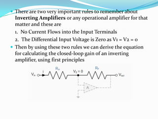
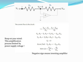
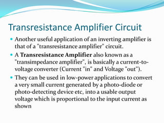
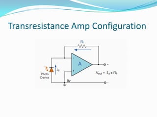
Downloaded 639 times
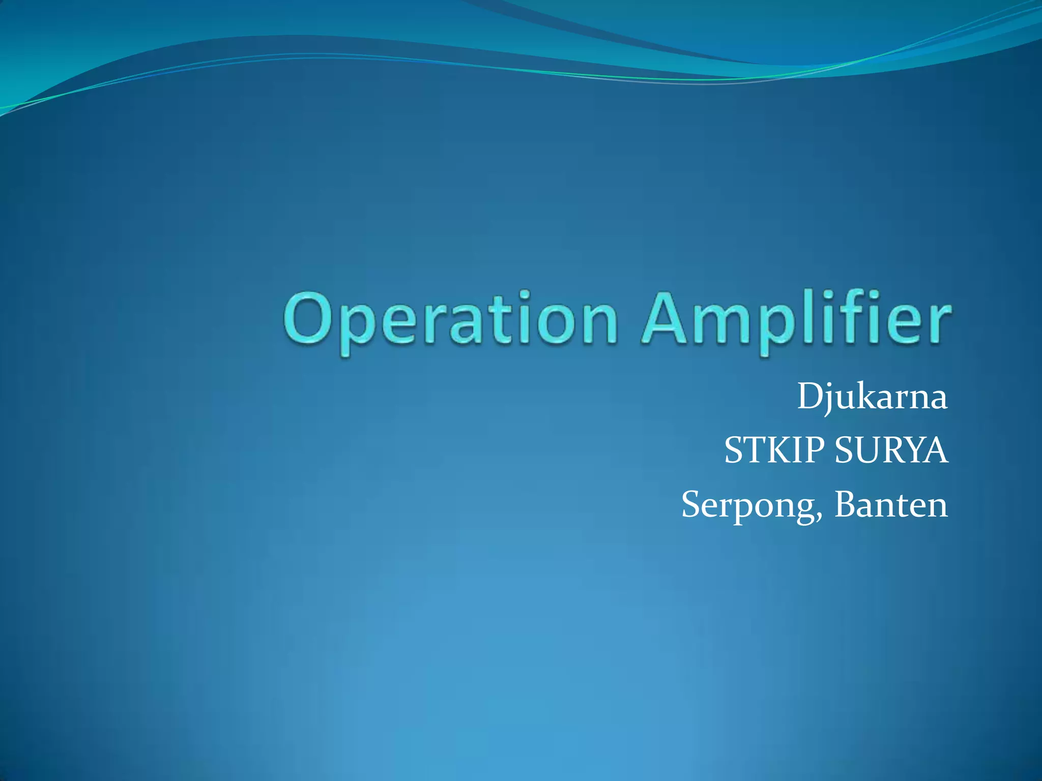
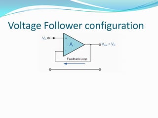
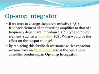
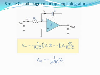
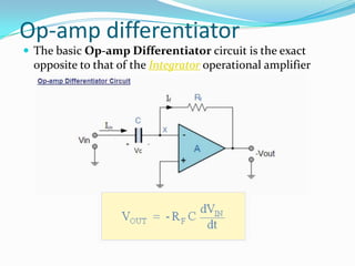
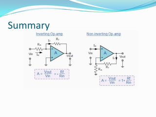
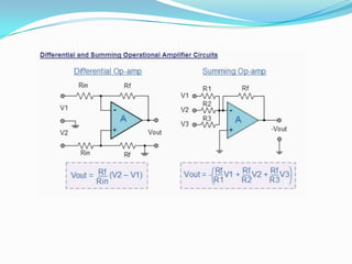
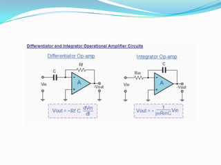

This document provides information on operation amplifiers (op-amps) including their ideal characteristics and common circuit configurations. It describes how op-amps can be used as inverting amplifiers, non-inverting amplifiers, summing amplifiers, differential amplifiers, and integrators/differentiators. Key points covered include the ideal properties of op-amps such as infinite gain and zero input impedance, as well as how negative feedback impacts closed-loop gain. Common applications of each circuit type are also discussed.


