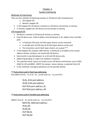
Chapter 6
System Interfacing
Methods of Interfacing
There are two methods of interfacing memory or I/O devices with microprocessor
1. I/O mapped I/O
2. Memory mapped I/O
 In I/O mapped I/O, I/O device is treated as a I/O device and memory as memory.
 In memory mapped I/O, I/O devices are also treated as memory.
I/O mapped I/O
 I/O device is treated as I/O device & memory as memory
 Each I/O device uses either 8 address lines (Fixed port) or 16 address lines ( Variable
port)
 In fixed port 256 input and 256 output devices can be connected
 In variable port, 65,536 input & 65,536 output devices can be used
 The instructions used in both types of ports are as given ***.
 In I/O mapped I/O, complete 1MB memory is interfaced as all address lines used to
address memory locations, not shared with I/O devices.
 Data transfer is possible between AL or AX and I/O devices only.
 Addressing decoding is simple, less hardware is required.
 The separate control signals are used to access I/O devices and memory such as IORC,
IOWC for I/O and MRDC , MWTC for memory. Hence memory is protected from I/O.
 In I/O, arithmetic and logical operations are not possible directly
***Instructions used in Fixed type addressing
Any address line A0 - A7 or A8 – A15 can be used. A16 - A19 are all 0’s.
INAL, 8 bit portaddress
INAX, 8 bit portaddress
OUT 8 bit port address, AL
OUT 8 bit port address, AX
***Instructions used in Variable type addressing
Address lines A0 - A15 are be used. A16 - A19 are all 0’s.
MOV DX, 16bit portaddress
INAL,DX
INAX,DX
OUT DX,AL
OUT DX,AX
Memory Mapped I/O
 In this technique, i/o devices are treated as memory and memory as memory, hence the
address of the i/o devices are same as memory addresses (20-bit)
 So, the addresses of I/O and memory are shared
 All 20 address lines are used for i/o and memory.
 The same control signals MRDC MWTC are used both for i/o and memory
 Data transfer is possible between any register unlike in i/o mapped i/o.
 All memory related instructions are used for i/o operations
 Address decoding of the i/o devices and memory devices are complicated and
expensive.
 Total no. of i/o ports and memory cannot be more than 1MB
 Looping techniques can be used to access more no. of i/o devices
 i/o devices and memory devices are differentiated by their addresses only, in all other
cases they are treated the same.
 Since memory instructions take long time to execute, speed of memory mapped i/o
logic circuits are less.
Differences between i/o mapped i/o and memory mapped i/o :
Sr.
No.
I/O mapped I/O Memory mapped I/O
1. I/O device is treated as I/O device &
memory as memory
i/o devices and memory both are treated as
memory
2 The separate control signals are used to
access I/O devices and memory such as
IORC, IOWC for I/O and MRDC , MWTC
for memory.
The same control signals MRDC MWTC are
used both for i/o and memory
3 IN and OUT instructions are used for i/o
read and write operations
All memory read and write instructions are
used
4 Addressing decoding is simple, less
hardware is required.
Address decoding of the i/o devices and
memory devices are complicated and
expensive.
5 64K of Input, 64K of output, 1MB of
memory can be used
1MB of memory is shared between i/o and
memory
6 Device addresses can be either 8 or 16
bits
20-bit addressing is used for both i/o and
memory
7 i/o and memory are distinguished with
the help of control signals and
addresses.
Cannot be distinguished using control signals,
can be distinguished only using addresses
8 arithmetic and logical operations are
not possible directly
arithmetic and logical operations are possible
directly with i/o devices
9 Data transfer is possible between AL or
AX and I/O devices only.
Data transfer is possible between any register
and i/o devices.
10. Slower in execution Since memory instructions take long time to
execute, speed of memory mapped i/o logic
circuits are less.
Memory Interfacing :--
Interfacing memory with Odd and even memory banks :--
The figure below shows the interfacing of the memory with odd and even memory
banks. A0 signal is used to indicate that the chip selected is even bank and BHE signal is used to
indicate that the ship selected is odd memory.
The figure below shows a 2716 EPROMchip used to interface with microprocessor. It has 11
address lines which are given from the microprocessor directly. Other lines on the
microprocessor are used to interface the chips (chip select lines).
Interfacing two 2K EPROM :--
 Address line A0 for even memory bank
 BHE for odd memory bank
 A1 to A11 for addresses.
 A12 to A19 for chip select, used as the input to a NAND gate
Addressing decoding worksheet for the above diagram is as given below.
Interfacing four 2K X 8 RAM :--
 Address line A0 for even memory bank
 BHE for odd memory bank
 A1 to A11 for addresses.
 A12 to A14 as input signals to 74138 IC so that one out of Y0 to Y7 are used to select the
chip
 A15 to A19 are the gated inputs for enabling 74138.
The address decoding worksheet for the above is as given below.
Example of Interfacing:--
Interface
a) 8K of EPROM (IC 2764) and
b) 8k word RAM (IC 6264) to 8086.
Use block decoding. EPROM address starts at FC000 H and RAM address at 1C000 H
Solution:--
EPROM:--
 No. of address lines – 23 . 210  13 address lines
RAM:--
 No. of address lines - 23 . 210  13 address lines

Notes chapter 6

  • 1.
    Chapter 6 System Interfacing Methodsof Interfacing There are two methods of interfacing memory or I/O devices with microprocessor 1. I/O mapped I/O 2. Memory mapped I/O  In I/O mapped I/O, I/O device is treated as a I/O device and memory as memory.  In memory mapped I/O, I/O devices are also treated as memory. I/O mapped I/O  I/O device is treated as I/O device & memory as memory  Each I/O device uses either 8 address lines (Fixed port) or 16 address lines ( Variable port)  In fixed port 256 input and 256 output devices can be connected  In variable port, 65,536 input & 65,536 output devices can be used  The instructions used in both types of ports are as given ***.  In I/O mapped I/O, complete 1MB memory is interfaced as all address lines used to address memory locations, not shared with I/O devices.  Data transfer is possible between AL or AX and I/O devices only.  Addressing decoding is simple, less hardware is required.  The separate control signals are used to access I/O devices and memory such as IORC, IOWC for I/O and MRDC , MWTC for memory. Hence memory is protected from I/O.  In I/O, arithmetic and logical operations are not possible directly ***Instructions used in Fixed type addressing Any address line A0 - A7 or A8 – A15 can be used. A16 - A19 are all 0’s. INAL, 8 bit portaddress INAX, 8 bit portaddress OUT 8 bit port address, AL OUT 8 bit port address, AX ***Instructions used in Variable type addressing Address lines A0 - A15 are be used. A16 - A19 are all 0’s. MOV DX, 16bit portaddress INAL,DX INAX,DX OUT DX,AL OUT DX,AX
  • 2.
    Memory Mapped I/O In this technique, i/o devices are treated as memory and memory as memory, hence the address of the i/o devices are same as memory addresses (20-bit)  So, the addresses of I/O and memory are shared  All 20 address lines are used for i/o and memory.  The same control signals MRDC MWTC are used both for i/o and memory  Data transfer is possible between any register unlike in i/o mapped i/o.  All memory related instructions are used for i/o operations  Address decoding of the i/o devices and memory devices are complicated and expensive.  Total no. of i/o ports and memory cannot be more than 1MB  Looping techniques can be used to access more no. of i/o devices  i/o devices and memory devices are differentiated by their addresses only, in all other cases they are treated the same.  Since memory instructions take long time to execute, speed of memory mapped i/o logic circuits are less. Differences between i/o mapped i/o and memory mapped i/o : Sr. No. I/O mapped I/O Memory mapped I/O 1. I/O device is treated as I/O device & memory as memory i/o devices and memory both are treated as memory 2 The separate control signals are used to access I/O devices and memory such as IORC, IOWC for I/O and MRDC , MWTC for memory. The same control signals MRDC MWTC are used both for i/o and memory 3 IN and OUT instructions are used for i/o read and write operations All memory read and write instructions are used 4 Addressing decoding is simple, less hardware is required. Address decoding of the i/o devices and memory devices are complicated and expensive. 5 64K of Input, 64K of output, 1MB of memory can be used 1MB of memory is shared between i/o and memory 6 Device addresses can be either 8 or 16 bits 20-bit addressing is used for both i/o and memory 7 i/o and memory are distinguished with the help of control signals and addresses. Cannot be distinguished using control signals, can be distinguished only using addresses 8 arithmetic and logical operations are not possible directly arithmetic and logical operations are possible directly with i/o devices
  • 3.
    9 Data transferis possible between AL or AX and I/O devices only. Data transfer is possible between any register and i/o devices. 10. Slower in execution Since memory instructions take long time to execute, speed of memory mapped i/o logic circuits are less. Memory Interfacing :-- Interfacing memory with Odd and even memory banks :-- The figure below shows the interfacing of the memory with odd and even memory banks. A0 signal is used to indicate that the chip selected is even bank and BHE signal is used to indicate that the ship selected is odd memory.
  • 4.
    The figure belowshows a 2716 EPROMchip used to interface with microprocessor. It has 11 address lines which are given from the microprocessor directly. Other lines on the microprocessor are used to interface the chips (chip select lines). Interfacing two 2K EPROM :--  Address line A0 for even memory bank  BHE for odd memory bank  A1 to A11 for addresses.  A12 to A19 for chip select, used as the input to a NAND gate
  • 5.
    Addressing decoding worksheetfor the above diagram is as given below. Interfacing four 2K X 8 RAM :--  Address line A0 for even memory bank  BHE for odd memory bank  A1 to A11 for addresses.  A12 to A14 as input signals to 74138 IC so that one out of Y0 to Y7 are used to select the chip  A15 to A19 are the gated inputs for enabling 74138.
  • 6.
    The address decodingworksheet for the above is as given below.
  • 7.
    Example of Interfacing:-- Interface a)8K of EPROM (IC 2764) and b) 8k word RAM (IC 6264) to 8086. Use block decoding. EPROM address starts at FC000 H and RAM address at 1C000 H Solution:-- EPROM:--  No. of address lines – 23 . 210  13 address lines RAM:--  No. of address lines - 23 . 210  13 address lines