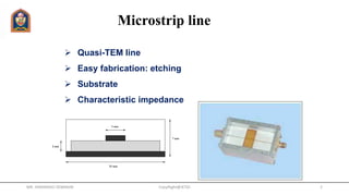
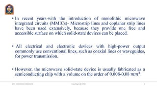
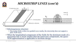
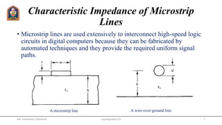
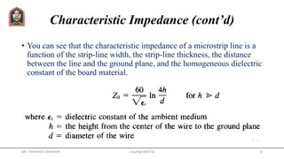
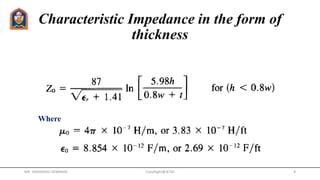
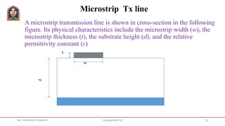
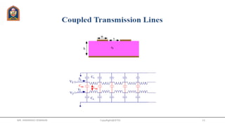
Microstrip transmission
lines
By:- MR. HIMANSHU DIWAKAR
Assistant Professor
JETGI
MR. HIMANSHU DIWAKAR CopyRight@JETGI 1
Microstrip line
 Quasi-TEM line
 Easy fabrication: etching
 Substrate
 Characteristic impedance
CopyRight@JETGI 2
MR. HIMANSHU DIWAKAR
• In recent years-with the introduction of monolithic microwave
integrated circuits (MMICs)- Microstrip lines and coplanar strip lines
have been used extensively, because they provide one free and
accessible surface on which solid-state devices can be placed.
• All electrical and electronic devices with high-power output
commonly use conventional lines, such as coaxial lines or waveguides,
for power transmission.
• However, the microwave solid-state device is usually fabricated as a
semiconducting chip with a volume on the order of 0.008-0.08 𝑚𝑚3.
MR. HIMANSHU DIWAKAR CopyRight@JETGI 3
MICROSTRIP LINES (cont’d)
• Inhomogeneous structure:
• Due to the fields within two guided-wave media, the microstrip does not support a
pure TEM wave.
• When the longitudinal components of the fields for the dominant mode of a
microstrip line is much smaller than the transverse components, the quasi-
TEM approximation is applicable to facilitate design.
MR. HIMANSHU DIWAKAR CopyRight@JETGI 4
MICROSTRIP LINES (cont’d)
• Can be fabricated using PCB technology.
• It consists of a conducting strip separated from a ground plane by a
dielectric known as substrate.
• It’s Components are couplers, filters
• Power divided can formed using microstrip lines
• Less expensive as traditional waveguide technology as well as lighter and
compact.
• Low power handling capacity and higher radiation losses.
• Like waveguide microstrip is not enclosed.
• Microwave integrated circuits with microstrip lines are commonly
• used with the chips. The microstrip line is also called an open-strip line.
MR. HIMANSHU DIWAKAR CopyRight@JETGI 5
• Radiation loss in microstrip lines is a problem, particularly at such
discontinuities as short circuit posts, corners, and so on.
• However, the use of thin, high-dielectric materials considerably
reduces the radiation loss of the open strip.
MR. HIMANSHU DIWAKAR CopyRight@JETGI 6
Characteristic Impedance of Microstrip
Lines
• Microstrip lines are used extensively to interconnect high-speed logic
circuits in digital computers because they can be fabricated by
automated techniques and they provide the required uniform signal
paths.
A microstrip line A wire-over-ground line.
MR. HIMANSHU DIWAKAR CopyRight@JETGI 7
Characteristic Impedance (cont’d)
• You can see that the characteristic impedance of a microstrip line is a
function of the strip-line width, the strip-line thickness, the distance
between the line and the ground plane, and the homogeneous dielectric
constant of the board material.
MR. HIMANSHU DIWAKAR CopyRight@JETGI 8
Characteristic Impedance in the form of
thickness
Where
MR. HIMANSHU DIWAKAR CopyRight@JETGI 9
A microstrip transmission line is shown in cross-section in the following
figure. Its physical characteristics include the microstrip width (w), the
microstrip thickness (t), the substrate height (d), and the relative
permittivity constant (ε)
CopyRight@JETGI 10
d
w
t
Microstrip Tx line
MR. HIMANSHU DIWAKAR
Substrate
  Relative permittivity
 Thickness of a substrate: mil (inch/1000)
 Thickness of a metal: oz (almost 1.4 mils)
 Loss: loss tangent
 Temperature
CopyRight@JETGI 11
MR. HIMANSHU DIWAKAR
Coupled Transmission Lines
• Coupling between two transmission lines is introduced by their
proximity to each other.
• Coupling effects may be undesirable, such as crosstalk in printed
circuits, or they may be desirable, as in directional couplers where the
objective is to transfer power from one line to the other
CopyRight@JETGI 12
MR. HIMANSHU DIWAKAR
CopyRight@JETGI 13
MR. HIMANSHU DIWAKAR
MR. HIMANSHU DIWAKAR CopyRight@JETGI 14
Electrical wall
Even mode Magnetic Wall
Electric field
Magnetic field
Coupled line Structure
The coupled line structure supports two quasi-TEM modes: odd mode and even
mode
Odd mode
Strip lines
• Combination of two wire lines and co-axial lines.
• These are basically planer transmission lines and are widely used for
frequencies from 100 MHz to 100 GHz.
MR. HIMANSHU DIWAKAR CopyRight@JETGI 15
• A Strip line consists of a central thin conducting strip of width ω
which is greater than its thickness t. It is placed inside the low loss
dielectric (εr) substrate of thickness b/2 between two wide ground
plates.
• The width of the ground plates is five times greater than the spacing
between the plates.
• The fundamental and dominant mode in Strip lines is TEM mode.
• For b<λ/2, there will be no propagation in the transverse direction.
MR. HIMANSHU DIWAKAR CopyRight@JETGI 16
Coplanar strip lines
• A Coplanar strip line is formed by two conducting strips with one
strip grounded, both being placed on the same substrate surface, for
convenient connections. The following figure explains this.
MR. HIMANSHU DIWAKAR CopyRight@JETGI 17
MR. HIMANSHU DIWAKAR CopyRight@JETGI 18
CopyRight@JETGI 19
Thank you
MR. HIMANSHU DIWAKAR

microstriptl1st3-170309071044.pdf

  • 1.
    Microstrip transmission lines By:- MR.HIMANSHU DIWAKAR Assistant Professor JETGI MR. HIMANSHU DIWAKAR CopyRight@JETGI 1
  • 2.
    Microstrip line  Quasi-TEMline  Easy fabrication: etching  Substrate  Characteristic impedance CopyRight@JETGI 2 MR. HIMANSHU DIWAKAR
  • 3.
    • In recentyears-with the introduction of monolithic microwave integrated circuits (MMICs)- Microstrip lines and coplanar strip lines have been used extensively, because they provide one free and accessible surface on which solid-state devices can be placed. • All electrical and electronic devices with high-power output commonly use conventional lines, such as coaxial lines or waveguides, for power transmission. • However, the microwave solid-state device is usually fabricated as a semiconducting chip with a volume on the order of 0.008-0.08 𝑚𝑚3. MR. HIMANSHU DIWAKAR CopyRight@JETGI 3
  • 4.
    MICROSTRIP LINES (cont’d) •Inhomogeneous structure: • Due to the fields within two guided-wave media, the microstrip does not support a pure TEM wave. • When the longitudinal components of the fields for the dominant mode of a microstrip line is much smaller than the transverse components, the quasi- TEM approximation is applicable to facilitate design. MR. HIMANSHU DIWAKAR CopyRight@JETGI 4
  • 5.
    MICROSTRIP LINES (cont’d) •Can be fabricated using PCB technology. • It consists of a conducting strip separated from a ground plane by a dielectric known as substrate. • It’s Components are couplers, filters • Power divided can formed using microstrip lines • Less expensive as traditional waveguide technology as well as lighter and compact. • Low power handling capacity and higher radiation losses. • Like waveguide microstrip is not enclosed. • Microwave integrated circuits with microstrip lines are commonly • used with the chips. The microstrip line is also called an open-strip line. MR. HIMANSHU DIWAKAR CopyRight@JETGI 5
  • 6.
    • Radiation lossin microstrip lines is a problem, particularly at such discontinuities as short circuit posts, corners, and so on. • However, the use of thin, high-dielectric materials considerably reduces the radiation loss of the open strip. MR. HIMANSHU DIWAKAR CopyRight@JETGI 6
  • 7.
    Characteristic Impedance ofMicrostrip Lines • Microstrip lines are used extensively to interconnect high-speed logic circuits in digital computers because they can be fabricated by automated techniques and they provide the required uniform signal paths. A microstrip line A wire-over-ground line. MR. HIMANSHU DIWAKAR CopyRight@JETGI 7
  • 8.
    Characteristic Impedance (cont’d) •You can see that the characteristic impedance of a microstrip line is a function of the strip-line width, the strip-line thickness, the distance between the line and the ground plane, and the homogeneous dielectric constant of the board material. MR. HIMANSHU DIWAKAR CopyRight@JETGI 8
  • 9.
    Characteristic Impedance inthe form of thickness Where MR. HIMANSHU DIWAKAR CopyRight@JETGI 9
  • 10.
    A microstrip transmissionline is shown in cross-section in the following figure. Its physical characteristics include the microstrip width (w), the microstrip thickness (t), the substrate height (d), and the relative permittivity constant (ε) CopyRight@JETGI 10 d w t Microstrip Tx line MR. HIMANSHU DIWAKAR
  • 11.
    Substrate   Relativepermittivity  Thickness of a substrate: mil (inch/1000)  Thickness of a metal: oz (almost 1.4 mils)  Loss: loss tangent  Temperature CopyRight@JETGI 11 MR. HIMANSHU DIWAKAR
  • 12.
    Coupled Transmission Lines •Coupling between two transmission lines is introduced by their proximity to each other. • Coupling effects may be undesirable, such as crosstalk in printed circuits, or they may be desirable, as in directional couplers where the objective is to transfer power from one line to the other CopyRight@JETGI 12 MR. HIMANSHU DIWAKAR
  • 13.
  • 14.
    MR. HIMANSHU DIWAKARCopyRight@JETGI 14 Electrical wall Even mode Magnetic Wall Electric field Magnetic field Coupled line Structure The coupled line structure supports two quasi-TEM modes: odd mode and even mode Odd mode
  • 15.
    Strip lines • Combinationof two wire lines and co-axial lines. • These are basically planer transmission lines and are widely used for frequencies from 100 MHz to 100 GHz. MR. HIMANSHU DIWAKAR CopyRight@JETGI 15
  • 16.
    • A Stripline consists of a central thin conducting strip of width ω which is greater than its thickness t. It is placed inside the low loss dielectric (εr) substrate of thickness b/2 between two wide ground plates. • The width of the ground plates is five times greater than the spacing between the plates. • The fundamental and dominant mode in Strip lines is TEM mode. • For b<λ/2, there will be no propagation in the transverse direction. MR. HIMANSHU DIWAKAR CopyRight@JETGI 16
  • 17.
    Coplanar strip lines •A Coplanar strip line is formed by two conducting strips with one strip grounded, both being placed on the same substrate surface, for convenient connections. The following figure explains this. MR. HIMANSHU DIWAKAR CopyRight@JETGI 17
  • 18.
    MR. HIMANSHU DIWAKARCopyRight@JETGI 18
  • 19.