Download to read offline

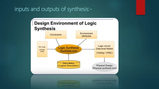
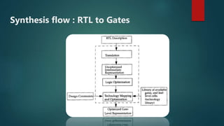
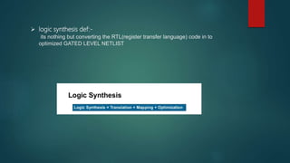
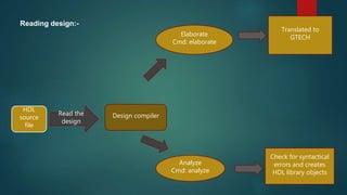
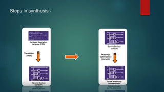
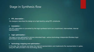


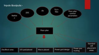
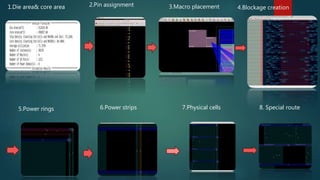

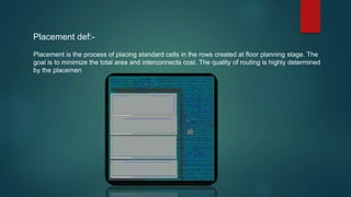
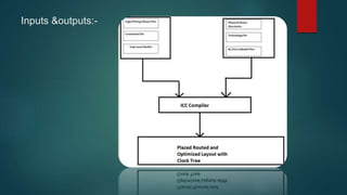


The document discusses the steps in the logic synthesis process from RTL to optimized gate-level netlist. It includes: 1) RTL description is converted to an internal representation 2) Logic is optimized to remove redundancy 3) Technology mapping implements the representation using cells from a technology library The document also discusses floor planning, which determines routing areas by placing blocks/macros, and placement which places standard cells in rows to minimize area and interconnect cost.