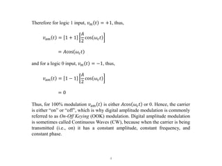
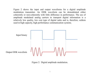
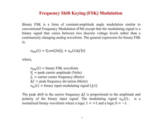
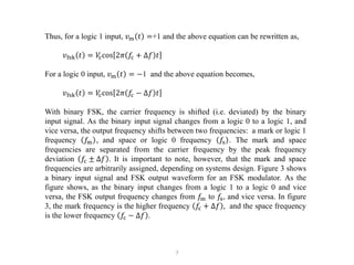
EEEC6440315 COMMUNICATION SYSTEMS
Digital Modulation
FACULTY OF ENGINEERING AND COMPUTER TECHNOLOGY
BENG (HONS) IN ELECTRICALAND ELECTRONIC ENGINEERING
Ravandran Muttiah BEng (Hons) MSc MIET
1
Digital Radio
The property that distinguishes a digital radio system from a conventional
Amplitude Modulation (AM), Frequency Modulation (FM), or Phase
Modulation (PM) radio system is the nature of the modulating signal. Both
digital and analog radio systems use analog carriers; however, with analog
modulation, the modulating signal is analog, and with digital modulation,
the modulating signal is digital. However, that with both analog and digital
modulation, the original source information could have been either analog
or digital.
Figure 1 shows a simplified block diagram for a digital radio system. In the
transmitter, the precoder performs level conversion then encodes or groups
the incoming data into a control word that modulates the analog carrier. The
modulated carrier is shaped (i.e. filtered), amplified, then transmitted
through the transmission medium to the receiver. In the receiver, the
incoming signal is filtered, amplified, and then applied to the demodulator
circuit which reproduces the original source information. Clock and carrier-
recovery circuits remove carrier and clock timing information from the
incoming signal.
2
Precoder Modulator
Bandpass
Filter and
Power
Amplifier
Buffer
Analog
Carrier
Clock
Input
Data
Figure 1: Digital radio system.
Bandpass
Filter and
Amplifier
Demodulator
and Decoder
Bandpass
Filter
Carrier and
Clock
Recovery
Noise
Transmitter Receiver
Transmission
Media
Output
Data
3
Digital Amplitude Modulation
The simplest digital modulation technique is digital amplitude modulation,
which is simply double sideband, full carrier amplitude modulation where
the input modulating signal is a binary waveform. Mathematically, digital
amplitude modulation by a binary signal is,
𝑣am 𝑡 = 1 + 𝑣m 𝑡
𝐴
2
cos 𝜔c𝑡
where,
𝑣am 𝑡 = digital amplitude modulated wave
𝐴
2
= unmodulated carrier amplitude (volts)
𝑣m 𝑡 = modulated binary signal (volts)
𝜔c = carrier radian frequency (radians per second)
The modulating signal 𝑣am 𝑡 is a normalised binary waveform, where
+ 1V = logic 1 and −1V = logic 0.
4
Therefore for logic 1 input, 𝑣m 𝑡 = +1, thus,
𝑣am 𝑡 = 1 + 1
𝐴
2
cos 𝜔c𝑡
= 𝐴cos 𝜔c𝑡
and for a logic 0 input, 𝑣m 𝑡 = −1, thus,
𝑣am 𝑡 = 1 − 1
𝐴
2
cos 𝜔c𝑡
= 0
Thus, for 100% modulation 𝑣am 𝑡 is either 𝐴cos 𝜔c𝑡 or 0. Hence, the carrier
is either “on” or “off”, which is why digital amplitude modulation is commonly
referred to as On-Off Keying (OOK) modulation. Digital amplitude modulation
is sometimes called Continuous Waves (CW), because when the carrier is being
transmitted (i.e., on) it has a constant amplitude, constant frequency, and
constant phase.
5
Figure 2 shows the input and output waveforms for a digital amplitude
modulation transmitter. An OOK waveform can be demodulated either
coherently or non-coherently with little difference in performance. The use of
amplitude modulated analog carriers to transport digital information is a
relatively low quality, low cost type of digital radio and is, therefore, seldom
used in high capacity, high performance communication systems.
Figure 2: Digital amplitude modulation.
Input binary
Output OOK waveform
6
Frequency Shift Keying (FSK) Modulation
Binary FSK is a form of constant-amplitude angle modulation similar to
conventional Frequency Modulation (FM) except that the modulating signal is a
binary signal that varies between two discrete voltage levels rather than a
continuously changing analog waveform. The general expression for binary FSK
is,
𝑣fsk 𝑡 = 𝑉
ccos 2𝜋 𝑓c + 𝑣m 𝑡 ∆𝑓 𝑡
where,
𝑣fsk 𝑡 = binary FSK waveform
𝑉
c = peak carrier amplitude (Volts)
𝑓c = carrier center frequency (Hertz)
∆𝑓 = peak frequency deviation (Hertz)
𝑣m 𝑡 = binary input modulating signal ±1
The peak shift in the carrier frequency ∆𝑓 is proportional to the amplitude and
polarity of the binary input signal. The modulating signal 𝑣m 𝑡 , is a
normalised binary waveform where a logic 1 = +1 and a logic 0 = −1 .
7
Thus, for a logic 1 input, 𝑣m 𝑡 =+1 and the above equation can be rewritten as,
𝑣fsk 𝑡 = 𝑉
ccos 2𝜋 𝑓c + ∆𝑓 𝑡
For a logic 0 input, 𝑣m 𝑡 = −1 and the above equation becomes,
𝑣fsk 𝑡 = 𝑉
ccos 2𝜋 𝑓c − ∆𝑓 𝑡
With binary FSK, the carrier frequency is shifted (i.e. deviated) by the binary
input signal. As the binary input signal changes from a logic 0 to a logic 1, and
vice versa, the output frequency shifts between two frequencies: a mark or logic 1
frequency 𝑓m , and space or logic 0 frequency 𝑓s . The mark and space
frequencies are separated from the carrier frequency by the peak frequency
deviation 𝑓c ± ∆𝑓 . It is important to note, however, that the mark and space
frequencies are arbitrarily assigned, depending on systems design. Figure 3 shows
a binary input signal and FSK output waveform for an FSK modulator. As the
figure shows, as the binary input changes from a logic 1 to a logic 0 and vice
versa, the FSK output frequency changes from 𝑓m to 𝑓s, and vice versa. In figure
3, the mark frequency is the higher frequency 𝑓c + ∆𝑓 , and the space frequency
is the lower frequency 𝑓c − ∆𝑓 .
8
Binary Input Analog Output
1 0 1 0 1 0
Input
Output
𝑓 =
𝑓b
4
𝑓m
𝑡b 𝑡b 𝑡b 𝑡b 𝑡b 𝑡b
1 1 0 0 0 1
𝑡b 𝑡b 𝑡b 𝑡b 𝑡b 𝑡b
0
𝑓s 𝑓m 𝑓s 𝑓m 𝑓s 𝑓s 𝑓m 𝑓m 𝑓s 𝑓s 𝑓s 𝑓m
𝑓 =
𝑓b
2
2𝑇1
𝑇1
𝑡b
0
𝑓s
Figure 3: Binary FSK input and output waveforms.
FSK Modulator
(VCO)
9
FSK Bit Rate And Baud
With binary FSK, there is a change in the output frequency each time the
logic condition of the binary input signal changes. Consequently, the output
rate of change is equal to the input rate of change. In digital modulation, the
rate of change at the input to the modulator is called the bit rate 𝑓b and
has the unit of bits per second (bps). The rate of change at the output of the
modulator is called baud, after J. M. E. Baudot.
Baud is often misunderstood and commonly confused with bit rate. Baud is
a rate of change and is equal to the reciprocal of the time of one output
signaling element. With FSK, the time of an output signaling element is the
minimum time either the mark or space frequency is outputted, which is
equal to the time of a single bit 𝑡b . As shown in figure 3, the output
changes from a mark frequency to a space frequency and vice versa at the
same rate that the input condition changes from logic 1 to a logic 0 and vice
versa. The minimum time that a mark frequency can be outputted equals the
time of one bit. Therefore, with binary FSK, the time of a signaling element
and the time of a bit rate are equal; thus, the input and output rates of
change are equal and the bit rate and baud must also be equal.
10
Bandwidth Considerations Of FSK
The output of a FSK modulator is related to the binary input as shown in
figure 4 where a logic 0 corresponds to space frequency 𝑓s, a logic 1
corresponds to the mark frequency 𝑓m, and 𝑓c is the carrier frequency. The
peak frequency deviation is,
∆𝑓 =
𝑓m − 𝑓s
2
The FSK consists of two pulsed sinusoidal waves of frequency 𝑓m and 𝑓s
which have frequency spectrums that are
sin 𝑥
𝑥
functions. The peaks of the
power spectrum contain the bulk of the energy, the minimum bandwidth is,
𝐵𝑊 = 𝑓s + 𝑓b − 𝑓m − 𝑓b
= 𝑓s − 𝑓m + 2𝑓b
Since 𝑓s − 𝑓m equals 2∆𝑓, the minimum bandwidth can be approximated as,
𝐵𝑊 = 2∆𝑓 + 2𝑓b
= 2 ∆𝑓 + 𝑓b
11
NRZ Binary Input FSK Output
FSK Modulator
0 1 0 1
𝑡b 𝑓
m 𝑓
s
𝑓
c
𝑓
m 𝑓
s
𝑓
c
𝐵𝑊
𝑓m −
1
𝑡b
𝑓
s +
1
𝑡b
Figure 4: FSK frequency spectrum.
𝑓
c − ∆𝑓 𝑓
c + ∆𝑓
𝐵𝑊
12
Example 1:
Determine (a) the peak frequency deviation, (b) the minimum bandwidth, and
(c) baud for an FSK signal with a mark frequency of 49 KHz, a space
frequency of 51 KHz, and an input bit rate of 2 Kbps.
Solution:
(a) The peak frequency deviation is found by substituting into the following
equation,
∆𝑓c =
𝑓m − 𝑓s
2
=
49 KHz − 51 KHz
2
= 1 KHz
(b) The minimum bandwidth is found by substituting into the following
equation,
𝐵 = 2 ∆𝑓 + 𝑓𝑏 = 2 1000 + 2000 = 6 KHz
(c) With FSK, the baud is equal to the bit rate, 2000.
13
Binary Phase Shift Keying (BPSK) Modulation
With BPSK Modulation, two output phases are possible for a single carrier
frequency (binary meaning ‘2’). One output phase represents a logic 1 and
the other a logic 0. As the input digital signal changes state, the phase of the
output carrier shifts between two angle that are out of phase. BPSK is a
form of suppressed-carrier, squarewave modulation of a continuous wave
(CW) signal. Figure 5 shows a simplified block diagram of a BPSK
modulation process.
Binary Data
Input
Modulated
PSK Output
Reference Carrier Signal
Figure 5: BPSK modulator.
BPSK Modulator
Figure 6 shows the truth table, phasor diagram and constellation diagram for a BPSK
modulator.
Binary input Output phase
Logic 0
Logic 1
Figure 6(a): Truth table.
Logic 1
Logic 0
Figure 6(b): Phasor diagram.
14
+90°
cos 𝜔c𝑡
−cos 𝜔c𝑡
−90°
−sin 𝜔c𝑡
180°
sin 𝜔c𝑡
0°
0°
180°
Logic 1
Logic 0
Figure 6(c): Constellation diagram.
15
cos 𝜔c𝑡
−cos 𝜔c𝑡
±180°
0°
1 0 1 0 1 0
Binary Input
BPSK Output
Time
Time
sin𝜔c𝑡
Figure 7: Output versus time for a BPSK modulator.
sin𝜔c𝑡 sin𝜔c𝑡
−sin𝜔c𝑡 −sin𝜔c𝑡 −sin𝜔c𝑡
0 180 180 180
0 0
0 0 0
π π π
𝑡b 𝑡b 𝑡b 𝑡b 𝑡b 𝑡b
16
Level converter
(UP to BP)
Balanced
Modulator
Bandpass
Filter
Buffer
Reference
Carrier Oscillator
Modulated
PSK output
Binary Data
Input
+𝑉
−𝑉
+𝑉
0
Figure 8: BPSK transmitter.
17
Balanced
Modulator
Bandpass
Filter
Lowpass
Filter
Level
Converter
Coherent
Carrier
Recovery
Clock
Recovery
BPSK
Input
UP Binary
Data Output
+𝑉
0
Figure 9: BPSK receiver.
±sin 𝜔c𝑡
±sin 𝜔c𝑡
The output spectrum from a BPSK modulator is simply a double sideband, suppressed
carrier signal where the upper and lower side frequencies are separated from the carrier
frequency by a value equal to one half the bit rate. Consequently, the minimum
bandwidth 𝑓N required to pass the worst-case BPSK output signal is equal to the input
bit rate.
18
19
Example 2:
For a BPSK modulator with a carrier frequency of 70 MHz and an input bit rate of
10 Mbps, determine the maximum and minimum upper and lower side frequencies,
draw the output spectrum, determine the minimum Nyquist bandwidth, and
calculate the baud.
Solution:
Substituting into the following equation yields,
Output = sin 𝜔a𝑡 sin 𝜔c𝑡
= sin 2π 5 MHz 𝑡 sin 2π 70 MHz 𝑡
=
1
2
cos 2π 70 MHz − 5 MHz 𝑡 −
1
2
cos 2π 70 MHz + 5 MHz 𝑡
Lower side frequency Upper side frequency
20
Minimum lower side frequency, LSF = 70 MHz − 5 MHz = 65 MHz
Maximum upper side frequency, USF = 70 MHz + 5 MHz = 75 MHz
Therefore, the output spectrum for the worst case binary input conditions is as
follows:
The minimum Nyquist bandwidth, 𝑓N = 75 MHz − 65 MHz = 10 MHz
and the baud = 𝑓b or 10 Megabaud.
𝐵𝑊 = 10 MHz
65 MHz 70 MHz 75 MHz
(Suppressed)
A balanced modulator is a product modulator; the output signal is the product of
the two input signals. In a BPSK modulator, the carrier input signal is multiplied
by the binary data. If +1 V is assigned to a logic 1 and −1 V is assigned to a
logic 0, the input carrier sin 𝜔c𝑡 is multiplied by either a + or −1 .
Consequently, the output signal is either +1 sin𝜔c𝑡 or −1 sin𝜔c𝑡 ; the first
represents a signal that is in phase with the reference oscillator, the latter a signal
that is 180°
out of phase with the reference oscillator. Each time the input logic
condition changes, the output phase changes. Consequently, for BPSK, the output
rate change (baud) is equal to the input rate of change (bps), and the widest
output bandwidth occurs when the input binary data are a alternating 1/0
sequence. The fundamental frequency 𝑓a of an alternative 1/0 bit sequence is
equal to one-half of the bit rate 𝑓a/2 . Mathematically, the output of a BPSK
modulator is proportional to,
BPSK output = sin 2π𝑓a𝑡 × sin 2π𝑓c𝑡
where,
𝑓a = maximum fundamental frequency of binary input (Hertz)
𝑓c = reference carrier frequency (Hertz)
Bandwidth Considerations Of BPSK
21
Solving for the trig identity for the product of two sine functions,
1
2
cos 2π 𝑓c − 𝑓a 𝑡 −
1
2
cos 𝑓c + 𝑓a 𝑡
Thus, the minimum double-sided Nyquist bandwidth 𝐹N is,
𝑓c + 𝑓a 𝑓c + 𝑓a
− 𝑓c+𝑓a
2𝑓a
or
−𝑓c+𝑓a
2𝑓a
and because 𝑓a =
𝑓b
2
where 𝑓b = input bit rate,
𝐵𝑊 =
2𝑓b
2
= 𝑓b
where 𝐵𝑊 is the minimum double-sided Nyquist bandwidth.
22
23
Differential Binary Phase Shift Keying (DBPSK)
DBPSK is an alternative form of digital modulation where the
binary input information is contained in the difference between two
successive signaling elements rather than the absolute phase. With
DBPSK it is not necessary to recover a phase-coherent carrier.
Instead, a received signaling element is delayed by one signaling
element time slot and then compared with the next received
signaling element. The difference in the phase of the two signaling
elements determines the logic condition of the data.
24
DBPSK Transmitter
Figure 10(a) shows a simplified DBPSK transmitter. An incoming
information bit is XNORed with the preceding bit prior to entering the
BPSK modulator (i.e. balanced modulator). For the first data bit, there
is no preceding bit with which to compare it. Therefore, an initial
reference bit is assumed. Figure 10(b) shows the relationship between
the input data, the XNOR output data, and the phase at the output of the
balanced modulator. If the initial reference bit is assumed a logic 1, the
output from the XNOR circuit is simply the complement of that shown.
The first data bit is XNORed with the reference bit. If they are the same,
the XNOR output is a logic 1; if they are different, the XNOR output is
a logic 0. The balanced modulator operates the same as a conventional
BPSK modulator; a logic 1 produces + sin 𝜔c𝑡 at the output and a logic
0 produces − sin 𝜔c𝑡 at the output.
25
DBPSK Receiver
Figure 11(a) shows the block diagram and timing sequence for a
DBPSK receiver. The received signal is delayed by one bit time, then
compared with the next signaling element in the balanced modulator. If
they are the same, a logic 1 (+ voltage) is generated. If they are
different, a logic 0 (− voltage) is generated. If the reference phase is
incorrectly assumed, only the first demodulated bit is in error.
Differential encoding can be implemented with higher-than-binary
digital modulation schemes, although the differential algorithms are
much more complicated than for DBPSK.
The primary advantage of DBPSK is the simplicity with which it can be
implemented. With DBPSK, no carrier recovery circuit is needed. A
disadvantage of DBPSK is that it requires between 1dB and 3dB more
signal-to-noise ratio to achieve the same bit error rate as that of absolute
PSK.
26
Balanced
Modulator
1-bit
delay
Data
Input DBPSK
Output
sin 𝜔c𝑡
Input
Data
XNOR
Output
Output
Phase
1 0 0
1
1 0
1 0 1 1 0 1
0 1 1
1 0
1 0 0 0 1 1
1
180°
0°
0°
0
0°
0°
180° 0°
180° 180° 180°
0°
0°
(a)
(b)
Figure 10: DBPSK modulator.
(Reference Bit)
27
Balanced
Modulator
1-bit
delay
DBPSK
Input
Recovered
Data
Balanced modulator output
+ sin 𝜔c𝑡 + sin 𝜔c𝑡 = +
1
2
−
1
2
cos 2𝜔c𝑡
− sin 𝜔c𝑡 − sin 𝜔c𝑡 = +
1
2
−
1
2
cos 2𝜔c𝑡
− sin 𝜔c𝑡 + sin 𝜔c𝑡 = −
1
2
+
1
2
cos 2𝜔c𝑡
(a)
DBPSK
Input
Phase
Recovered
Bit Stream 1 0 0
1
1 0
1 0 1 1 0 1
180°
0°
0° 0°
0°
180° 0°
180° 180° 180°
0°
0°
(Reference Phase)
(b)
Figure 11: DBPSK demodulator.
28
M-Ary Encoding
M is simply a digit that represents the number of conditions or
combinations possible for a given number of binary variables. Binary
FSK and BPSK are M-ary systems where 𝑀 = 2. With PSK system
with four possible output phases 𝑀 = 4. If there are eight possible
output phases, 𝑀 = 8, and so on. The number of output conditions,
𝑁 = log2 𝑀
where,
𝑁 = number of bits encoded
𝑀 = number of output conditions possible with 𝑁 bits
With binary FSK each input bit acts independently on the carrier,
producing one of two possible output frequencies.
29
Thus,
𝑁 = log2 2
2𝑁
= 2
converting to logs and solving for 𝑁,
log 2𝑁
= log 2
𝑁 log 2 = log 2
𝑁 =
log 2
log 2
𝑁 = 1
With BPSK, each input bit also independently acts on the carrier,
therefore 𝑁 = 1. If two bits are inputted, encoded together, and then
allowed to simultaneously modulate a carrier, the number of output
condition is,
𝑀 = 22
= 4
30
The minimum bandwidth necessary to pass M-ary digitally modulated
carriers other than FSK (i.e. PSK) can be expressed as,
𝐵𝑊 =
𝑓b
log2 𝑀
where,
𝑓b = input bit rate (bits per second)
If N is substituted for log2 𝑀, then,
𝐵𝑊 =
𝑓b
𝑁
For M-ary PSK the absolute minimum system bandwidth is equal to the
input bit rate divided by the number of bits encoded or grouped together.
31
Quaternary Phase Shift Keying (QPSK) Modulation
Quaternary phase shift keying (QPSK), or quadrature PSK as it is
sometimes called, is another form of angle-modulated, constant-
amplitude digital modulation. QPSK is an 𝑀-ary encoding technique
where 𝑀 = 4 (hence the name “quaternary”, meaning “4”). With QPSK
four output phases are possible for a single carrier frequency. Because
there are four different output phases, there must be four different input
conditions. Because the digital input to a QPSK modulator is a binary
(base 2) signal, to produce four different input conditions, it takes more
than a single input bit. With two bits, there are four possible conditions:
00, 01, 10, and 11. Therefore, with QPSK, the binary input data are
combined into groups of two bits called dibits. Each dibit code generates
one of the four possible output phases. Therefore, for each two-bit dibit
clocked into the modulator, a single output changes occurs. Therefore,
the rate of change at the output (baud rate) is one-half of the input bit
rate.
32
QPSK Transmitter
A block diagram of a QPSK modulator is shown in figure 12. Two bits (a
dibit) are clocked into the bit splitter. After both bits have been serially
inputted, they are simultaneously parallel outputted. One bit is directed
to the I channel and the other to the Q channel. The I bit modulates a
carrier that is in phase with the reference oscillator (hence, the name “I”
for “in phase” channel), and the Q bit modulates a carrier that is 90°
out
of phase or in quadrature with the reference carrier (hence, the name “Q”
for “quadrature” channel).
It can be seen that once a dibit has been split into the I and Q channels,
the operation is the same as in a BPSK modulator. Essentially, a QPSK
modulator is two BPSK modulators combined in parallel. Again, for a
logic 1 = +1 V and a logic 0 = −1 V, two phases are possible at the
output of the I balanced modulator (+ sin 𝜔c𝑡 and − sin 𝜔c𝑡), and two
phases are possible at the output of the Q balanced modulator (+ cos 𝜔c𝑡
and − cos 𝜔c𝑡). When the linear summer combines the two quadrature
(90°
out of phase) signals, there are four possible resultant phasors given
by these expressions: + sin 𝜔c𝑡 + cos 𝜔c𝑡 , + sin 𝜔c𝑡 − cos 𝜔c𝑡 ,
− sin 𝜔c𝑡 + cos 𝜔c𝑡, and − sin 𝜔c𝑡 − cos 𝜔c𝑡.
33
Balanced
Modulator
Balanced
Modulator
90° Phase
Shift
Reference
Carrier
Oscillator
sin 𝜔c𝑡
Bandpass
Filter
Linear
Summer
Bandpass
Filter
Bandpass
Filter
Bit
Splitter
÷ 2
Figure 12: QPSK modulator.
I
Q
sin 𝜔c𝑡
±sin 𝜔c𝑡
±cos 𝜔c𝑡
cos 𝜔c𝑡
QPSK
Output
Binary
Input
Data 𝑓b
Bit
Clock
I Channel
𝑓b
2
Q Channel
𝑓b
2
Logic 1 = +1 V
Logic 0 = −1 V
Logic 1 = +1 V
Logic 0 = −1 V
34
In figure 13 and 14 it can be seen that with QPSK each of the four
possible output phasors has exactly the same amplitude. Therefore, the
binary information must be encoded entirely in the phase of the output
signal. This constant amplitude characteristic is the most important
characteristic of PSK that distinguishes it from Quadrature Amplitude
Modulation (QAM). Also from figure 13 it can be seen that the angular
separation between any two adjacent phasors in QPSK is 90°
. Therefore,
a QPSK signal can undergo almost a +45°
or −45°
shift in phase during
transmission and still retain the correct encoded information when
demodulated at the receiver. Figure 15 shows the output phase-versus-
time relationship for a QPSK modulator.
Binary Input QPSK
Q I Output Phase
0 0 −𝟏𝟑𝟓°
0 1 −𝟒𝟓°
1 0 +𝟏𝟑𝟓°
1 1 +𝟒𝟓°
Table 1: Truth table.
35
cos 𝜔c 𝑡
−cos 𝜔c 𝑡
sin 𝜔c 𝑡
0°
reference
−sin 𝜔c 𝑡
Q I
cos 𝜔c 𝑡 + sin 𝜔c𝑡
1 1
sin 𝜔c𝑡 + 45°
Q I
−cos 𝜔c 𝑡 + sin 𝜔c𝑡
0 1
sin 𝜔c𝑡 − 45°
Q I
−cos 𝜔c 𝑡 − sin 𝜔c𝑡
0 0
sin 𝜔c𝑡 − 135°
Q I
cos 𝜔c 𝑡 − sin 𝜔c𝑡
1 0
sin 𝜔c𝑡 + 135°
cos 𝜔c 𝑡
−cos 𝜔c 𝑡
sin 𝜔c 𝑡
−sin 𝜔c 𝑡
10 •
00 •
•11
• 01
Figure 13: Phasor diagram. Figure 14: Constellation diagram.
36
Figure 15: Output phase-versus-time relationship for a QPSK modulator.
Time
Dibit
Input
QPSK
Output
Phase
Q I
1 0
Q I
0 1
Q I
1 1
Q I
0 0
+135°
−45° +45° −135°
Degrees
37
Bandwidth Considerations Of QPSK
With QPSK, because the input data are divided into two channels, the bit
rate in either the I or the Q channel is equal to one-half of the input data
rate (𝑓b 2). Essentially, the bit splitter stretches the I and Q bits to twice
their input bit length. Consequently, the highest fundamental frequency
present at the data input to the I or the Q balanced modulator is equal to
one-fourth of the input data rate (one-half of 𝑓b 2 = 𝑓b 4). As a result,
the output of the I and Q balanced modulators requires a minimum
double-sided Nyquist bandwidth equal to one-half of the incoming bit
rate (𝑓N = twice 𝑓b 4 = 𝑓b 2).
Thus, with QPSK, a bandwidth compression is realized (the minimum
bandwidth is less than the incoming bit rate). Also, because the QPSK
output signal does not change phase until two bits (a dibit) have been
clocked into the bit splitter, the fastest output rate of change (baud) is
also equal to one-half of the input bit rate. As with BPSK, the minimum
bandwidth and the baud are equal. The output of the balanced
modulators can be expressed mathematically as,
ouput = sin 𝜔a𝑡 sin 𝜔c𝑡
38
where,
𝜔a𝑡 = 2π
𝑓b
4
𝑡 and 𝜔c𝑡 = 2π𝑓c𝑡
Thus,
output = sin 2π
𝑓b
4
𝑡 sin 2π𝑓c𝑡
1
2
cos 2π 𝑓c −
𝑓b
4
𝑡 −
1
2
cos 2π 𝑓c +
𝑓b
4
𝑡
The output frequency spectrum extends from 𝑓c +
𝑓b
4
to 𝑓c −
𝑓b
4
and the
minimum bandwidth 𝑓N is,
𝑓c +
𝑓b
4
− 𝑓c −
𝑓b
4
=
2𝑓b
4
=
𝑓b
2
modulating phase unmodulated carrier phase
39
Example 3:
For a Quadrature Phase Shift Keying (QPSK) modulator with an input data
rate, 𝑓b equal to 10 Mbps and a carrier frequency of 70 MHz, determine the
minimum double sided Nyquist bandwidth, 𝑓N and the baud.
Solution:
The bit rate in both the I and Q channels is equal to one half of the
transmission bit rate or,
𝑓bQ = 𝑓bI =
𝑓b
2
=
10 Mbps
2
= 5 Mbps
The highest fundamental frequency presented to either balanced modulator
is,
𝑓a =
𝑓bQ
2
or
𝑓bI
2
=
5 Mbps
2
= 2.5 MHz
40
The output wave from each balanced modulator is,
sin 2π𝑓a𝑡 sin 2π𝑓c𝑡
1
2
cos 2π 𝑓c − 𝑓a 𝑡 −
1
2
cos 2π 𝑓c + 𝑓a 𝑡
1
2
cos 2π 70 − 2.5 MHz 𝑡 −
1
2
cos 2π 70 + 2.5 MHz 𝑡
1
2
cos 2π 67.5 MHz 𝑡 −
1
2
cos 2π 72.5 MHz 𝑡
The minimum Nyquist bandwidth, 𝑓N = 72.5 − 67.5 MHz = 5 MHz
The symbol rate equals the bandwidth, symbol rate = 5 Megabaud
41
The output spectrum is as follows:
It can be seen that for the same input bit rate the minimum bandwidth
required to pass the output of the QPSK modulator is equal to one half of
that required for the BPSK modulator in Example 2.
The minimum bandwidth for the QPSK system in Example 3 can also be
determined by simply substituting into the equation,
𝐵𝑊 =
𝑓b
𝑁
=
10 Mbps
2
= 5 MHz
𝐵𝑊 = 5 MHz
67.5 MHz 70 MHz 72.5 MHz
(Suppressed)
42
Probability Of Error And Bit Error Rate
Probability of error 𝑃 𝑒 and Bit Error Rate (BER) are often used
interchangeably. 𝑃 𝑒 is a theoretical expectation of the BER for a given
system. BER is an empirical record of a system’s actual bit error performance.
If a system has a 𝑃 𝑒 of 10−5
, this means that, you can expect one bit error in
every 100,000 bits transmitted
1
105 =
1
100,000
. If a system has a BER of 10−5
,
this means that in the past there was one bit error for every 100,000 bits
transmitted. A BER is measured, then compared with the expected probability
of error to evaluate a system’s performance.
Probability of error is a function of the carrier-to-noise power ratio (or more
specifically, the average energy per bit-to-noise power density ratio) and the
number of possible encoding conditions used (M-ary). Carrier-to-noise power
ratio is the ratio of the average carrier power (the combined power of the
carrier and its associated sidebands) to the thermal noise power. Carrier power
can be stated in watts or dBm, where,
𝐶 dBm = 10 log
𝐶 watts
0.001
43
Thermal noise power is expressed as,
𝑁 = 𝐾𝑇𝐵 watts
where,
𝐾 = Boltzmann’s proportionality constant (1.38 × 10⁻²³
Joules per Kelvin)
𝑇 = temperature (kelvin: 0 K = −273°
C, room temperature = 290 K)
𝐵 = bandwidth (Hertz)
𝑁 dBm = 10 log
𝐾𝑇𝐵
0.001
Carrier-to-noise power ratio is,
𝐶
𝑁
=
𝐶
𝐾𝑇𝐵
where,
𝐶 = carrier power (watts)
44
𝐶
𝑁
dB = 10 log
𝐶
𝑁
= 𝐶 dBm − 𝑁 dBm
Energy per bit is simply the energy of a single bit of information. Energy per bit is,
𝐸b = 𝐶𝑇b
J
bit
where,
𝑇b = time of a single bit (seconds)
𝐸b dBJ = 10 log 𝐸b
and because 𝑇b =
1
𝑓b
, where 𝑓b is the bit rate in bits per second, 𝐸b can be rewritten
as,
𝐸b =
𝐶
𝑓b
J
bit
45
𝐸b dBJ = 10 log
𝐶
𝑓b
= 10 log 𝐶 − 10 log 𝑓b
Noise power density is the thermal noise power normalised to a 1 Hz bandwidth.
Therefore, Noise power density,
𝑁0 =
𝑁
𝐵
W
Hz
𝑁0 dBm = 10 log
𝑁
0.001
− 10 log 𝐵
= 𝑁 dBm − 10 log 𝐵
From 𝑁 = 𝐾𝑇𝐵 and 𝑁0 =
𝑁
𝐵
W
Hz
yields,
𝑁0 =
𝐾𝑇𝐵
𝐵
= 𝐾𝑇 W
Hz
46
𝑁0 dBm = 10 log
𝐾
0.001
+ 10 log 𝑇
Energy per bit-to-noise power density ratio is,
𝐸b
𝑁0
=
𝐶 𝑓b
𝑁 𝐵
=
𝐶𝐵
𝑁𝑓b
=
𝐶
𝑁
×
𝐵
𝑓b
where,
𝐵
𝑓b
= noise bandwidth-to-bit rate ratio.
𝐸b
𝑁0
dB = 10 log
𝐶
𝑁
+ 10 log
𝐵
𝑓b
= 10 log 𝐸b − 10 log 𝑁0
47
Example 4:
For a QPSK system and the given parameter, determine:
(a) Carrier power in dBm.
(b) Noise power in dBm.
(c) Noise power density in dBm.
(d) Energy per bit in dBJ.
(e) Carrier-to-noise power ratio in dB.
(f)
𝐸b
𝑁0
ratio.
𝐶 = 10−12
W 𝑓b = 60 Kbps
𝑁 = 1.2 × 10⁻¹⁴
W B = 120 KHz
Solution:
(a) The carrier power in dBm is determined by substituting into equation,
𝐶 dBm = 10log
𝐶 watts
0.001
= 10log
10−12
0.001
= −90 dBm
48
(b) The noise power in dBm is determined by substituting into equation,
𝑁 dBm = 10log
𝐾𝑇𝐵
0.001
= 10log
1.2 × 10⁻¹⁴
0.001
= −109.2 dBm
(c) The noise power density is determined by substituting into equation,
𝑁0 dBm = 10log
𝐾
0.001
+ 10 log 𝑇 = −109.2 dBm − 10 log 120 KHz
= −160 dBm
(d) The energy per bit is determined by substituting into equation,
𝐸b dBJ = 10log
𝐶
𝑓b
= 10log
10−12
60 kbps
= −167.8 dBJ
49
(e) The carrier-to-noise power is determined by substituting into equation,
𝐶
𝑁
dB = 10 log
𝐶
𝑁
= 10log
10−12
1.2 × 10−14
= 19.2 dB
(f) The energy per bit-to-noise density ratio is determined by substituting
into equation,
𝐸b
𝑁0
dB = 10 log
𝐶
𝑁
+ 10 log
𝐵
𝑓b
= 19.2 + 10 log
120 KHz
60 Kbps
= 22.2 dB
50
• The effect of distortion, noise and interference is less in a digital
communication system. This is because the disturbance must be large
enough to change the pulse from one state to other.
• Regenerative repeaters can be used at fixed distance along the link, to
identify and regenerate a pulse before it is degraded to an ambiguous state.
• Digital circuits are more reliable and cheaper.
• The hardware implementation is more flexible because of the use of
microprocessor, VLSI chips etc.
• Signal processing functions like encryption, compression can be employed to
maintain the secrecy of the information.
• Error detecting and error correction codes improve the system performance
by reducing the probability of error.
• The different type of signals such as data, telephone, television can be
treated as identical signals in transmission and switching in a digital
communication system.
• Can avoid signal jamming using spread spectrum technique.
Advantages Of Digital Communications
51
Disadvantages Of Digital Communications
• Quantisation error.
• Every signal are not a digital in nature.
• High power consumption.
• The error introduced error due to quantisation process, cannot be
removed. Hence this error possess a problem for digital signals.
• Infinite bandwidth, bandwidth is inversely proportional to the time period
of the pulses.
• As pulse width reduces bandwidth requirement increases.
• For fast switching or fast speed communication, require to reduce the
time period of pulses or increase the frequency of pulses, this calls for
higher and higher bandwidth.
• Difficult transmission.
(1) Paul H. Young, Electronic Communication Techniques, 5th Edition,
Pearson, 2004.
References
52

Lecture Notes: EEEC6440315 Communication Systems - Digital Modulation

  • 1.
    EEEC6440315 COMMUNICATION SYSTEMS DigitalModulation FACULTY OF ENGINEERING AND COMPUTER TECHNOLOGY BENG (HONS) IN ELECTRICALAND ELECTRONIC ENGINEERING Ravandran Muttiah BEng (Hons) MSc MIET
  • 2.
    1 Digital Radio The propertythat distinguishes a digital radio system from a conventional Amplitude Modulation (AM), Frequency Modulation (FM), or Phase Modulation (PM) radio system is the nature of the modulating signal. Both digital and analog radio systems use analog carriers; however, with analog modulation, the modulating signal is analog, and with digital modulation, the modulating signal is digital. However, that with both analog and digital modulation, the original source information could have been either analog or digital. Figure 1 shows a simplified block diagram for a digital radio system. In the transmitter, the precoder performs level conversion then encodes or groups the incoming data into a control word that modulates the analog carrier. The modulated carrier is shaped (i.e. filtered), amplified, then transmitted through the transmission medium to the receiver. In the receiver, the incoming signal is filtered, amplified, and then applied to the demodulator circuit which reproduces the original source information. Clock and carrier- recovery circuits remove carrier and clock timing information from the incoming signal.
  • 3.
    2 Precoder Modulator Bandpass Filter and Power Amplifier Buffer Analog Carrier Clock Input Data Figure1: Digital radio system. Bandpass Filter and Amplifier Demodulator and Decoder Bandpass Filter Carrier and Clock Recovery Noise Transmitter Receiver Transmission Media Output Data
  • 4.
    3 Digital Amplitude Modulation Thesimplest digital modulation technique is digital amplitude modulation, which is simply double sideband, full carrier amplitude modulation where the input modulating signal is a binary waveform. Mathematically, digital amplitude modulation by a binary signal is, 𝑣am 𝑡 = 1 + 𝑣m 𝑡 𝐴 2 cos 𝜔c𝑡 where, 𝑣am 𝑡 = digital amplitude modulated wave 𝐴 2 = unmodulated carrier amplitude (volts) 𝑣m 𝑡 = modulated binary signal (volts) 𝜔c = carrier radian frequency (radians per second) The modulating signal 𝑣am 𝑡 is a normalised binary waveform, where + 1V = logic 1 and −1V = logic 0.
  • 5.
    4 Therefore for logic1 input, 𝑣m 𝑡 = +1, thus, 𝑣am 𝑡 = 1 + 1 𝐴 2 cos 𝜔c𝑡 = 𝐴cos 𝜔c𝑡 and for a logic 0 input, 𝑣m 𝑡 = −1, thus, 𝑣am 𝑡 = 1 − 1 𝐴 2 cos 𝜔c𝑡 = 0 Thus, for 100% modulation 𝑣am 𝑡 is either 𝐴cos 𝜔c𝑡 or 0. Hence, the carrier is either “on” or “off”, which is why digital amplitude modulation is commonly referred to as On-Off Keying (OOK) modulation. Digital amplitude modulation is sometimes called Continuous Waves (CW), because when the carrier is being transmitted (i.e., on) it has a constant amplitude, constant frequency, and constant phase.
  • 6.
    5 Figure 2 showsthe input and output waveforms for a digital amplitude modulation transmitter. An OOK waveform can be demodulated either coherently or non-coherently with little difference in performance. The use of amplitude modulated analog carriers to transport digital information is a relatively low quality, low cost type of digital radio and is, therefore, seldom used in high capacity, high performance communication systems. Figure 2: Digital amplitude modulation. Input binary Output OOK waveform
  • 7.
    6 Frequency Shift Keying(FSK) Modulation Binary FSK is a form of constant-amplitude angle modulation similar to conventional Frequency Modulation (FM) except that the modulating signal is a binary signal that varies between two discrete voltage levels rather than a continuously changing analog waveform. The general expression for binary FSK is, 𝑣fsk 𝑡 = 𝑉 ccos 2𝜋 𝑓c + 𝑣m 𝑡 ∆𝑓 𝑡 where, 𝑣fsk 𝑡 = binary FSK waveform 𝑉 c = peak carrier amplitude (Volts) 𝑓c = carrier center frequency (Hertz) ∆𝑓 = peak frequency deviation (Hertz) 𝑣m 𝑡 = binary input modulating signal ±1 The peak shift in the carrier frequency ∆𝑓 is proportional to the amplitude and polarity of the binary input signal. The modulating signal 𝑣m 𝑡 , is a normalised binary waveform where a logic 1 = +1 and a logic 0 = −1 .
  • 8.
    7 Thus, for alogic 1 input, 𝑣m 𝑡 =+1 and the above equation can be rewritten as, 𝑣fsk 𝑡 = 𝑉 ccos 2𝜋 𝑓c + ∆𝑓 𝑡 For a logic 0 input, 𝑣m 𝑡 = −1 and the above equation becomes, 𝑣fsk 𝑡 = 𝑉 ccos 2𝜋 𝑓c − ∆𝑓 𝑡 With binary FSK, the carrier frequency is shifted (i.e. deviated) by the binary input signal. As the binary input signal changes from a logic 0 to a logic 1, and vice versa, the output frequency shifts between two frequencies: a mark or logic 1 frequency 𝑓m , and space or logic 0 frequency 𝑓s . The mark and space frequencies are separated from the carrier frequency by the peak frequency deviation 𝑓c ± ∆𝑓 . It is important to note, however, that the mark and space frequencies are arbitrarily assigned, depending on systems design. Figure 3 shows a binary input signal and FSK output waveform for an FSK modulator. As the figure shows, as the binary input changes from a logic 1 to a logic 0 and vice versa, the FSK output frequency changes from 𝑓m to 𝑓s, and vice versa. In figure 3, the mark frequency is the higher frequency 𝑓c + ∆𝑓 , and the space frequency is the lower frequency 𝑓c − ∆𝑓 .
  • 9.
    8 Binary Input AnalogOutput 1 0 1 0 1 0 Input Output 𝑓 = 𝑓b 4 𝑓m 𝑡b 𝑡b 𝑡b 𝑡b 𝑡b 𝑡b 1 1 0 0 0 1 𝑡b 𝑡b 𝑡b 𝑡b 𝑡b 𝑡b 0 𝑓s 𝑓m 𝑓s 𝑓m 𝑓s 𝑓s 𝑓m 𝑓m 𝑓s 𝑓s 𝑓s 𝑓m 𝑓 = 𝑓b 2 2𝑇1 𝑇1 𝑡b 0 𝑓s Figure 3: Binary FSK input and output waveforms. FSK Modulator (VCO)
  • 10.
    9 FSK Bit RateAnd Baud With binary FSK, there is a change in the output frequency each time the logic condition of the binary input signal changes. Consequently, the output rate of change is equal to the input rate of change. In digital modulation, the rate of change at the input to the modulator is called the bit rate 𝑓b and has the unit of bits per second (bps). The rate of change at the output of the modulator is called baud, after J. M. E. Baudot. Baud is often misunderstood and commonly confused with bit rate. Baud is a rate of change and is equal to the reciprocal of the time of one output signaling element. With FSK, the time of an output signaling element is the minimum time either the mark or space frequency is outputted, which is equal to the time of a single bit 𝑡b . As shown in figure 3, the output changes from a mark frequency to a space frequency and vice versa at the same rate that the input condition changes from logic 1 to a logic 0 and vice versa. The minimum time that a mark frequency can be outputted equals the time of one bit. Therefore, with binary FSK, the time of a signaling element and the time of a bit rate are equal; thus, the input and output rates of change are equal and the bit rate and baud must also be equal.
  • 11.
    10 Bandwidth Considerations OfFSK The output of a FSK modulator is related to the binary input as shown in figure 4 where a logic 0 corresponds to space frequency 𝑓s, a logic 1 corresponds to the mark frequency 𝑓m, and 𝑓c is the carrier frequency. The peak frequency deviation is, ∆𝑓 = 𝑓m − 𝑓s 2 The FSK consists of two pulsed sinusoidal waves of frequency 𝑓m and 𝑓s which have frequency spectrums that are sin 𝑥 𝑥 functions. The peaks of the power spectrum contain the bulk of the energy, the minimum bandwidth is, 𝐵𝑊 = 𝑓s + 𝑓b − 𝑓m − 𝑓b = 𝑓s − 𝑓m + 2𝑓b Since 𝑓s − 𝑓m equals 2∆𝑓, the minimum bandwidth can be approximated as, 𝐵𝑊 = 2∆𝑓 + 2𝑓b = 2 ∆𝑓 + 𝑓b
  • 12.
    11 NRZ Binary InputFSK Output FSK Modulator 0 1 0 1 𝑡b 𝑓 m 𝑓 s 𝑓 c 𝑓 m 𝑓 s 𝑓 c 𝐵𝑊 𝑓m − 1 𝑡b 𝑓 s + 1 𝑡b Figure 4: FSK frequency spectrum. 𝑓 c − ∆𝑓 𝑓 c + ∆𝑓 𝐵𝑊
  • 13.
    12 Example 1: Determine (a)the peak frequency deviation, (b) the minimum bandwidth, and (c) baud for an FSK signal with a mark frequency of 49 KHz, a space frequency of 51 KHz, and an input bit rate of 2 Kbps. Solution: (a) The peak frequency deviation is found by substituting into the following equation, ∆𝑓c = 𝑓m − 𝑓s 2 = 49 KHz − 51 KHz 2 = 1 KHz (b) The minimum bandwidth is found by substituting into the following equation, 𝐵 = 2 ∆𝑓 + 𝑓𝑏 = 2 1000 + 2000 = 6 KHz (c) With FSK, the baud is equal to the bit rate, 2000.
  • 14.
    13 Binary Phase ShiftKeying (BPSK) Modulation With BPSK Modulation, two output phases are possible for a single carrier frequency (binary meaning ‘2’). One output phase represents a logic 1 and the other a logic 0. As the input digital signal changes state, the phase of the output carrier shifts between two angle that are out of phase. BPSK is a form of suppressed-carrier, squarewave modulation of a continuous wave (CW) signal. Figure 5 shows a simplified block diagram of a BPSK modulation process. Binary Data Input Modulated PSK Output Reference Carrier Signal Figure 5: BPSK modulator. BPSK Modulator
  • 15.
    Figure 6 showsthe truth table, phasor diagram and constellation diagram for a BPSK modulator. Binary input Output phase Logic 0 Logic 1 Figure 6(a): Truth table. Logic 1 Logic 0 Figure 6(b): Phasor diagram. 14 +90° cos 𝜔c𝑡 −cos 𝜔c𝑡 −90° −sin 𝜔c𝑡 180° sin 𝜔c𝑡 0° 0° 180°
  • 16.
    Logic 1 Logic 0 Figure6(c): Constellation diagram. 15 cos 𝜔c𝑡 −cos 𝜔c𝑡 ±180° 0°
  • 17.
    1 0 10 1 0 Binary Input BPSK Output Time Time sin𝜔c𝑡 Figure 7: Output versus time for a BPSK modulator. sin𝜔c𝑡 sin𝜔c𝑡 −sin𝜔c𝑡 −sin𝜔c𝑡 −sin𝜔c𝑡 0 180 180 180 0 0 0 0 0 π π π 𝑡b 𝑡b 𝑡b 𝑡b 𝑡b 𝑡b 16
  • 18.
    Level converter (UP toBP) Balanced Modulator Bandpass Filter Buffer Reference Carrier Oscillator Modulated PSK output Binary Data Input +𝑉 −𝑉 +𝑉 0 Figure 8: BPSK transmitter. 17
  • 19.
    Balanced Modulator Bandpass Filter Lowpass Filter Level Converter Coherent Carrier Recovery Clock Recovery BPSK Input UP Binary Data Output +𝑉 0 Figure9: BPSK receiver. ±sin 𝜔c𝑡 ±sin 𝜔c𝑡 The output spectrum from a BPSK modulator is simply a double sideband, suppressed carrier signal where the upper and lower side frequencies are separated from the carrier frequency by a value equal to one half the bit rate. Consequently, the minimum bandwidth 𝑓N required to pass the worst-case BPSK output signal is equal to the input bit rate. 18
  • 20.
    19 Example 2: For aBPSK modulator with a carrier frequency of 70 MHz and an input bit rate of 10 Mbps, determine the maximum and minimum upper and lower side frequencies, draw the output spectrum, determine the minimum Nyquist bandwidth, and calculate the baud. Solution: Substituting into the following equation yields, Output = sin 𝜔a𝑡 sin 𝜔c𝑡 = sin 2π 5 MHz 𝑡 sin 2π 70 MHz 𝑡 = 1 2 cos 2π 70 MHz − 5 MHz 𝑡 − 1 2 cos 2π 70 MHz + 5 MHz 𝑡 Lower side frequency Upper side frequency
  • 21.
    20 Minimum lower sidefrequency, LSF = 70 MHz − 5 MHz = 65 MHz Maximum upper side frequency, USF = 70 MHz + 5 MHz = 75 MHz Therefore, the output spectrum for the worst case binary input conditions is as follows: The minimum Nyquist bandwidth, 𝑓N = 75 MHz − 65 MHz = 10 MHz and the baud = 𝑓b or 10 Megabaud. 𝐵𝑊 = 10 MHz 65 MHz 70 MHz 75 MHz (Suppressed)
  • 22.
    A balanced modulatoris a product modulator; the output signal is the product of the two input signals. In a BPSK modulator, the carrier input signal is multiplied by the binary data. If +1 V is assigned to a logic 1 and −1 V is assigned to a logic 0, the input carrier sin 𝜔c𝑡 is multiplied by either a + or −1 . Consequently, the output signal is either +1 sin𝜔c𝑡 or −1 sin𝜔c𝑡 ; the first represents a signal that is in phase with the reference oscillator, the latter a signal that is 180° out of phase with the reference oscillator. Each time the input logic condition changes, the output phase changes. Consequently, for BPSK, the output rate change (baud) is equal to the input rate of change (bps), and the widest output bandwidth occurs when the input binary data are a alternating 1/0 sequence. The fundamental frequency 𝑓a of an alternative 1/0 bit sequence is equal to one-half of the bit rate 𝑓a/2 . Mathematically, the output of a BPSK modulator is proportional to, BPSK output = sin 2π𝑓a𝑡 × sin 2π𝑓c𝑡 where, 𝑓a = maximum fundamental frequency of binary input (Hertz) 𝑓c = reference carrier frequency (Hertz) Bandwidth Considerations Of BPSK 21
  • 23.
    Solving for thetrig identity for the product of two sine functions, 1 2 cos 2π 𝑓c − 𝑓a 𝑡 − 1 2 cos 𝑓c + 𝑓a 𝑡 Thus, the minimum double-sided Nyquist bandwidth 𝐹N is, 𝑓c + 𝑓a 𝑓c + 𝑓a − 𝑓c+𝑓a 2𝑓a or −𝑓c+𝑓a 2𝑓a and because 𝑓a = 𝑓b 2 where 𝑓b = input bit rate, 𝐵𝑊 = 2𝑓b 2 = 𝑓b where 𝐵𝑊 is the minimum double-sided Nyquist bandwidth. 22
  • 24.
    23 Differential Binary PhaseShift Keying (DBPSK) DBPSK is an alternative form of digital modulation where the binary input information is contained in the difference between two successive signaling elements rather than the absolute phase. With DBPSK it is not necessary to recover a phase-coherent carrier. Instead, a received signaling element is delayed by one signaling element time slot and then compared with the next received signaling element. The difference in the phase of the two signaling elements determines the logic condition of the data.
  • 25.
    24 DBPSK Transmitter Figure 10(a)shows a simplified DBPSK transmitter. An incoming information bit is XNORed with the preceding bit prior to entering the BPSK modulator (i.e. balanced modulator). For the first data bit, there is no preceding bit with which to compare it. Therefore, an initial reference bit is assumed. Figure 10(b) shows the relationship between the input data, the XNOR output data, and the phase at the output of the balanced modulator. If the initial reference bit is assumed a logic 1, the output from the XNOR circuit is simply the complement of that shown. The first data bit is XNORed with the reference bit. If they are the same, the XNOR output is a logic 1; if they are different, the XNOR output is a logic 0. The balanced modulator operates the same as a conventional BPSK modulator; a logic 1 produces + sin 𝜔c𝑡 at the output and a logic 0 produces − sin 𝜔c𝑡 at the output.
  • 26.
    25 DBPSK Receiver Figure 11(a)shows the block diagram and timing sequence for a DBPSK receiver. The received signal is delayed by one bit time, then compared with the next signaling element in the balanced modulator. If they are the same, a logic 1 (+ voltage) is generated. If they are different, a logic 0 (− voltage) is generated. If the reference phase is incorrectly assumed, only the first demodulated bit is in error. Differential encoding can be implemented with higher-than-binary digital modulation schemes, although the differential algorithms are much more complicated than for DBPSK. The primary advantage of DBPSK is the simplicity with which it can be implemented. With DBPSK, no carrier recovery circuit is needed. A disadvantage of DBPSK is that it requires between 1dB and 3dB more signal-to-noise ratio to achieve the same bit error rate as that of absolute PSK.
  • 27.
    26 Balanced Modulator 1-bit delay Data Input DBPSK Output sin 𝜔c𝑡 Input Data XNOR Output Output Phase 10 0 1 1 0 1 0 1 1 0 1 0 1 1 1 0 1 0 0 0 1 1 1 180° 0° 0° 0 0° 0° 180° 0° 180° 180° 180° 0° 0° (a) (b) Figure 10: DBPSK modulator. (Reference Bit)
  • 28.
    27 Balanced Modulator 1-bit delay DBPSK Input Recovered Data Balanced modulator output +sin 𝜔c𝑡 + sin 𝜔c𝑡 = + 1 2 − 1 2 cos 2𝜔c𝑡 − sin 𝜔c𝑡 − sin 𝜔c𝑡 = + 1 2 − 1 2 cos 2𝜔c𝑡 − sin 𝜔c𝑡 + sin 𝜔c𝑡 = − 1 2 + 1 2 cos 2𝜔c𝑡 (a) DBPSK Input Phase Recovered Bit Stream 1 0 0 1 1 0 1 0 1 1 0 1 180° 0° 0° 0° 0° 180° 0° 180° 180° 180° 0° 0° (Reference Phase) (b) Figure 11: DBPSK demodulator.
  • 29.
    28 M-Ary Encoding M issimply a digit that represents the number of conditions or combinations possible for a given number of binary variables. Binary FSK and BPSK are M-ary systems where 𝑀 = 2. With PSK system with four possible output phases 𝑀 = 4. If there are eight possible output phases, 𝑀 = 8, and so on. The number of output conditions, 𝑁 = log2 𝑀 where, 𝑁 = number of bits encoded 𝑀 = number of output conditions possible with 𝑁 bits With binary FSK each input bit acts independently on the carrier, producing one of two possible output frequencies.
  • 30.
    29 Thus, 𝑁 = log22 2𝑁 = 2 converting to logs and solving for 𝑁, log 2𝑁 = log 2 𝑁 log 2 = log 2 𝑁 = log 2 log 2 𝑁 = 1 With BPSK, each input bit also independently acts on the carrier, therefore 𝑁 = 1. If two bits are inputted, encoded together, and then allowed to simultaneously modulate a carrier, the number of output condition is, 𝑀 = 22 = 4
  • 31.
    30 The minimum bandwidthnecessary to pass M-ary digitally modulated carriers other than FSK (i.e. PSK) can be expressed as, 𝐵𝑊 = 𝑓b log2 𝑀 where, 𝑓b = input bit rate (bits per second) If N is substituted for log2 𝑀, then, 𝐵𝑊 = 𝑓b 𝑁 For M-ary PSK the absolute minimum system bandwidth is equal to the input bit rate divided by the number of bits encoded or grouped together.
  • 32.
    31 Quaternary Phase ShiftKeying (QPSK) Modulation Quaternary phase shift keying (QPSK), or quadrature PSK as it is sometimes called, is another form of angle-modulated, constant- amplitude digital modulation. QPSK is an 𝑀-ary encoding technique where 𝑀 = 4 (hence the name “quaternary”, meaning “4”). With QPSK four output phases are possible for a single carrier frequency. Because there are four different output phases, there must be four different input conditions. Because the digital input to a QPSK modulator is a binary (base 2) signal, to produce four different input conditions, it takes more than a single input bit. With two bits, there are four possible conditions: 00, 01, 10, and 11. Therefore, with QPSK, the binary input data are combined into groups of two bits called dibits. Each dibit code generates one of the four possible output phases. Therefore, for each two-bit dibit clocked into the modulator, a single output changes occurs. Therefore, the rate of change at the output (baud rate) is one-half of the input bit rate.
  • 33.
    32 QPSK Transmitter A blockdiagram of a QPSK modulator is shown in figure 12. Two bits (a dibit) are clocked into the bit splitter. After both bits have been serially inputted, they are simultaneously parallel outputted. One bit is directed to the I channel and the other to the Q channel. The I bit modulates a carrier that is in phase with the reference oscillator (hence, the name “I” for “in phase” channel), and the Q bit modulates a carrier that is 90° out of phase or in quadrature with the reference carrier (hence, the name “Q” for “quadrature” channel). It can be seen that once a dibit has been split into the I and Q channels, the operation is the same as in a BPSK modulator. Essentially, a QPSK modulator is two BPSK modulators combined in parallel. Again, for a logic 1 = +1 V and a logic 0 = −1 V, two phases are possible at the output of the I balanced modulator (+ sin 𝜔c𝑡 and − sin 𝜔c𝑡), and two phases are possible at the output of the Q balanced modulator (+ cos 𝜔c𝑡 and − cos 𝜔c𝑡). When the linear summer combines the two quadrature (90° out of phase) signals, there are four possible resultant phasors given by these expressions: + sin 𝜔c𝑡 + cos 𝜔c𝑡 , + sin 𝜔c𝑡 − cos 𝜔c𝑡 , − sin 𝜔c𝑡 + cos 𝜔c𝑡, and − sin 𝜔c𝑡 − cos 𝜔c𝑡.
  • 34.
    33 Balanced Modulator Balanced Modulator 90° Phase Shift Reference Carrier Oscillator sin 𝜔c𝑡 Bandpass Filter Linear Summer Bandpass Filter Bandpass Filter Bit Splitter ÷2 Figure 12: QPSK modulator. I Q sin 𝜔c𝑡 ±sin 𝜔c𝑡 ±cos 𝜔c𝑡 cos 𝜔c𝑡 QPSK Output Binary Input Data 𝑓b Bit Clock I Channel 𝑓b 2 Q Channel 𝑓b 2 Logic 1 = +1 V Logic 0 = −1 V Logic 1 = +1 V Logic 0 = −1 V
  • 35.
    34 In figure 13and 14 it can be seen that with QPSK each of the four possible output phasors has exactly the same amplitude. Therefore, the binary information must be encoded entirely in the phase of the output signal. This constant amplitude characteristic is the most important characteristic of PSK that distinguishes it from Quadrature Amplitude Modulation (QAM). Also from figure 13 it can be seen that the angular separation between any two adjacent phasors in QPSK is 90° . Therefore, a QPSK signal can undergo almost a +45° or −45° shift in phase during transmission and still retain the correct encoded information when demodulated at the receiver. Figure 15 shows the output phase-versus- time relationship for a QPSK modulator. Binary Input QPSK Q I Output Phase 0 0 −𝟏𝟑𝟓° 0 1 −𝟒𝟓° 1 0 +𝟏𝟑𝟓° 1 1 +𝟒𝟓° Table 1: Truth table.
  • 36.
    35 cos 𝜔c 𝑡 −cos𝜔c 𝑡 sin 𝜔c 𝑡 0° reference −sin 𝜔c 𝑡 Q I cos 𝜔c 𝑡 + sin 𝜔c𝑡 1 1 sin 𝜔c𝑡 + 45° Q I −cos 𝜔c 𝑡 + sin 𝜔c𝑡 0 1 sin 𝜔c𝑡 − 45° Q I −cos 𝜔c 𝑡 − sin 𝜔c𝑡 0 0 sin 𝜔c𝑡 − 135° Q I cos 𝜔c 𝑡 − sin 𝜔c𝑡 1 0 sin 𝜔c𝑡 + 135° cos 𝜔c 𝑡 −cos 𝜔c 𝑡 sin 𝜔c 𝑡 −sin 𝜔c 𝑡 10 • 00 • •11 • 01 Figure 13: Phasor diagram. Figure 14: Constellation diagram.
  • 37.
    36 Figure 15: Outputphase-versus-time relationship for a QPSK modulator. Time Dibit Input QPSK Output Phase Q I 1 0 Q I 0 1 Q I 1 1 Q I 0 0 +135° −45° +45° −135° Degrees
  • 38.
    37 Bandwidth Considerations OfQPSK With QPSK, because the input data are divided into two channels, the bit rate in either the I or the Q channel is equal to one-half of the input data rate (𝑓b 2). Essentially, the bit splitter stretches the I and Q bits to twice their input bit length. Consequently, the highest fundamental frequency present at the data input to the I or the Q balanced modulator is equal to one-fourth of the input data rate (one-half of 𝑓b 2 = 𝑓b 4). As a result, the output of the I and Q balanced modulators requires a minimum double-sided Nyquist bandwidth equal to one-half of the incoming bit rate (𝑓N = twice 𝑓b 4 = 𝑓b 2). Thus, with QPSK, a bandwidth compression is realized (the minimum bandwidth is less than the incoming bit rate). Also, because the QPSK output signal does not change phase until two bits (a dibit) have been clocked into the bit splitter, the fastest output rate of change (baud) is also equal to one-half of the input bit rate. As with BPSK, the minimum bandwidth and the baud are equal. The output of the balanced modulators can be expressed mathematically as, ouput = sin 𝜔a𝑡 sin 𝜔c𝑡
  • 39.
    38 where, 𝜔a𝑡 = 2π 𝑓b 4 𝑡and 𝜔c𝑡 = 2π𝑓c𝑡 Thus, output = sin 2π 𝑓b 4 𝑡 sin 2π𝑓c𝑡 1 2 cos 2π 𝑓c − 𝑓b 4 𝑡 − 1 2 cos 2π 𝑓c + 𝑓b 4 𝑡 The output frequency spectrum extends from 𝑓c + 𝑓b 4 to 𝑓c − 𝑓b 4 and the minimum bandwidth 𝑓N is, 𝑓c + 𝑓b 4 − 𝑓c − 𝑓b 4 = 2𝑓b 4 = 𝑓b 2 modulating phase unmodulated carrier phase
  • 40.
    39 Example 3: For aQuadrature Phase Shift Keying (QPSK) modulator with an input data rate, 𝑓b equal to 10 Mbps and a carrier frequency of 70 MHz, determine the minimum double sided Nyquist bandwidth, 𝑓N and the baud. Solution: The bit rate in both the I and Q channels is equal to one half of the transmission bit rate or, 𝑓bQ = 𝑓bI = 𝑓b 2 = 10 Mbps 2 = 5 Mbps The highest fundamental frequency presented to either balanced modulator is, 𝑓a = 𝑓bQ 2 or 𝑓bI 2 = 5 Mbps 2 = 2.5 MHz
  • 41.
    40 The output wavefrom each balanced modulator is, sin 2π𝑓a𝑡 sin 2π𝑓c𝑡 1 2 cos 2π 𝑓c − 𝑓a 𝑡 − 1 2 cos 2π 𝑓c + 𝑓a 𝑡 1 2 cos 2π 70 − 2.5 MHz 𝑡 − 1 2 cos 2π 70 + 2.5 MHz 𝑡 1 2 cos 2π 67.5 MHz 𝑡 − 1 2 cos 2π 72.5 MHz 𝑡 The minimum Nyquist bandwidth, 𝑓N = 72.5 − 67.5 MHz = 5 MHz The symbol rate equals the bandwidth, symbol rate = 5 Megabaud
  • 42.
    41 The output spectrumis as follows: It can be seen that for the same input bit rate the minimum bandwidth required to pass the output of the QPSK modulator is equal to one half of that required for the BPSK modulator in Example 2. The minimum bandwidth for the QPSK system in Example 3 can also be determined by simply substituting into the equation, 𝐵𝑊 = 𝑓b 𝑁 = 10 Mbps 2 = 5 MHz 𝐵𝑊 = 5 MHz 67.5 MHz 70 MHz 72.5 MHz (Suppressed)
  • 43.
    42 Probability Of ErrorAnd Bit Error Rate Probability of error 𝑃 𝑒 and Bit Error Rate (BER) are often used interchangeably. 𝑃 𝑒 is a theoretical expectation of the BER for a given system. BER is an empirical record of a system’s actual bit error performance. If a system has a 𝑃 𝑒 of 10−5 , this means that, you can expect one bit error in every 100,000 bits transmitted 1 105 = 1 100,000 . If a system has a BER of 10−5 , this means that in the past there was one bit error for every 100,000 bits transmitted. A BER is measured, then compared with the expected probability of error to evaluate a system’s performance. Probability of error is a function of the carrier-to-noise power ratio (or more specifically, the average energy per bit-to-noise power density ratio) and the number of possible encoding conditions used (M-ary). Carrier-to-noise power ratio is the ratio of the average carrier power (the combined power of the carrier and its associated sidebands) to the thermal noise power. Carrier power can be stated in watts or dBm, where, 𝐶 dBm = 10 log 𝐶 watts 0.001
  • 44.
    43 Thermal noise poweris expressed as, 𝑁 = 𝐾𝑇𝐵 watts where, 𝐾 = Boltzmann’s proportionality constant (1.38 × 10⁻²³ Joules per Kelvin) 𝑇 = temperature (kelvin: 0 K = −273° C, room temperature = 290 K) 𝐵 = bandwidth (Hertz) 𝑁 dBm = 10 log 𝐾𝑇𝐵 0.001 Carrier-to-noise power ratio is, 𝐶 𝑁 = 𝐶 𝐾𝑇𝐵 where, 𝐶 = carrier power (watts)
  • 45.
    44 𝐶 𝑁 dB = 10log 𝐶 𝑁 = 𝐶 dBm − 𝑁 dBm Energy per bit is simply the energy of a single bit of information. Energy per bit is, 𝐸b = 𝐶𝑇b J bit where, 𝑇b = time of a single bit (seconds) 𝐸b dBJ = 10 log 𝐸b and because 𝑇b = 1 𝑓b , where 𝑓b is the bit rate in bits per second, 𝐸b can be rewritten as, 𝐸b = 𝐶 𝑓b J bit
  • 46.
    45 𝐸b dBJ =10 log 𝐶 𝑓b = 10 log 𝐶 − 10 log 𝑓b Noise power density is the thermal noise power normalised to a 1 Hz bandwidth. Therefore, Noise power density, 𝑁0 = 𝑁 𝐵 W Hz 𝑁0 dBm = 10 log 𝑁 0.001 − 10 log 𝐵 = 𝑁 dBm − 10 log 𝐵 From 𝑁 = 𝐾𝑇𝐵 and 𝑁0 = 𝑁 𝐵 W Hz yields, 𝑁0 = 𝐾𝑇𝐵 𝐵 = 𝐾𝑇 W Hz
  • 47.
    46 𝑁0 dBm =10 log 𝐾 0.001 + 10 log 𝑇 Energy per bit-to-noise power density ratio is, 𝐸b 𝑁0 = 𝐶 𝑓b 𝑁 𝐵 = 𝐶𝐵 𝑁𝑓b = 𝐶 𝑁 × 𝐵 𝑓b where, 𝐵 𝑓b = noise bandwidth-to-bit rate ratio. 𝐸b 𝑁0 dB = 10 log 𝐶 𝑁 + 10 log 𝐵 𝑓b = 10 log 𝐸b − 10 log 𝑁0
  • 48.
    47 Example 4: For aQPSK system and the given parameter, determine: (a) Carrier power in dBm. (b) Noise power in dBm. (c) Noise power density in dBm. (d) Energy per bit in dBJ. (e) Carrier-to-noise power ratio in dB. (f) 𝐸b 𝑁0 ratio. 𝐶 = 10−12 W 𝑓b = 60 Kbps 𝑁 = 1.2 × 10⁻¹⁴ W B = 120 KHz Solution: (a) The carrier power in dBm is determined by substituting into equation, 𝐶 dBm = 10log 𝐶 watts 0.001 = 10log 10−12 0.001 = −90 dBm
  • 49.
    48 (b) The noisepower in dBm is determined by substituting into equation, 𝑁 dBm = 10log 𝐾𝑇𝐵 0.001 = 10log 1.2 × 10⁻¹⁴ 0.001 = −109.2 dBm (c) The noise power density is determined by substituting into equation, 𝑁0 dBm = 10log 𝐾 0.001 + 10 log 𝑇 = −109.2 dBm − 10 log 120 KHz = −160 dBm (d) The energy per bit is determined by substituting into equation, 𝐸b dBJ = 10log 𝐶 𝑓b = 10log 10−12 60 kbps = −167.8 dBJ
  • 50.
    49 (e) The carrier-to-noisepower is determined by substituting into equation, 𝐶 𝑁 dB = 10 log 𝐶 𝑁 = 10log 10−12 1.2 × 10−14 = 19.2 dB (f) The energy per bit-to-noise density ratio is determined by substituting into equation, 𝐸b 𝑁0 dB = 10 log 𝐶 𝑁 + 10 log 𝐵 𝑓b = 19.2 + 10 log 120 KHz 60 Kbps = 22.2 dB
  • 51.
    50 • The effectof distortion, noise and interference is less in a digital communication system. This is because the disturbance must be large enough to change the pulse from one state to other. • Regenerative repeaters can be used at fixed distance along the link, to identify and regenerate a pulse before it is degraded to an ambiguous state. • Digital circuits are more reliable and cheaper. • The hardware implementation is more flexible because of the use of microprocessor, VLSI chips etc. • Signal processing functions like encryption, compression can be employed to maintain the secrecy of the information. • Error detecting and error correction codes improve the system performance by reducing the probability of error. • The different type of signals such as data, telephone, television can be treated as identical signals in transmission and switching in a digital communication system. • Can avoid signal jamming using spread spectrum technique. Advantages Of Digital Communications
  • 52.
    51 Disadvantages Of DigitalCommunications • Quantisation error. • Every signal are not a digital in nature. • High power consumption. • The error introduced error due to quantisation process, cannot be removed. Hence this error possess a problem for digital signals. • Infinite bandwidth, bandwidth is inversely proportional to the time period of the pulses. • As pulse width reduces bandwidth requirement increases. • For fast switching or fast speed communication, require to reduce the time period of pulses or increase the frequency of pulses, this calls for higher and higher bandwidth. • Difficult transmission.
  • 53.
    (1) Paul H.Young, Electronic Communication Techniques, 5th Edition, Pearson, 2004. References 52