Download as PDF, PPTX

![S011
Take Qualcomm S011 for example[2]:
3](https://image.slidesharecdn.com/introductiontopamid-161130141335/75/Introduction-to-PAMiD-3-2048.jpg)
![S011
Application[2]:
Covering LTE/WCDMA/HSUPA Band 1, 2, 3, 4, DCS, PCS,
Aux Ports
Integration of SAW duplexers, Switches, Envelope Tracking
PA, Coupler
Supporting Inter band Carrier Aggregation Bands 1+3 and
2+4
Single ended in and outputs of all RX ports
4](https://image.slidesharecdn.com/introductiontopamid-161130141335/75/Introduction-to-PAMiD-4-2048.jpg)
![S011
Schematics[3]:
5](https://image.slidesharecdn.com/introductiontopamid-161130141335/75/Introduction-to-PAMiD-5-2048.jpg)
![S011
S011 should NOT be in the same shielding cavity with
WTR device to avoid VCO pulling issue[3].
S011 Transceiver
S011 Transceiver
PAD
VCO
Transceiver
Tx signal
6](https://image.slidesharecdn.com/introductiontopamid-161130141335/75/Introduction-to-PAMiD-6-2048.jpg)
![S011
It is acceptable to share the cavity with other[3].
LB PAMiD
MB PAMiD
HB PAMiD
7](https://image.slidesharecdn.com/introductiontopamid-161130141335/75/Introduction-to-PAMiD-7-2048.jpg)
![S011
Do not place S011 back-to-back with other heat-
generating components, such as application processor,
another PAs, or PMIC that may work at the same time
with S011[3]
Otherwise, there will be thermal issue, thereby
aggravating RF performance.
8](https://image.slidesharecdn.com/introductiontopamid-161130141335/75/Introduction-to-PAMiD-8-2048.jpg)
![S011
Top layer layout [3]:
9](https://image.slidesharecdn.com/introductiontopamid-161130141335/75/Introduction-to-PAMiD-9-2048.jpg)


![S011
Keep VDD_PA1, VDD_PA2 and VDD_2G as wide trace as
possible to avoid IR drop.
Minimum 6 micro vias to next layers for VDD_PA1,
VDD_PA2 and VDD_2G, 2 micro vias for VDD_VBATT.
This can help avoid IR drop as well.
DC supply layer 7 -> Make sure you have sufficient
amount of GND vias for heat dissipation from PA and
for GND currents[3].
12](https://image.slidesharecdn.com/introductiontopamid-161130141335/75/Introduction-to-PAMiD-12-2048.jpg)

![AFEM-9040 vs. S011 MB PAMid Features
As shown below, in terms of block diagram, the AVAGO
MB PAMiD(AFEM-9040) is the nearly the same as
S011[4].
14](https://image.slidesharecdn.com/introductiontopamid-161130141335/75/Introduction-to-PAMiD-14-2048.jpg)
![AFEM-9040 vs. S011 MB PAMid Features
As shown below, in terms of foot print, the AFEM-9040
is the nearly the same as S011[4].
15](https://image.slidesharecdn.com/introductiontopamid-161130141335/75/Introduction-to-PAMiD-15-2048.jpg)
![AFEM-9040 vs. S011 MB PAMid Features
In other words, AFEM-9040 and S011 are NOT pin-to-pin
completely, but Co-PCB design is still feasible with
some layout modifications[4].
16](https://image.slidesharecdn.com/introductiontopamid-161130141335/75/Introduction-to-PAMiD-16-2048.jpg)
![AFEM-9040 vs. S011 MB PAMid Features
Both AFEM-9040 and S011 have an integrated coupler,
and the connection between PAMiDs is daisy-chain
design[5].
CPL_HB
CPL_IN
CPL_MB
CPL_IN
CPL_LB
CPL_IN
Transceiver
FBRX
HB PAMiD
MB PAMiD
LB PAMiD
17](https://image.slidesharecdn.com/introductiontopamid-161130141335/75/Introduction-to-PAMiD-17-2048.jpg)
![AFEM-9040 vs. S011 MB PAMid Features
For the pin marked as blue, AFEM-9040 regards it as
isolation pin of integrated coupler; S011 regards it as
GND pin[4].
ANT
GND
GND
Thus, for the pin, we need to do some modifications
because of Co-PCB design.
AFEM-9040 S011
Blue Pad ISO GND
18](https://image.slidesharecdn.com/introductiontopamid-161130141335/75/Introduction-to-PAMiD-18-2048.jpg)


![AFEM-9040 vs. S011 MB PAMid Features
Again, for the pin marked as blue, AFEM-9040 regards it
as GND pin; S011 regards it as CPLin pin of integrated
coupler[4].
As mentioned above, put merely three dummy pads.
ANT
GND
CPL
out
GND
ANT
GND
CPL
out
GND
ANT
GND
CPL
out
GND
24](https://image.slidesharecdn.com/introductiontopamid-161130141335/75/Introduction-to-PAMiD-24-2048.jpg)
![AFEM-9040 vs. S011 MB PAMid Features
Both AFEM-9040 and S011 have an integrated GSM PA
which is connected to transceiver[5].
Transceiver
Transceiver
25](https://image.slidesharecdn.com/introductiontopamid-161130141335/75/Introduction-to-PAMiD-25-2048.jpg)
![AFEM-9040 vs. S011 MB PAMid Features
For the pin marked as blue, AFEM-9040 regards it as
input pin of integrated GSM PA; S011 regards it as GND
pin[4].
As mentioned above, put merely three dummy pads.
DATA
GND
CLK
VIO
GND
DATA
GND
CLK
VIO
GND
DATA
GND
CLK
VIO
GND
26](https://image.slidesharecdn.com/introductiontopamid-161130141335/75/Introduction-to-PAMiD-26-2048.jpg)
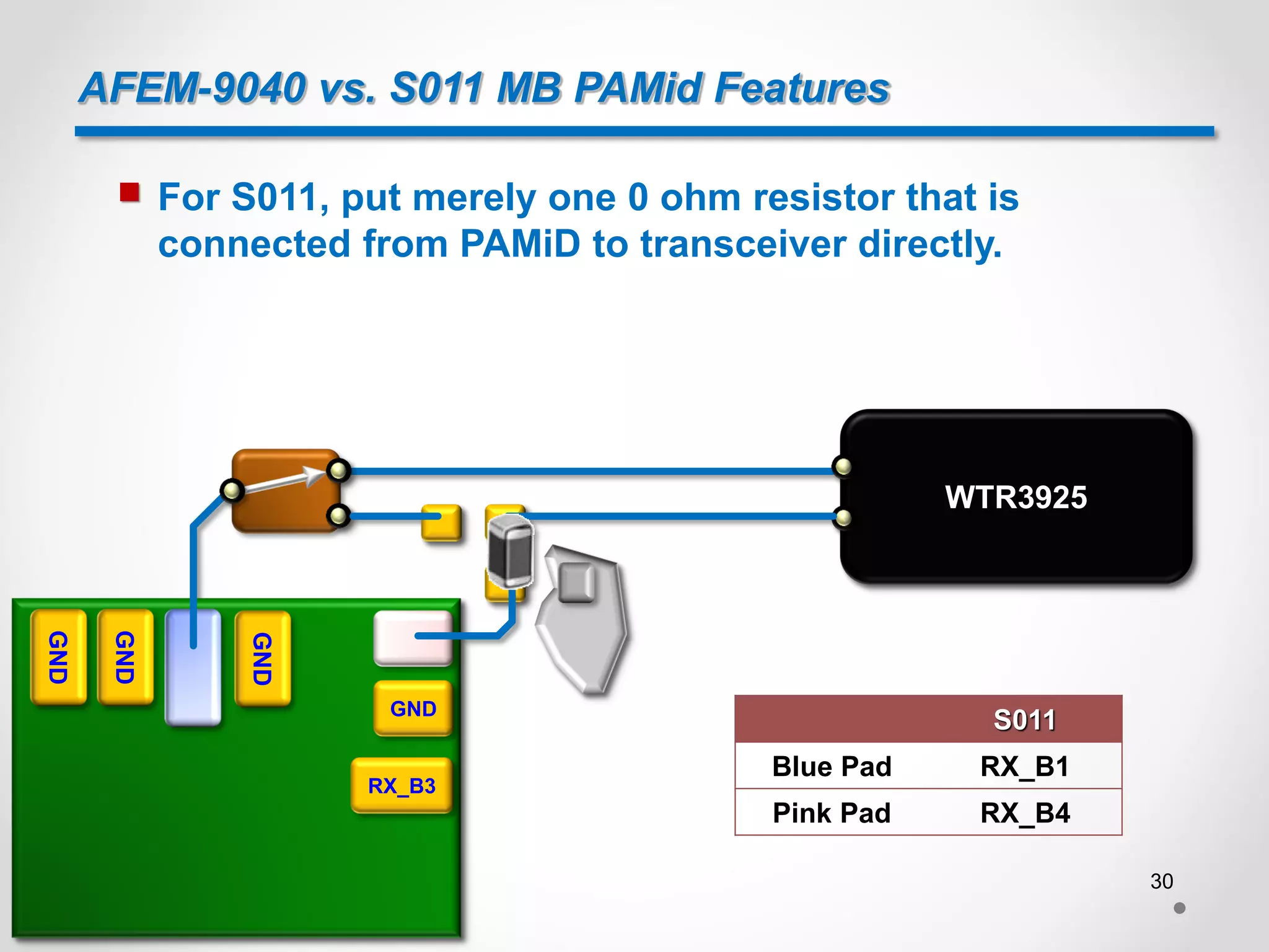
![AFEM-9040 vs. S011 MB PAMid Features
For B1 and B4 Rx, the connection between transceiver
and PAMiD for AFEM-9040 and S011 is as below[5]:
RX_B1_B4
SPDT
WTR3925
RX_B1
RX_B4 AFEM-9040
WTR3925
RX_B1
RX_B4 S011
27](https://image.slidesharecdn.com/introductiontopamid-161130141335/75/Introduction-to-PAMiD-27-2048.jpg)


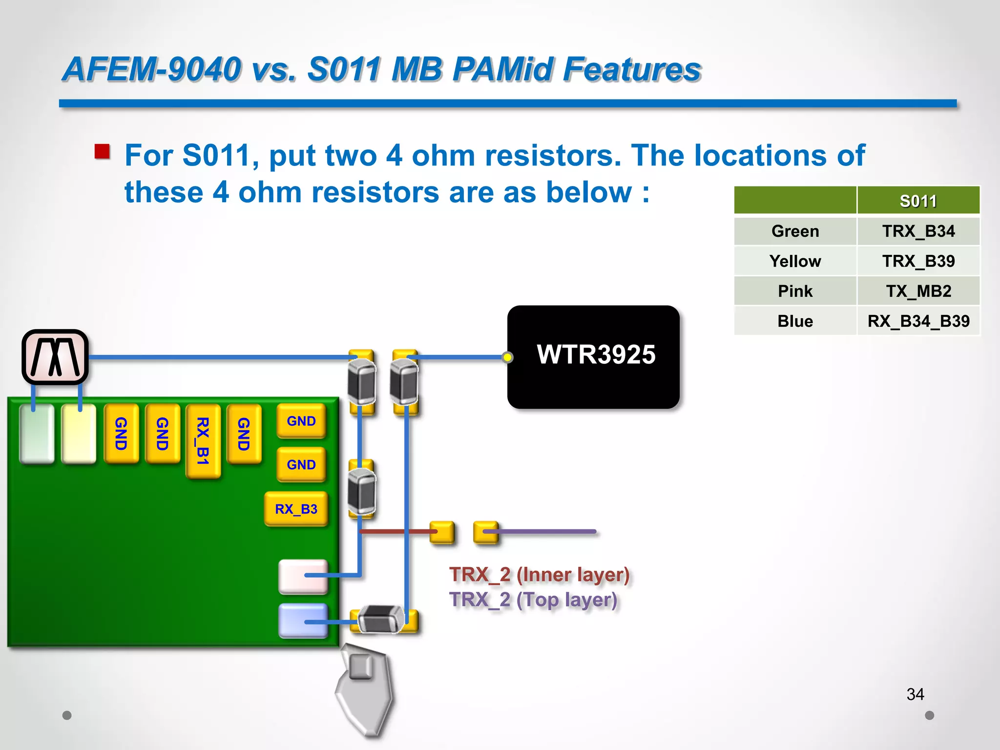
![AFEM-9040 vs. S011 MB PAMid Features
For B34 and B39, the connection between transceiver
and PAMiD for AFEM-9040 and S011 is as below[5]:
RX_B34_B39
Diplexer
AFEM-9040
RX_B39
RX_B34 WTR3925
RX_B34_B39
Diplexer
S011 WTR3925
TRX_B34_B39
TRX_B34
TRX_B39
31](https://image.slidesharecdn.com/introductiontopamid-161130141335/75/Introduction-to-PAMiD-31-2048.jpg)


![Reference
[1] Qualcomm and TDK Joint Venture, Qualcomm
[2] S011 TDK MB PAMiD Band 1, 2, 3, and 4, Device Specification, Qualcomm
[3] S011 TDK MB PAMID Design Checklist, Qualcomm
[4] Avago PAMid vs. Qcom PAMid, AVAGO
[5] WTR3925 + WTR4905 + Qualcomm RF360™ with HB, MB, and LB PAMiD Global 3DL CA
Design Example, Qualcomm
35](https://image.slidesharecdn.com/introductiontopamid-161130141335/75/Introduction-to-PAMiD-35-2048.jpg)

This document provides information about the Qualcomm S011 PAMiD module, including its applications, schematics, layout guidelines, and a comparison to the Avago AFEM-9040 PAMiD module. The S011 supports LTE, WCDMA, HSUPA bands 1-4 and carrier aggregation. Layout recommendations include separating it from other heat sources, using wide traces for power supplies, and adding vias for power and ground planes. While not pin compatible, the AFEM-9040 has a similar block diagram and footprint, requiring minor modifications for co-design.