Downloaded 381 times

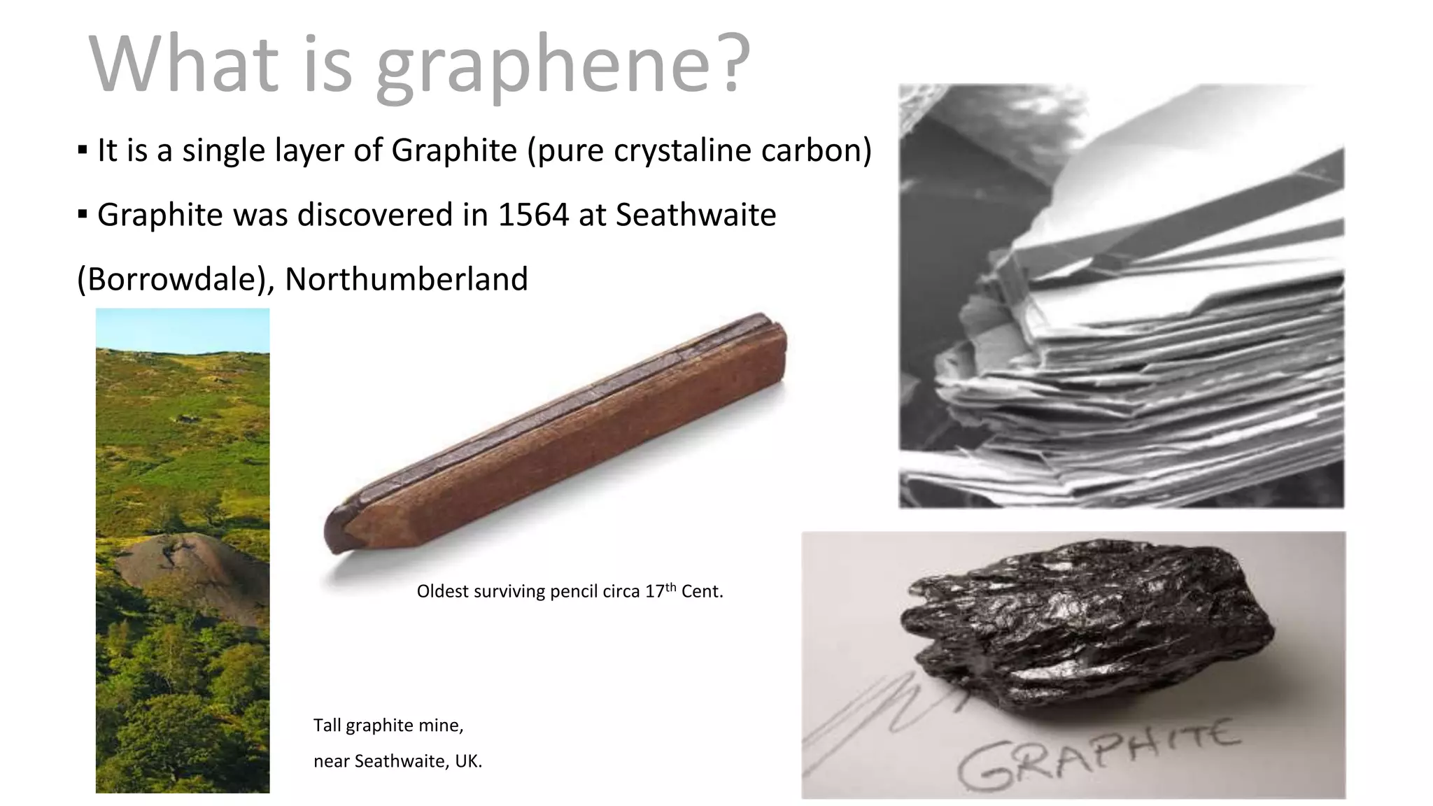

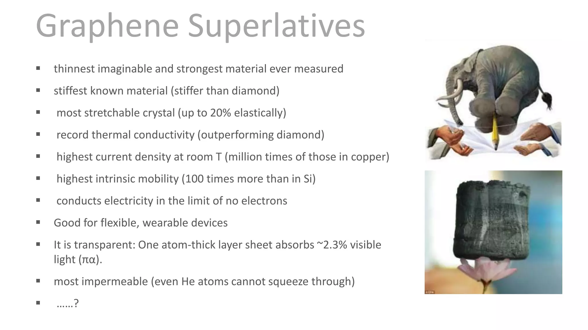
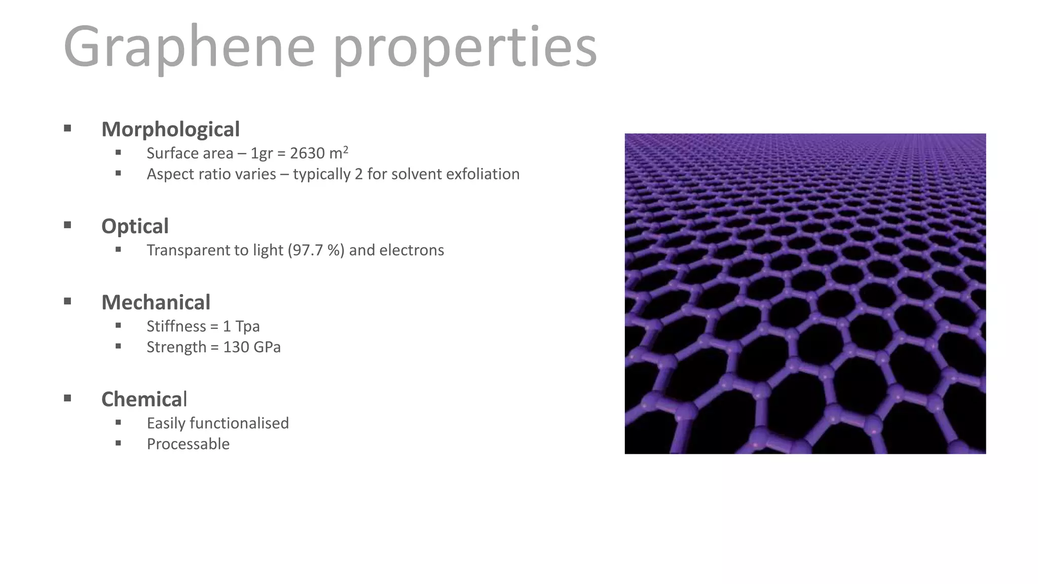
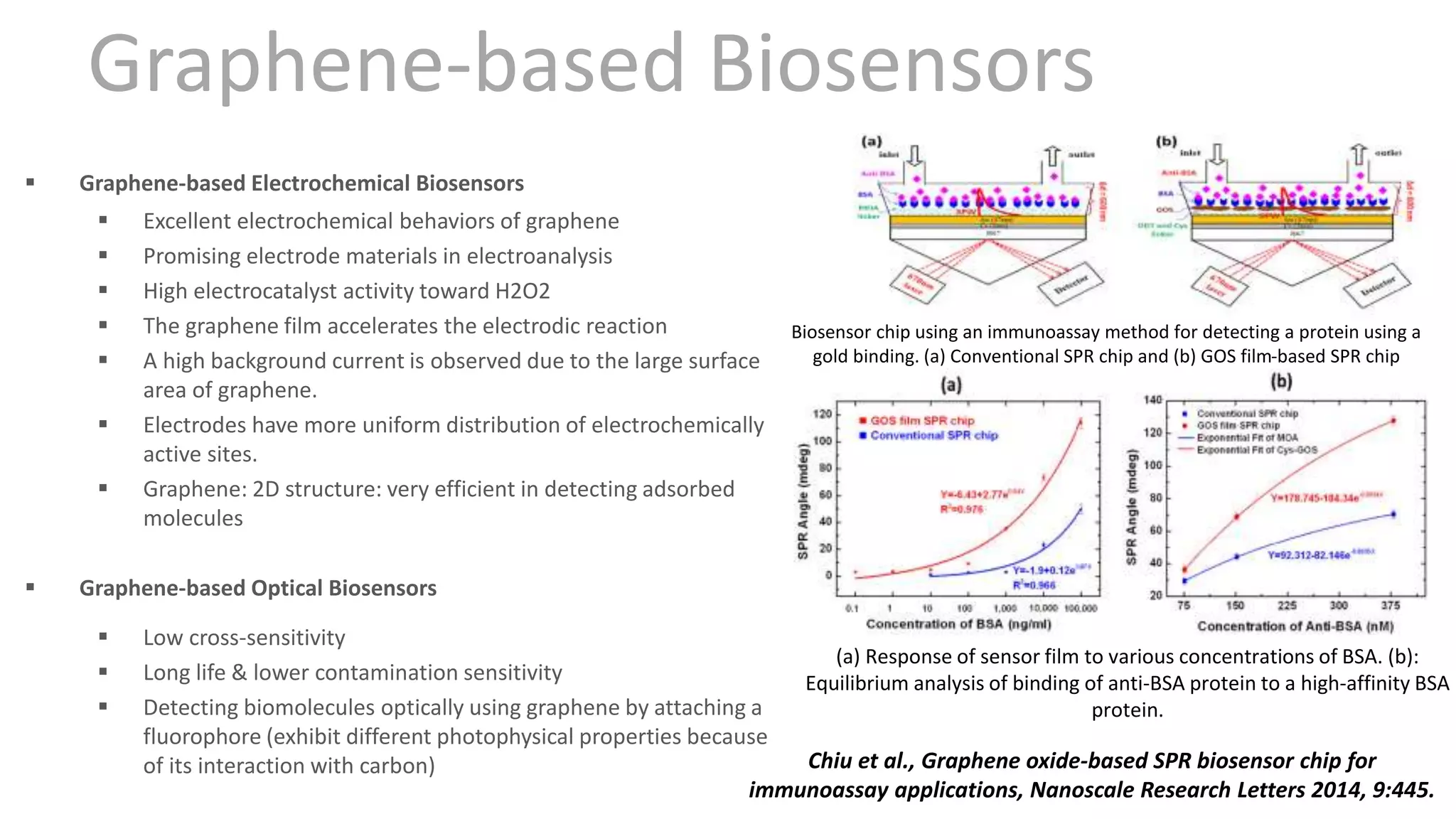
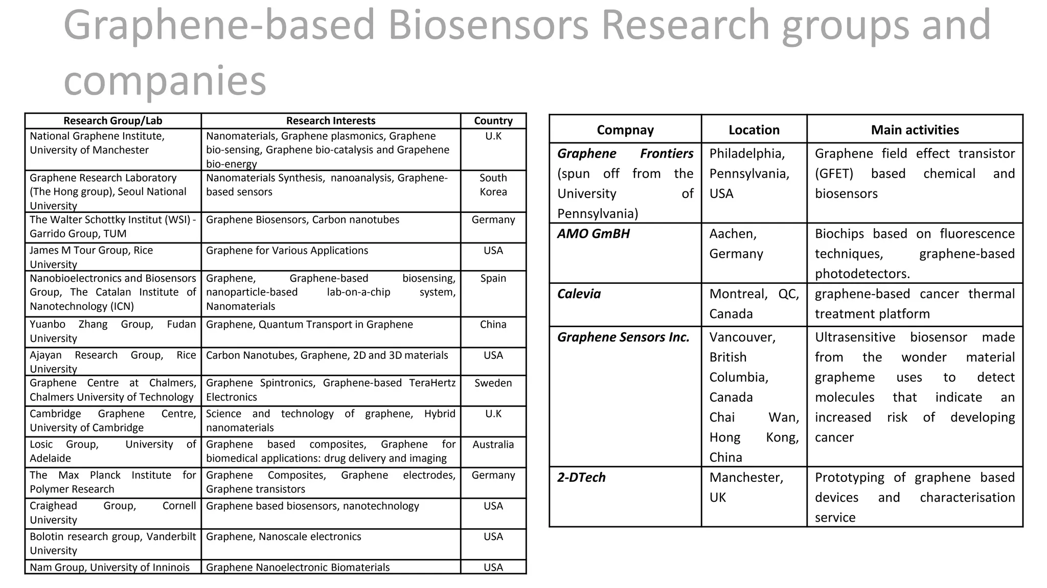
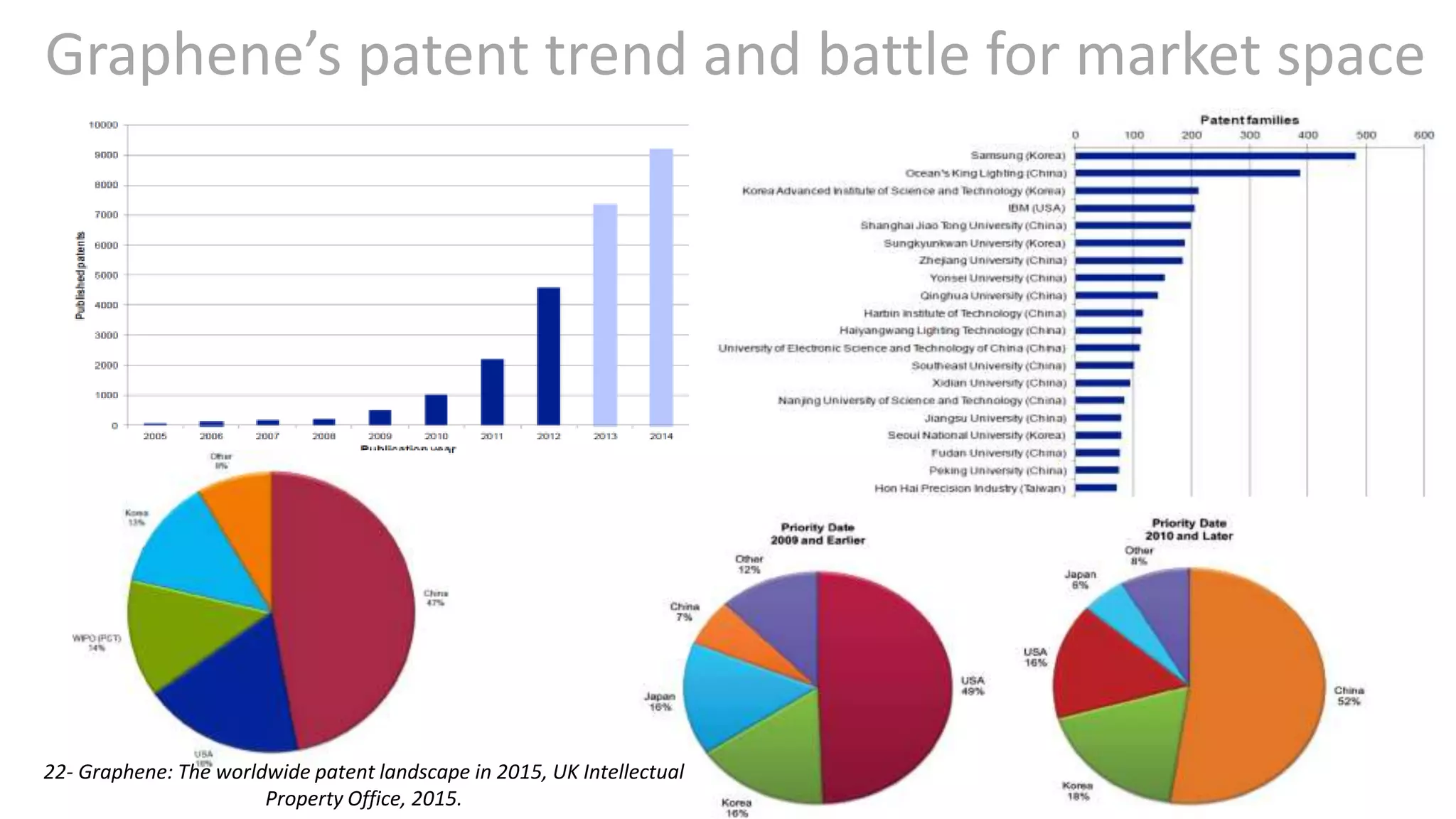


Graphene is a single layer of graphite that was first isolated in 2004. It has many superlative properties including strength, conductivity, and flexibility. These properties make it promising for applications in biosensing. Graphene-based biosensors can be electrochemical, optical, or detect DNA. They offer benefits like high sensitivity, selectivity, and a uniform electrode surface. Many research groups and companies around the world are developing graphene biosensors for applications in healthcare, electronics, and other fields. Graphene patent activity is also increasing as companies seek to commercialize the technology.


