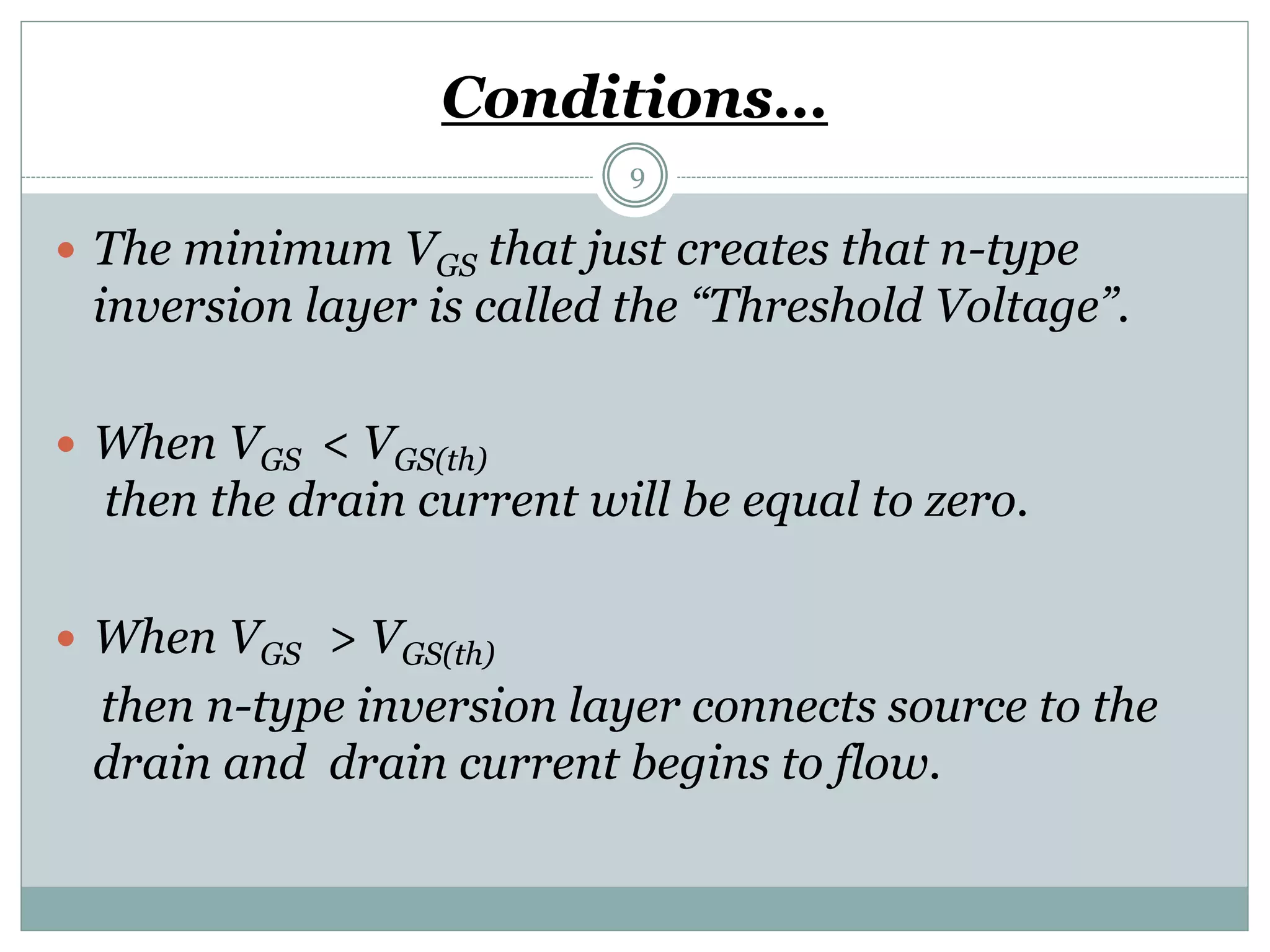
PRESENTED BY :
SHEIKH ABDUL WAHAB
WAHAB ALI
SYED BILAL HAIDER
SYED MUHAMMAD ZEEJAH HASHMI
PRESENTED TO:
MISS FARWAH AHMED
ENHANCED MOSFET
(EMOSFET)
1
MOSFET
2
 MOSFET stands for (Metal Oxide Semiconductor
Field Effect Transistor)
 It is a semiconductor device which is widely used in
switching and amplification in electronic devices.
 The MOSFET is a four terminal device having
Source (S), Gate (G), Body(B), Drain (D).
CONTD…
3
 The MOSFET works electronically by varying the
width of a channel along with charge carriers flow
(electrons or holes). The charge carriers enters
through source and exit via drain.
DEPLETION MOSFET ENHANCEMENT MOSFET
4
TYPES OF MOSFET
GRAPHICAL REPRESENTATION
5
ENHANCEMENT MODE MOSFET
6
 Enhancement-mode MOSFETs are the common
switching elements in most MOS. These devices are
off at zero gate–source voltage, and can be turned
on by pulling the gate voltage either higher than the
source voltage.
 When the gate voltage is zero then the current
between source and gate is zero, that’s why
normally E-MOSFET is normally off when gate
voltage is zero.
7
1.The drain and the
source are connected
to n-doped regions
2.These n-doped regions
are not connected to
any external source
3.The gate connected to
the p-doped
substrate through
SiO2 thin layer
4. Figure shows the
structure of N-
channel E-MOSFET.
At this stage there is
no source voltage
applied on it so there
will be no movement
of free electrons
from source to drain
and “VGS =0” here.
8
We can get the current
only through positive
gate to source (VGS)
voltage, when the gate
to source is positive it
attracts electrons into P-
region and then
recombine with the
holes. When the gate
voltage is positive
enough, so electrons
begin to flow from
source to drain.
This effect creates a thin
n-type inversion layer
through this layer free
electrons can easily flow
from source to drain.
Conditions…
9
 The minimum VGS that just creates that n-type
inversion layer is called the “Threshold Voltage”.
 When VGS < VGS(th)
then the drain current will be equal to zero.
 When VGS > VGS(th)
then n-type inversion layer connects source to the
drain and drain current begins to flow.
10
DRAIN CURVES
Figure show the drain
curves for E-MOSFET
for very low drain to
source voltage.
The lowest curve shows
when VGS < VGS(t) then
the drain current is
almost zero and the
drain current line
touches x-axis.
As soon as VGS starts
raising and at the stage
when VGS > VGS(t) then
drain current starts on
increasing as shown in
the graph.
11
TRANSCONDUCTANCE CURVE…
There is no current until
VGS =VGS (t)
The drain current
then rapidly
increases until it
reaches the
saturation current
ID (sat) beyond this
point the device is
biased in the Ohmic
region therefore ID
(sat) remains constant
, even though VGS
increases to ensure
hard saturation, a
gate voltage of VGS(on)
is uesd well above
VGS(t) as shown in
graph
12
BIASING IN OHMIC REGION
When E-MOSFET is
biased in the ohmic
region there is a Qtest
point in that region at
VGS= VGS(on) curve the
manufacturer measures
ID(on) and VDS(on) at this
Qtest point.
Manufacturer calculates
the value of RDS (on) by
using the ohm’s law,
the formula is
RDS(on) = VDS (on) / IDS (on)”
13
The figure shows the
load line between
saturation current
ID(sat) and the cut off
voltage VDD
When VGS = 0 then the
“Q” point is at the lower
end of the dc load line
and when the “Q” point
is below the Q(test)
point then the device is
biased in the ohmic
region in other word the
E-MOSFET is biased in
the ohmic region when
“ID(sat) < ID(on) and
“VGS = VGS(on)”
14
JAZAK ALLAH…. !!!

Emosfet slides....

  • 1.
    PRESENTED BY : SHEIKHABDUL WAHAB WAHAB ALI SYED BILAL HAIDER SYED MUHAMMAD ZEEJAH HASHMI PRESENTED TO: MISS FARWAH AHMED ENHANCED MOSFET (EMOSFET) 1
  • 2.
    MOSFET 2  MOSFET standsfor (Metal Oxide Semiconductor Field Effect Transistor)  It is a semiconductor device which is widely used in switching and amplification in electronic devices.  The MOSFET is a four terminal device having Source (S), Gate (G), Body(B), Drain (D).
  • 3.
    CONTD… 3  The MOSFETworks electronically by varying the width of a channel along with charge carriers flow (electrons or holes). The charge carriers enters through source and exit via drain.
  • 4.
    DEPLETION MOSFET ENHANCEMENTMOSFET 4 TYPES OF MOSFET
  • 5.
  • 6.
    ENHANCEMENT MODE MOSFET 6 Enhancement-mode MOSFETs are the common switching elements in most MOS. These devices are off at zero gate–source voltage, and can be turned on by pulling the gate voltage either higher than the source voltage.  When the gate voltage is zero then the current between source and gate is zero, that’s why normally E-MOSFET is normally off when gate voltage is zero.
  • 7.
    7 1.The drain andthe source are connected to n-doped regions 2.These n-doped regions are not connected to any external source 3.The gate connected to the p-doped substrate through SiO2 thin layer 4. Figure shows the structure of N- channel E-MOSFET. At this stage there is no source voltage applied on it so there will be no movement of free electrons from source to drain and “VGS =0” here.
  • 8.
    8 We can getthe current only through positive gate to source (VGS) voltage, when the gate to source is positive it attracts electrons into P- region and then recombine with the holes. When the gate voltage is positive enough, so electrons begin to flow from source to drain. This effect creates a thin n-type inversion layer through this layer free electrons can easily flow from source to drain.
  • 9.
    Conditions… 9  The minimumVGS that just creates that n-type inversion layer is called the “Threshold Voltage”.  When VGS < VGS(th) then the drain current will be equal to zero.  When VGS > VGS(th) then n-type inversion layer connects source to the drain and drain current begins to flow.
  • 10.
    10 DRAIN CURVES Figure showthe drain curves for E-MOSFET for very low drain to source voltage. The lowest curve shows when VGS < VGS(t) then the drain current is almost zero and the drain current line touches x-axis. As soon as VGS starts raising and at the stage when VGS > VGS(t) then drain current starts on increasing as shown in the graph.
  • 11.
    11 TRANSCONDUCTANCE CURVE… There isno current until VGS =VGS (t) The drain current then rapidly increases until it reaches the saturation current ID (sat) beyond this point the device is biased in the Ohmic region therefore ID (sat) remains constant , even though VGS increases to ensure hard saturation, a gate voltage of VGS(on) is uesd well above VGS(t) as shown in graph
  • 12.
    12 BIASING IN OHMICREGION When E-MOSFET is biased in the ohmic region there is a Qtest point in that region at VGS= VGS(on) curve the manufacturer measures ID(on) and VDS(on) at this Qtest point. Manufacturer calculates the value of RDS (on) by using the ohm’s law, the formula is RDS(on) = VDS (on) / IDS (on)”
  • 13.
    13 The figure showsthe load line between saturation current ID(sat) and the cut off voltage VDD When VGS = 0 then the “Q” point is at the lower end of the dc load line and when the “Q” point is below the Q(test) point then the device is biased in the ohmic region in other word the E-MOSFET is biased in the ohmic region when “ID(sat) < ID(on) and “VGS = VGS(on)”
  • 14.