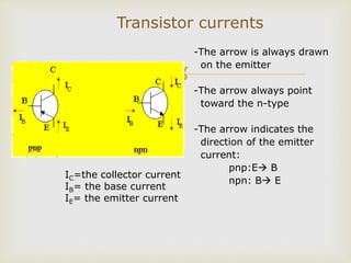
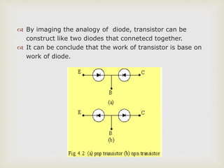
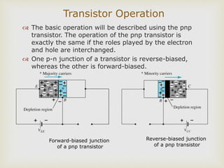
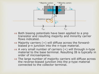
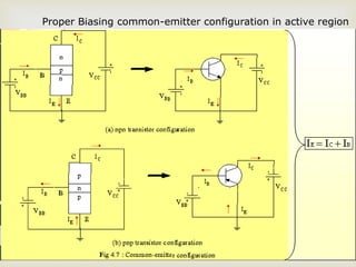
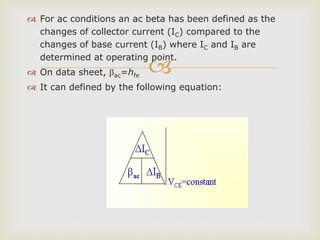
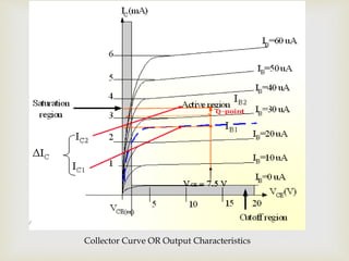
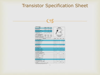
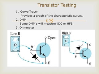
SHANTILAL SHAH GOVERNMENT
ENGINEERING COLLEGE, BHAVNAGAR
Postal Address : New Sidsar Campus
Post : Vartej, Sidsar, Bhavnagar-364060, Gujarat, India
Contact : 0278-2445509,2445767 Fax : 0278-2445509
Website: http://www.ssgec.ac.in/
Roll No. Enrollment No. Name
3017 140430117019 JITIN J PILLAI
3010 140430117012 PARTH DODIYA
3016 140430117018 ISHAN J BHATT
Department : INSTRUMENTATION & CONTROL
Course : B.E. (2014 Batch)
Semester : 3rd
Batch : B1
PREPARED BY :
BIPOLAR JUNCTION
TRANSISTOR
Subject:
ELECTRONIC DEVICES &
CIRCUITS (2131006)
 The basic of electronic system nowadays is
semiconductor device.
 The famous and commonly use of this device
is BJTs
(Bipolar Junction Transistors).
 It can be use as amplifier and logic switches.
 BJT consists of three terminal:
 collector : C
 base : B
emitter : E
 Two types of BJT : pnp and npn
Introduction
Transistor Construction
 3 layer semiconductor device consisting:
 2 n- and 1 p-type layers of material  npn transistor
 2 p- and 1 n-type layers of material pnp transistor
 The term bipolar reflects the fact that holes and
electrons participate in the injection process into the
oppositely polarized material
 A single pn junction has two different types of bias:
 forward bias
 reverse bias
 Thus, a two-pn-junction device has four types of bias.

Position of the terminals and symbol of
BJT.
• Base is located at the middle
and more thin from the level
of collector and emitter
• The emitter and collector
terminals are made of the
same type of semiconductor
material, while the base of the
other type of material

Transistor currents
-The arrow is always drawn
on the emitter
-The arrow always point
toward the n-type
-The arrow indicates the
direction of the emitter
current:
pnp:E B
npn: B E
IC=the collector current
IB= the base current
IE= the emitter current
 By imaging the analogy of diode, transistor can be
construct like two diodes that connetecd together.
 It can be conclude that the work of transistor is base on
work of diode.
Transistor Operation
 The basic operation will be described using the pnp
transistor. The operation of the pnp transistor is
exactly the same if the roles played by the electron
and hole are interchanged.
 One p-n junction of a transistor is reverse-biased,
whereas the other is forward-biased.
Forward-biased junction
of a pnp transistor
Reverse-biased junction
of a pnp transistor

 Both biasing potentials have been applied to a pnp
transistor and resulting majority and minority carrier
flows indicated.
 Majority carriers (+) will diffuse across the forward-
biased p-n junction into the n-type material.
 A very small number of carriers (+) will through n-type
material to the base terminal. Resulting IB is typically in
order of microamperes.
 The large number of majority carriers will diffuse across
the reverse-biased junction into the p-type material
connected to the collector terminal.

 Majority carriers can cross the reverse-biased
junction because the injected majority carriers will
appear as minority carriers in the n-type material.
 Applying KCL to the transistor :
IE = IC + IB
 The comprises of two components – the majority
and minority carriers
IC = ICmajority + ICOminority
 ICO – IC current with emitter terminal open and is
called leakage current.

 Proper biasing CB configuration in active region by
approximation IC  IE (IB  0 uA)
Biasing

Transistor as an amplifier
 It is called common-emitter configuration since :
- emitter is common or reference to both input and
output terminals.
- emitter is usually the terminal closest to or at
ground
potential.
 Almost amplifier design is using connection of CE due
to the high gain for current and voltage.
 Two set of characteristics are necessary to describe
the behavior for CE ;input (base terminal) and output
(collector terminal) parameters.
Common-Emitter Configuration
Proper Biasing common-emitter configuration in active region

Input characteristics for a
common-emitter NPN transistor
 IB is microamperes compared
to miliamperes of IC.
 IB will flow when VBE > 0.7V
for silicon and 0.3V for
germanium
 Before this value IB is very
small and no IB.
 Base-emitter junction is
forward bias
 Increasing VCE will reduce IB
for different values.

Output characteristics for a
common-emitter npn
transistor
 For small VCE (VCE < VCESAT, IC increase linearly with
increasing of VCE
 VCE > VCESAT IC not totally depends on VCE  constant IC
 IB(uA) is very small compare to IC (mA). Small increase in
IB cause big increase in IC
 IB=0 A  ICEO occur.
 Noticing the value when IC=0A. There is still some value of
current flows.

 The ratio of dc collector current (IC) to the dc base
current (IB) is dc beta (dc ) which is dc current gain
where IC and IB are determined at a particular operating
point, Q-point (quiescent point).
 It’s define by the following equation:
30 < dc < 300  2N3904
 On data sheet, dc=hFE with h is derived from ac hybrid
equivalent cct. FE are derived from forward-current
amplification and common-emitter configuration
respectively.
Beta () or amplification factor

 For ac conditions an ac beta has been defined as the
changes of collector current (IC) compared to the
changes of base current (IB) where IC and IB are
determined at operating point.
 On data sheet, ac=hfe
 It can defined by the following equation:
Collector Curve OR Output Characteristics

Transistor Specification Sheet

Transistor Terminal Identification

1. Curve Tracer
Provides a graph of the characteristic curves.
2. DMM
Some DMM’s will measure DC or HFE.
3. Ohmmeter
Transistor Testing
EDC_2131006_BipolarJunctionTransistor

EDC_2131006_BipolarJunctionTransistor

  • 1.
    SHANTILAL SHAH GOVERNMENT ENGINEERINGCOLLEGE, BHAVNAGAR Postal Address : New Sidsar Campus Post : Vartej, Sidsar, Bhavnagar-364060, Gujarat, India Contact : 0278-2445509,2445767 Fax : 0278-2445509 Website: http://www.ssgec.ac.in/ Roll No. Enrollment No. Name 3017 140430117019 JITIN J PILLAI 3010 140430117012 PARTH DODIYA 3016 140430117018 ISHAN J BHATT Department : INSTRUMENTATION & CONTROL Course : B.E. (2014 Batch) Semester : 3rd Batch : B1 PREPARED BY :
  • 2.
  • 3.
     The basicof electronic system nowadays is semiconductor device.  The famous and commonly use of this device is BJTs (Bipolar Junction Transistors).  It can be use as amplifier and logic switches.  BJT consists of three terminal:  collector : C  base : B emitter : E  Two types of BJT : pnp and npn Introduction
  • 4.
    Transistor Construction  3layer semiconductor device consisting:  2 n- and 1 p-type layers of material  npn transistor  2 p- and 1 n-type layers of material pnp transistor  The term bipolar reflects the fact that holes and electrons participate in the injection process into the oppositely polarized material  A single pn junction has two different types of bias:  forward bias  reverse bias  Thus, a two-pn-junction device has four types of bias.
  • 5.
     Position of theterminals and symbol of BJT. • Base is located at the middle and more thin from the level of collector and emitter • The emitter and collector terminals are made of the same type of semiconductor material, while the base of the other type of material
  • 6.
     Transistor currents -The arrowis always drawn on the emitter -The arrow always point toward the n-type -The arrow indicates the direction of the emitter current: pnp:E B npn: B E IC=the collector current IB= the base current IE= the emitter current
  • 7.
     By imagingthe analogy of diode, transistor can be construct like two diodes that connetecd together.  It can be conclude that the work of transistor is base on work of diode.
  • 8.
    Transistor Operation  Thebasic operation will be described using the pnp transistor. The operation of the pnp transistor is exactly the same if the roles played by the electron and hole are interchanged.  One p-n junction of a transistor is reverse-biased, whereas the other is forward-biased. Forward-biased junction of a pnp transistor Reverse-biased junction of a pnp transistor
  • 9.
      Both biasingpotentials have been applied to a pnp transistor and resulting majority and minority carrier flows indicated.  Majority carriers (+) will diffuse across the forward- biased p-n junction into the n-type material.  A very small number of carriers (+) will through n-type material to the base terminal. Resulting IB is typically in order of microamperes.  The large number of majority carriers will diffuse across the reverse-biased junction into the p-type material connected to the collector terminal.
  • 10.
      Majority carrierscan cross the reverse-biased junction because the injected majority carriers will appear as minority carriers in the n-type material.  Applying KCL to the transistor : IE = IC + IB  The comprises of two components – the majority and minority carriers IC = ICmajority + ICOminority  ICO – IC current with emitter terminal open and is called leakage current.
  • 11.
      Proper biasingCB configuration in active region by approximation IC  IE (IB  0 uA) Biasing
  • 12.
  • 13.
     It iscalled common-emitter configuration since : - emitter is common or reference to both input and output terminals. - emitter is usually the terminal closest to or at ground potential.  Almost amplifier design is using connection of CE due to the high gain for current and voltage.  Two set of characteristics are necessary to describe the behavior for CE ;input (base terminal) and output (collector terminal) parameters. Common-Emitter Configuration
  • 14.
    Proper Biasing common-emitterconfiguration in active region
  • 15.
     Input characteristics fora common-emitter NPN transistor  IB is microamperes compared to miliamperes of IC.  IB will flow when VBE > 0.7V for silicon and 0.3V for germanium  Before this value IB is very small and no IB.  Base-emitter junction is forward bias  Increasing VCE will reduce IB for different values.
  • 16.
     Output characteristics fora common-emitter npn transistor  For small VCE (VCE < VCESAT, IC increase linearly with increasing of VCE  VCE > VCESAT IC not totally depends on VCE  constant IC  IB(uA) is very small compare to IC (mA). Small increase in IB cause big increase in IC  IB=0 A  ICEO occur.  Noticing the value when IC=0A. There is still some value of current flows.
  • 18.
      The ratioof dc collector current (IC) to the dc base current (IB) is dc beta (dc ) which is dc current gain where IC and IB are determined at a particular operating point, Q-point (quiescent point).  It’s define by the following equation: 30 < dc < 300  2N3904  On data sheet, dc=hFE with h is derived from ac hybrid equivalent cct. FE are derived from forward-current amplification and common-emitter configuration respectively. Beta () or amplification factor
  • 19.
      For acconditions an ac beta has been defined as the changes of collector current (IC) compared to the changes of base current (IB) where IC and IB are determined at operating point.  On data sheet, ac=hfe  It can defined by the following equation:
  • 20.
    Collector Curve OROutput Characteristics
  • 21.
  • 22.
  • 23.
     1. Curve Tracer Providesa graph of the characteristic curves. 2. DMM Some DMM’s will measure DC or HFE. 3. Ohmmeter Transistor Testing