Download to read offline


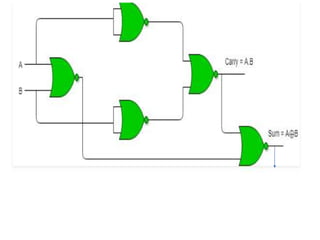
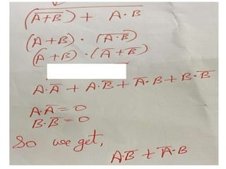
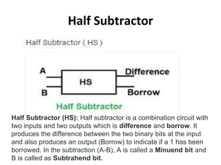
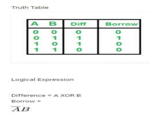
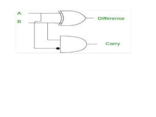
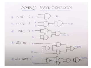
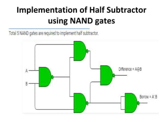
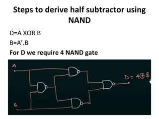
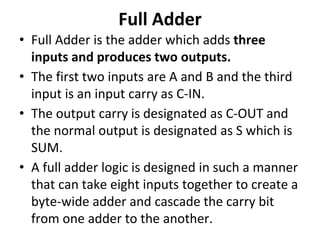
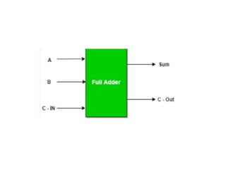
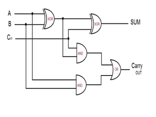
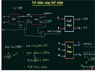
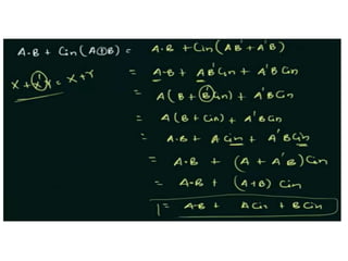
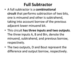
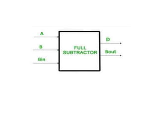
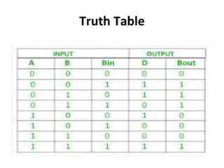
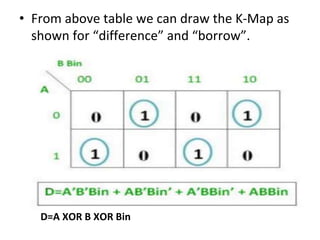
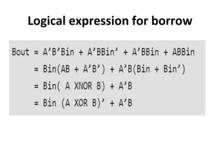
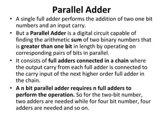
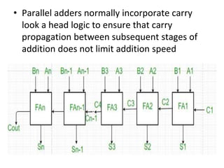
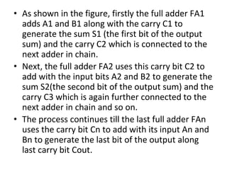
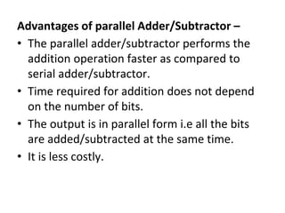
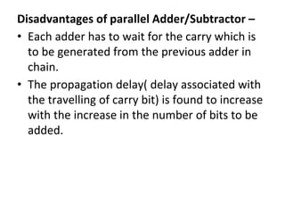
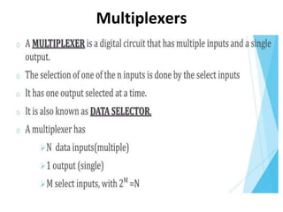
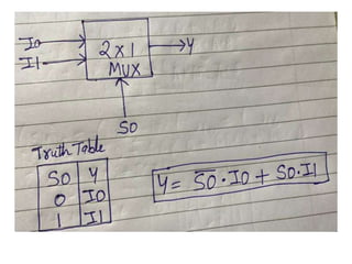
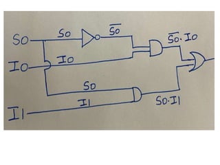
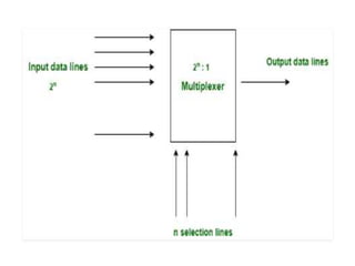
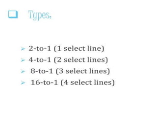
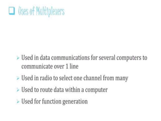
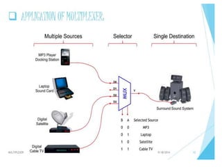
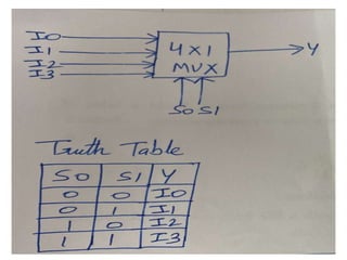
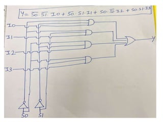
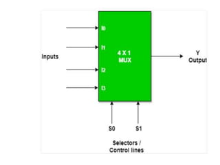
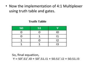
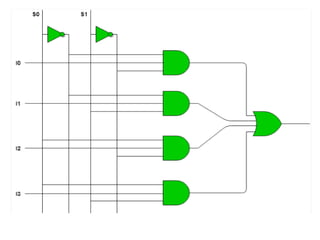
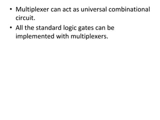
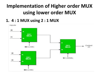
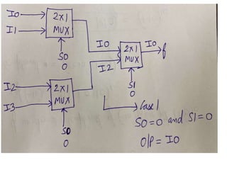
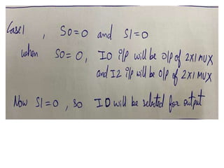
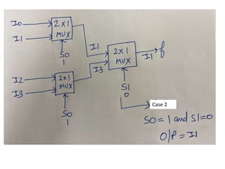
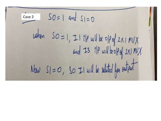
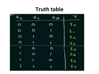
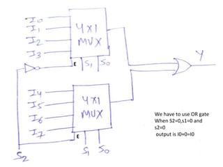
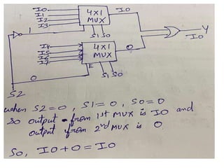
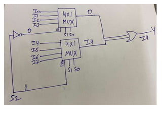
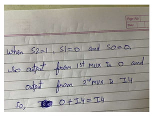
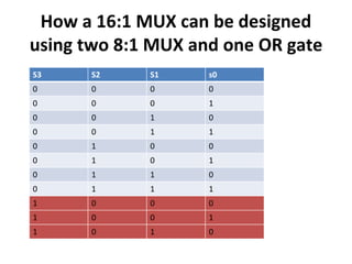
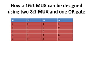
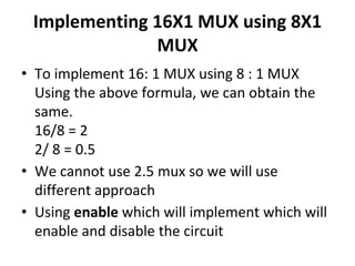
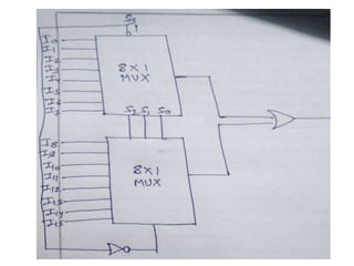
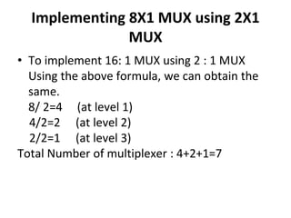
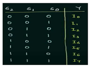
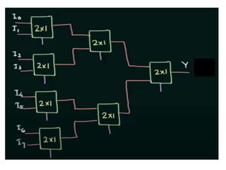
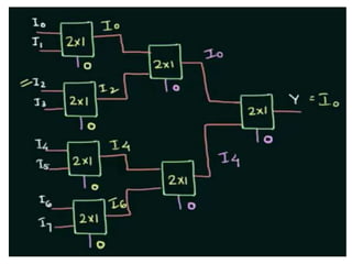
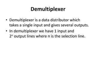
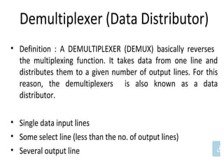
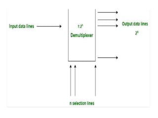
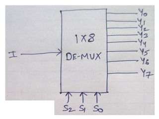
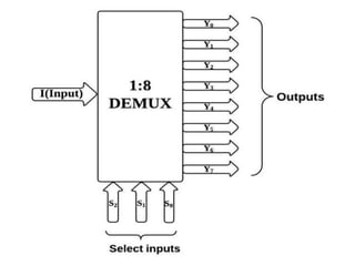
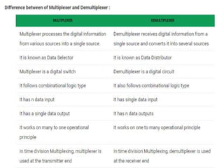
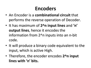
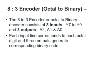
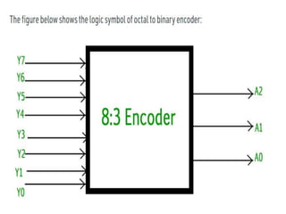
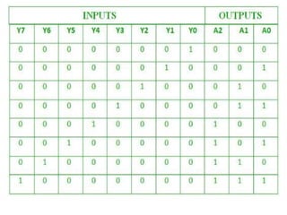
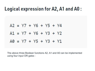
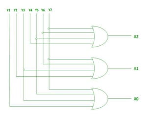
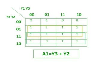
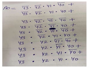
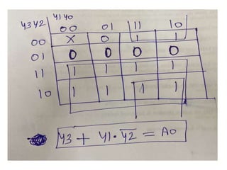
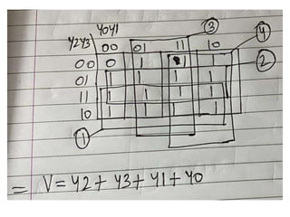
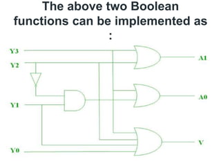
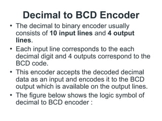
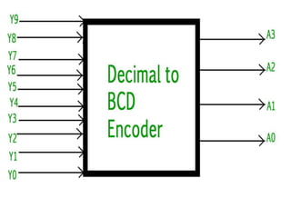
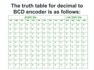
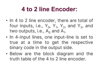
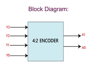
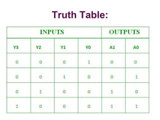
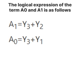
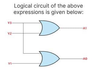
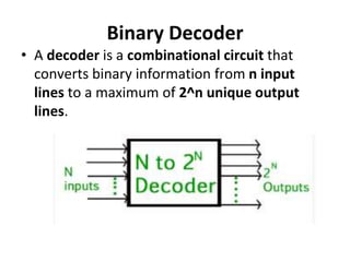
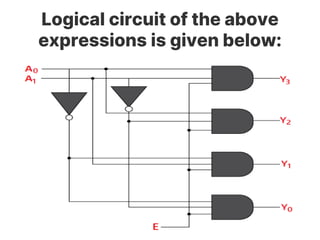
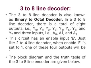
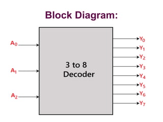
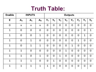
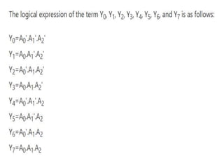
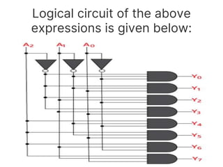
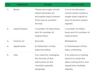
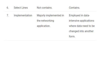
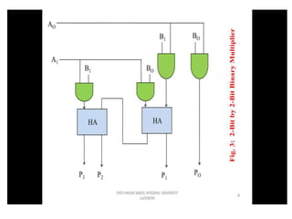
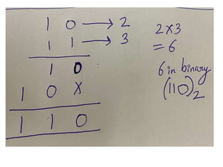
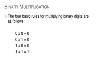
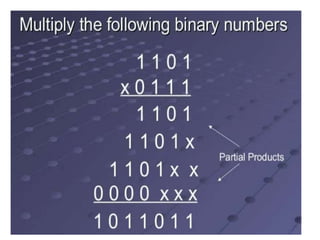
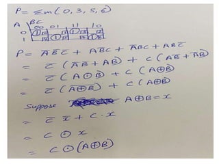
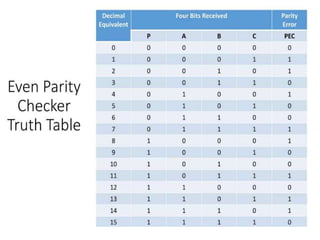
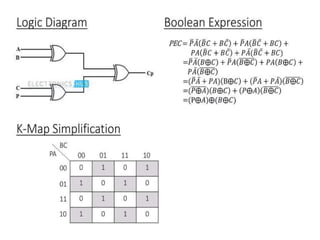

The document discusses various digital logic circuits including half adders, full adders, parallel adders, subtractors, multiplexers, demultiplexers, encoders, and decoders. It explains the basic concepts and provides examples of implementing 1-bit, 2-bit, 4-bit, and 8-bit versions of these circuits using logic gates like AND, OR, and NOT. Implementation of higher order multiplexers and decoders using lower order building blocks is also covered.