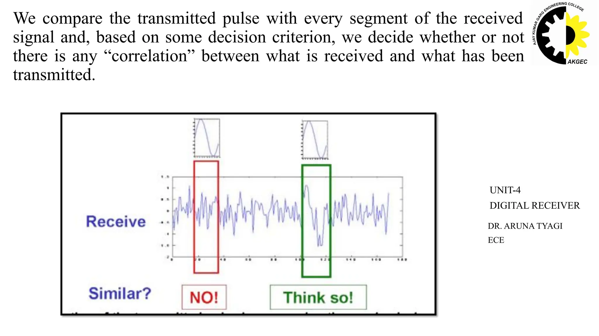
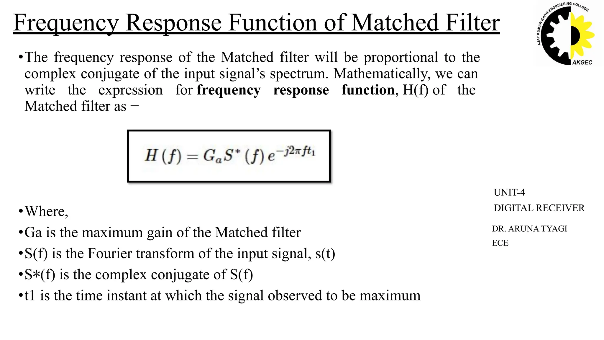
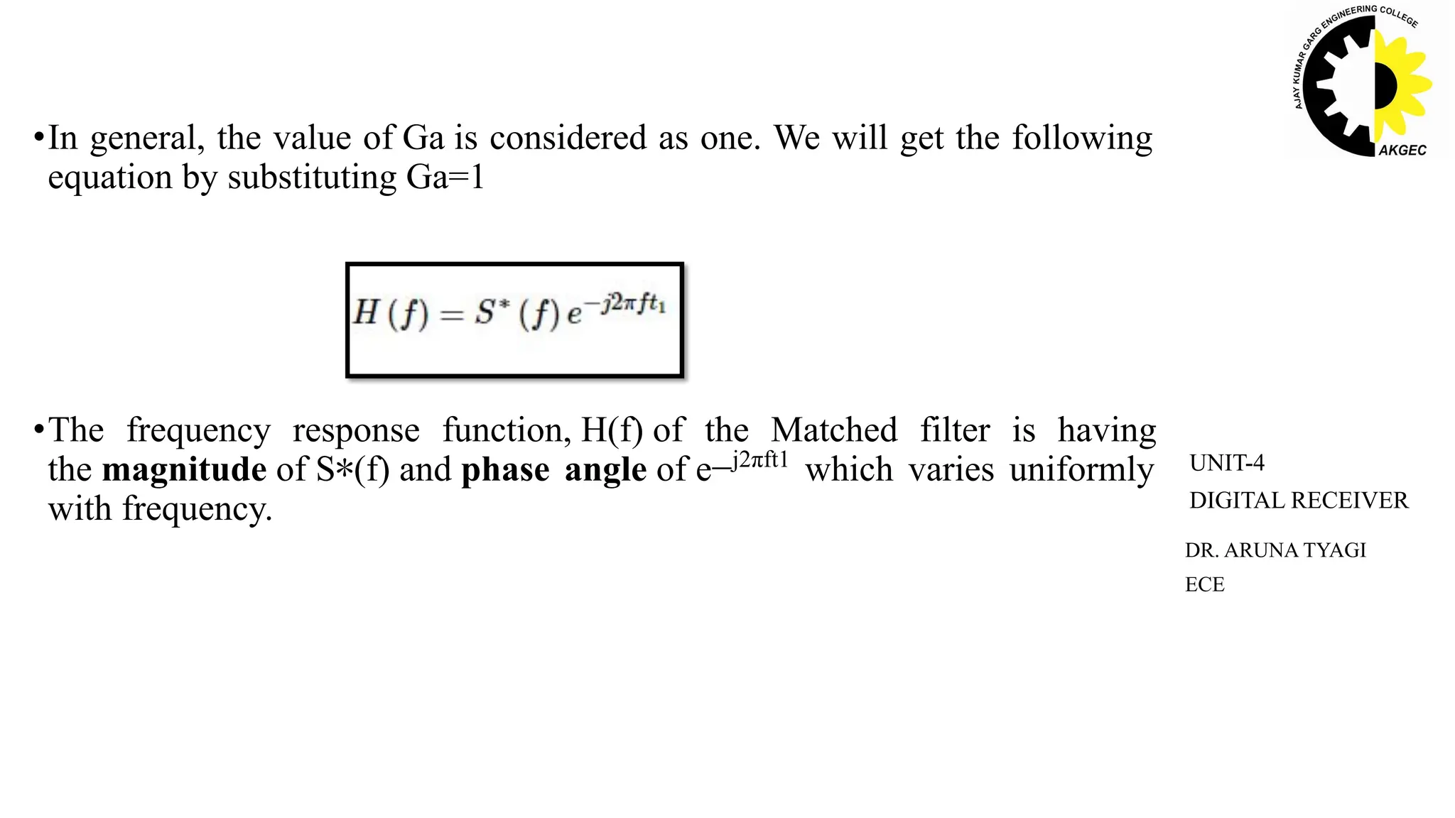
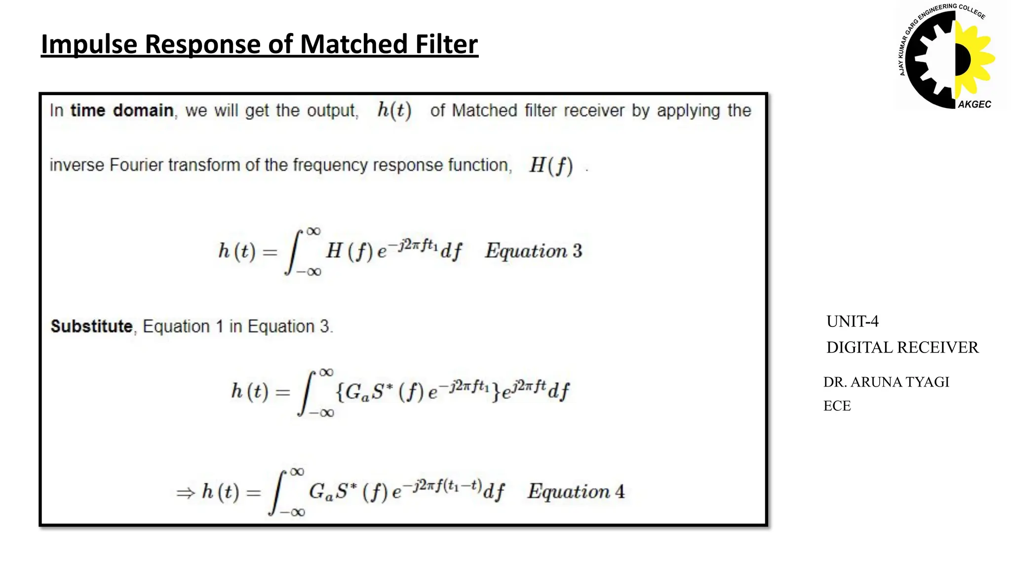
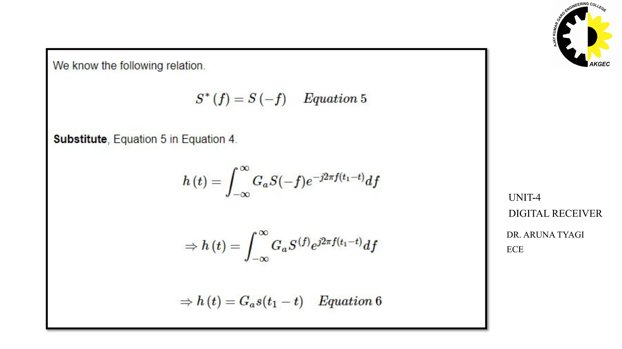
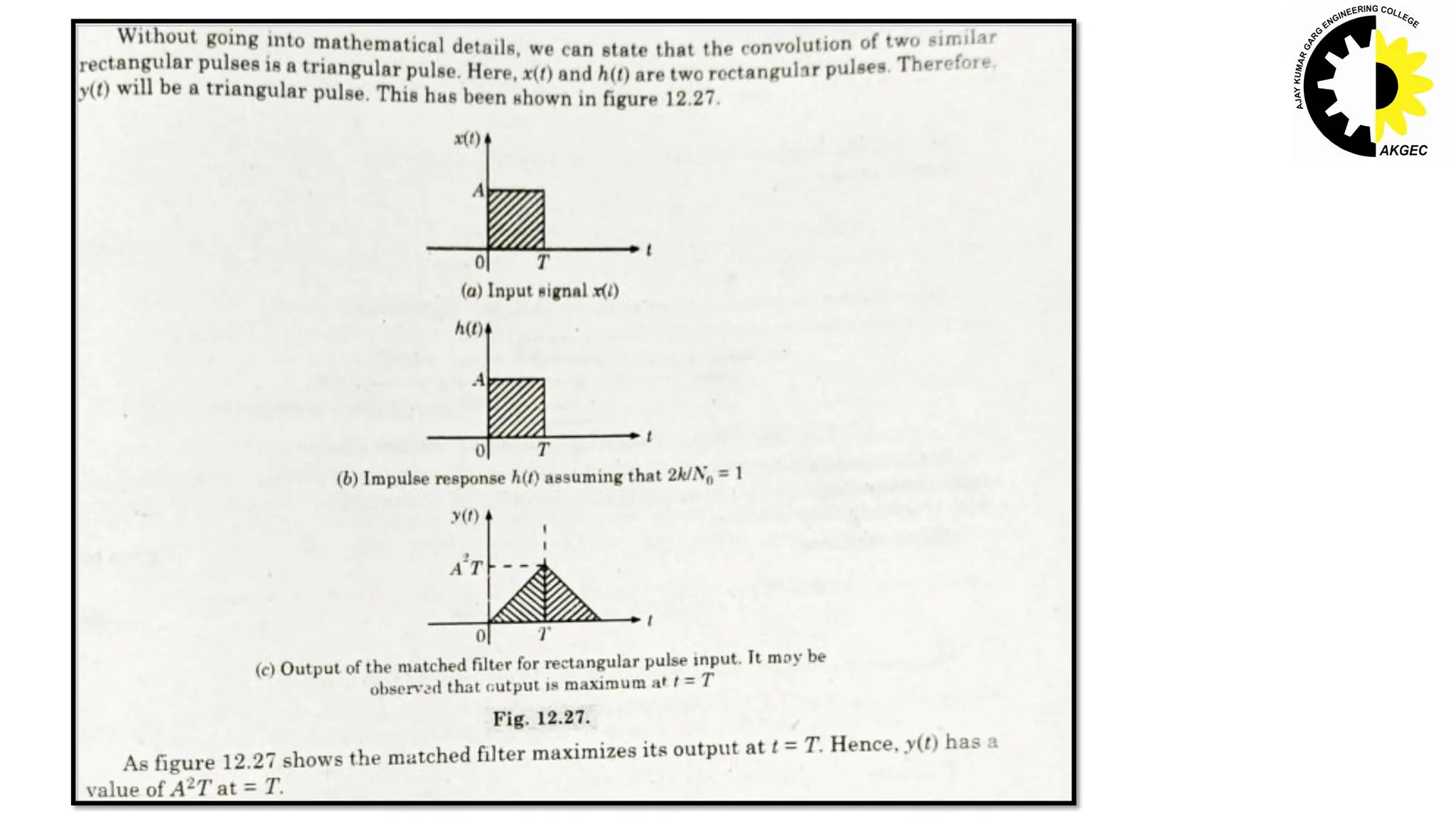
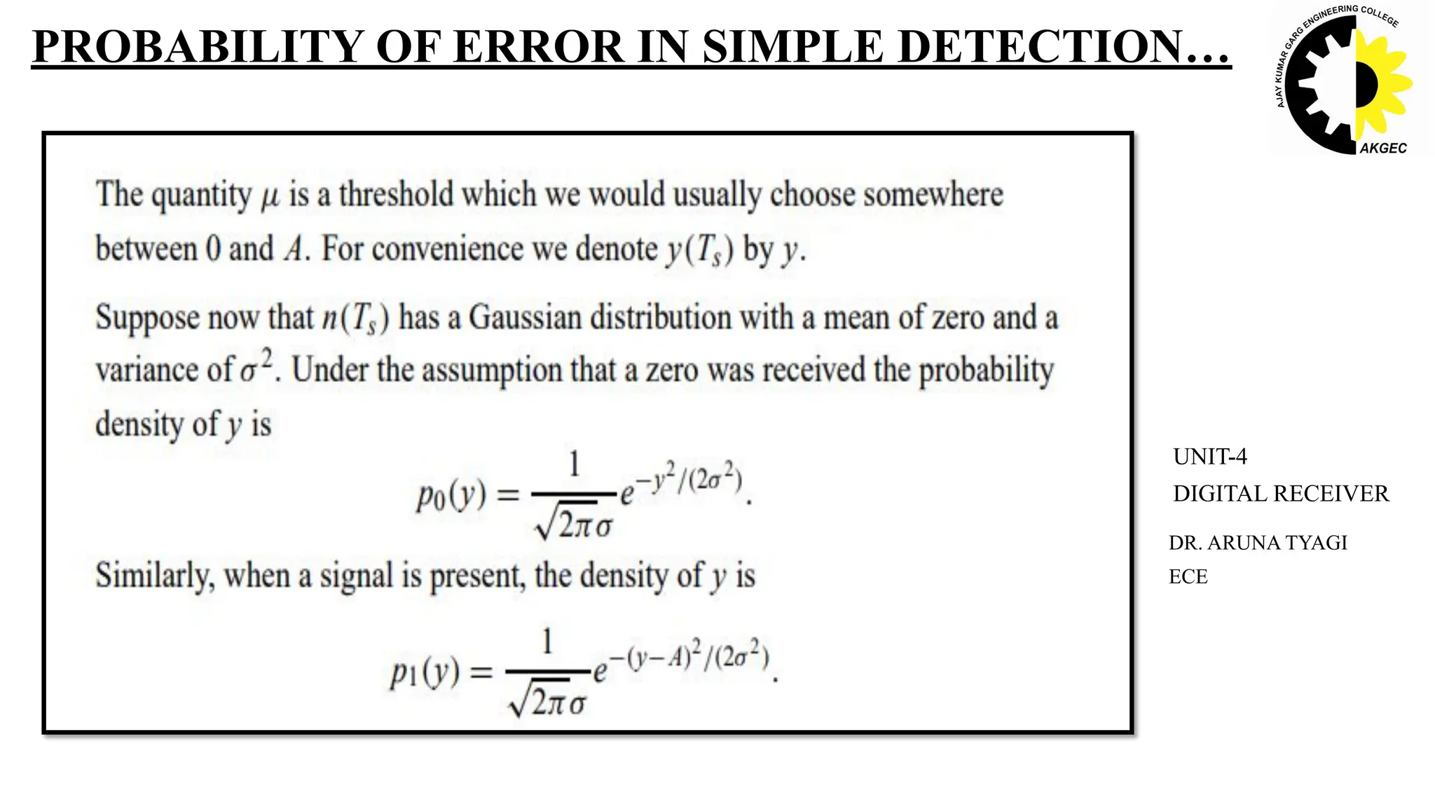
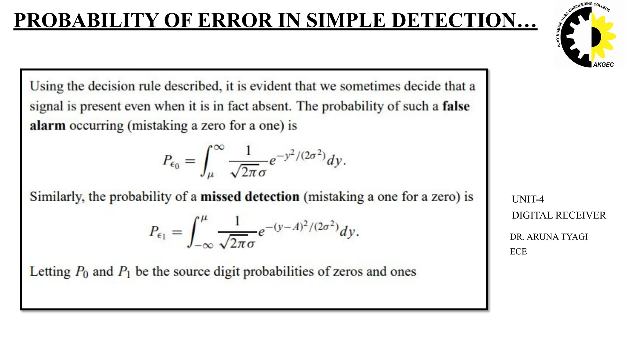
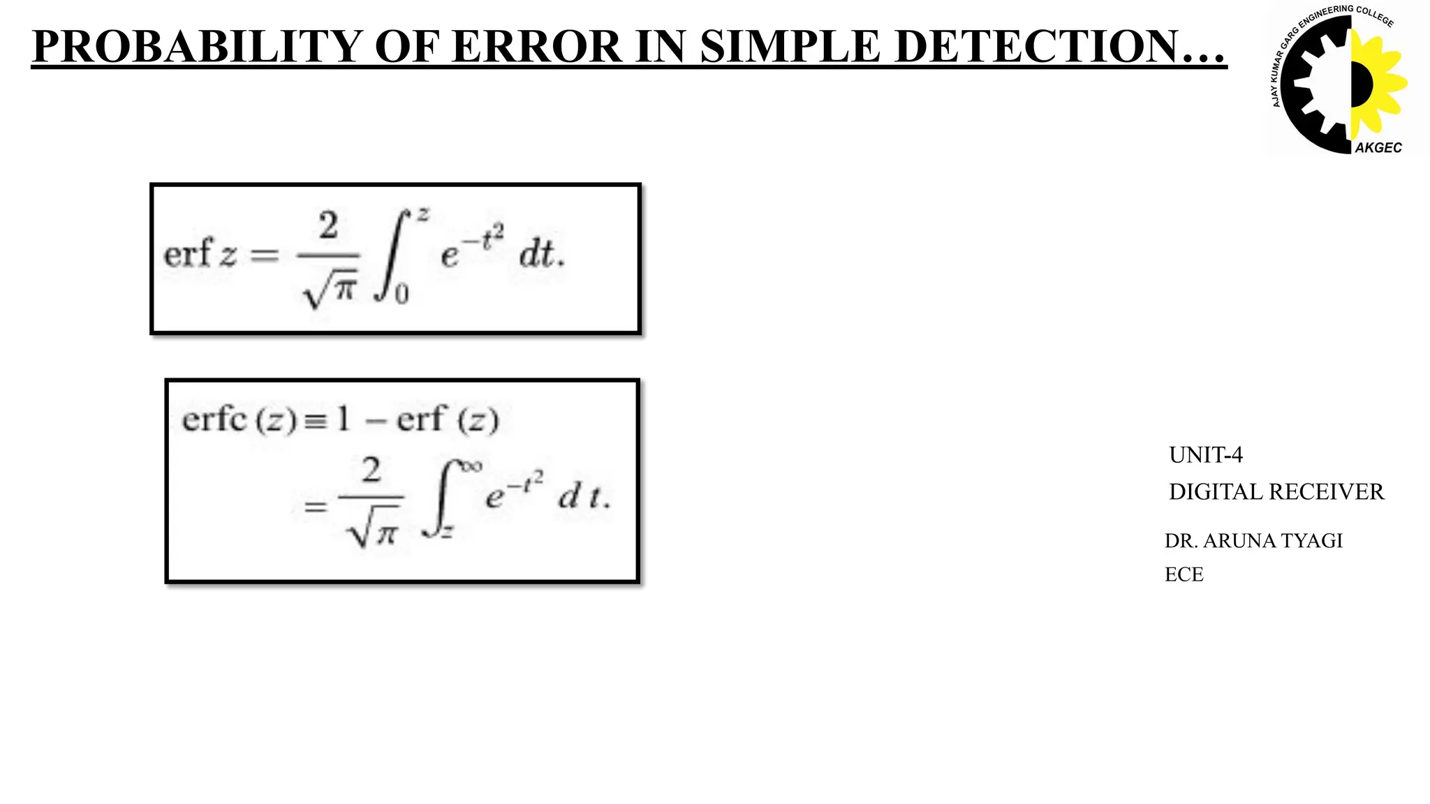
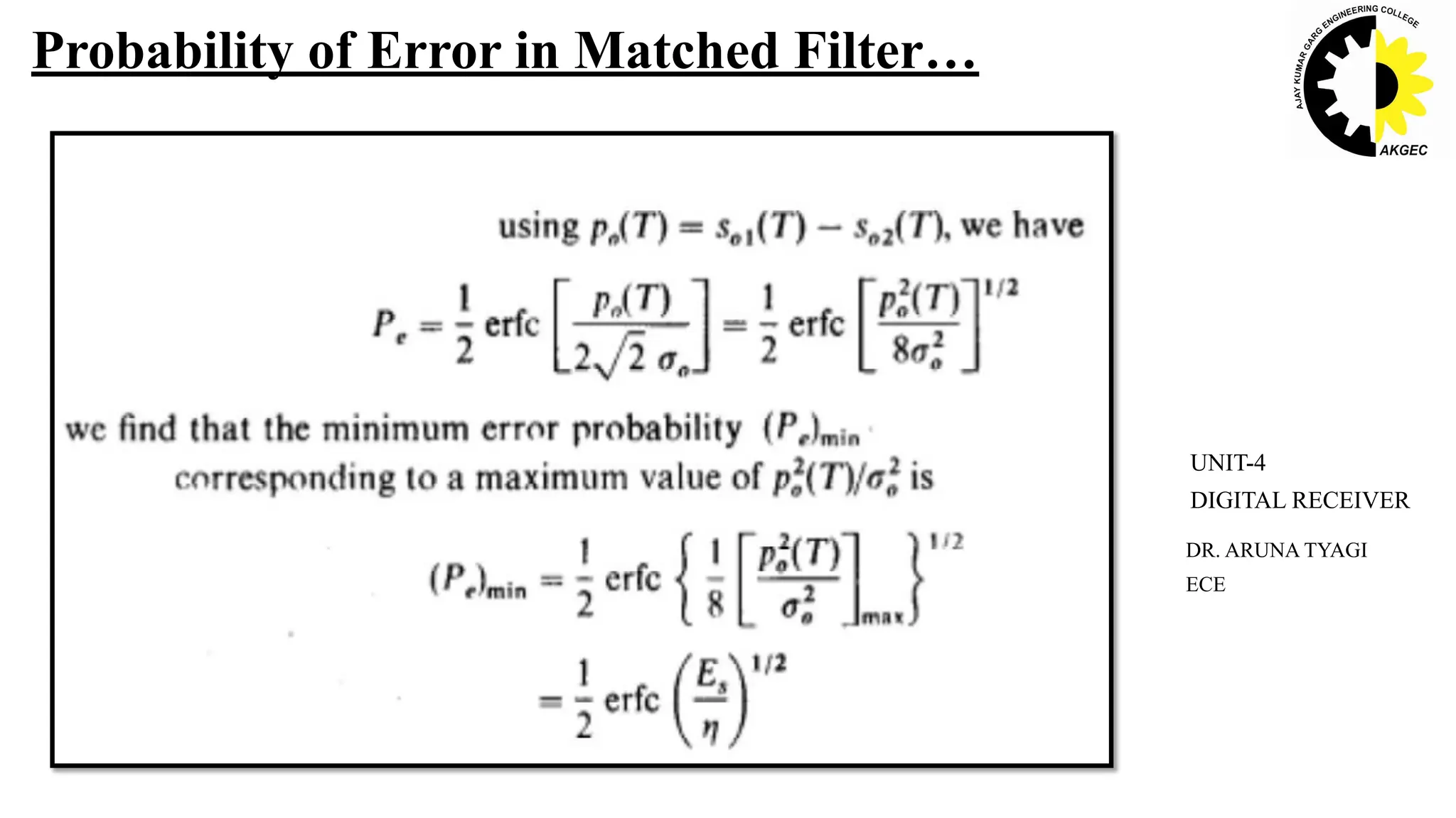
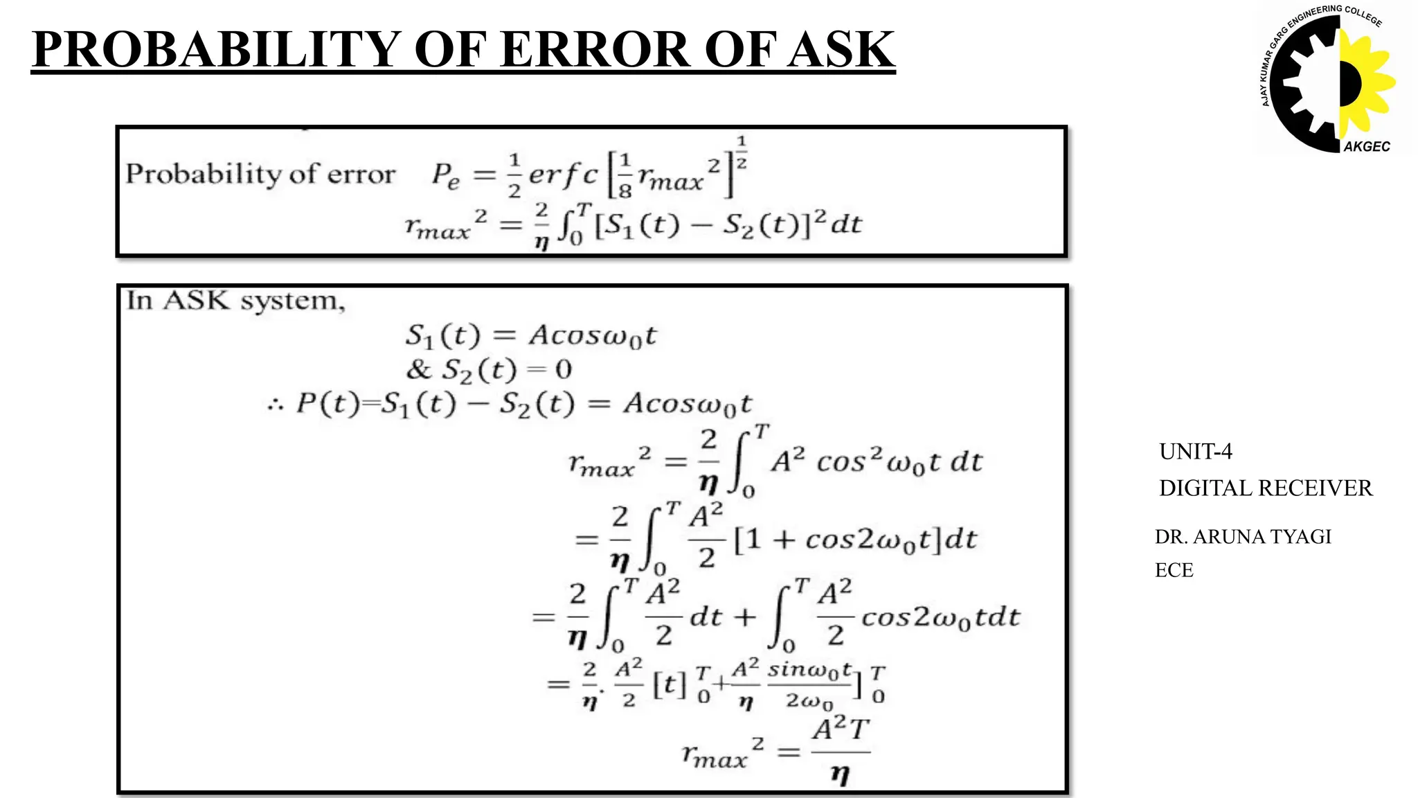
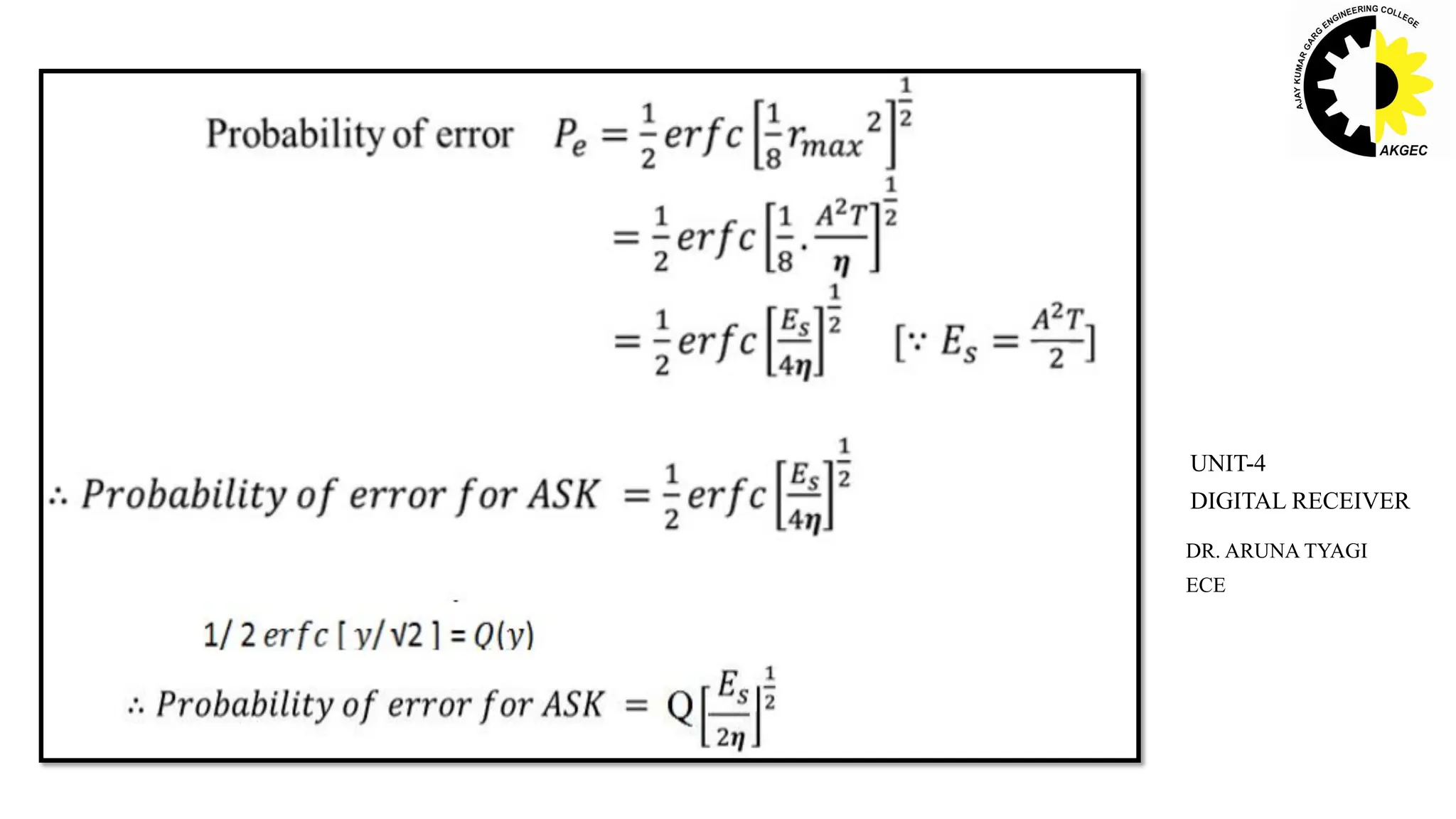
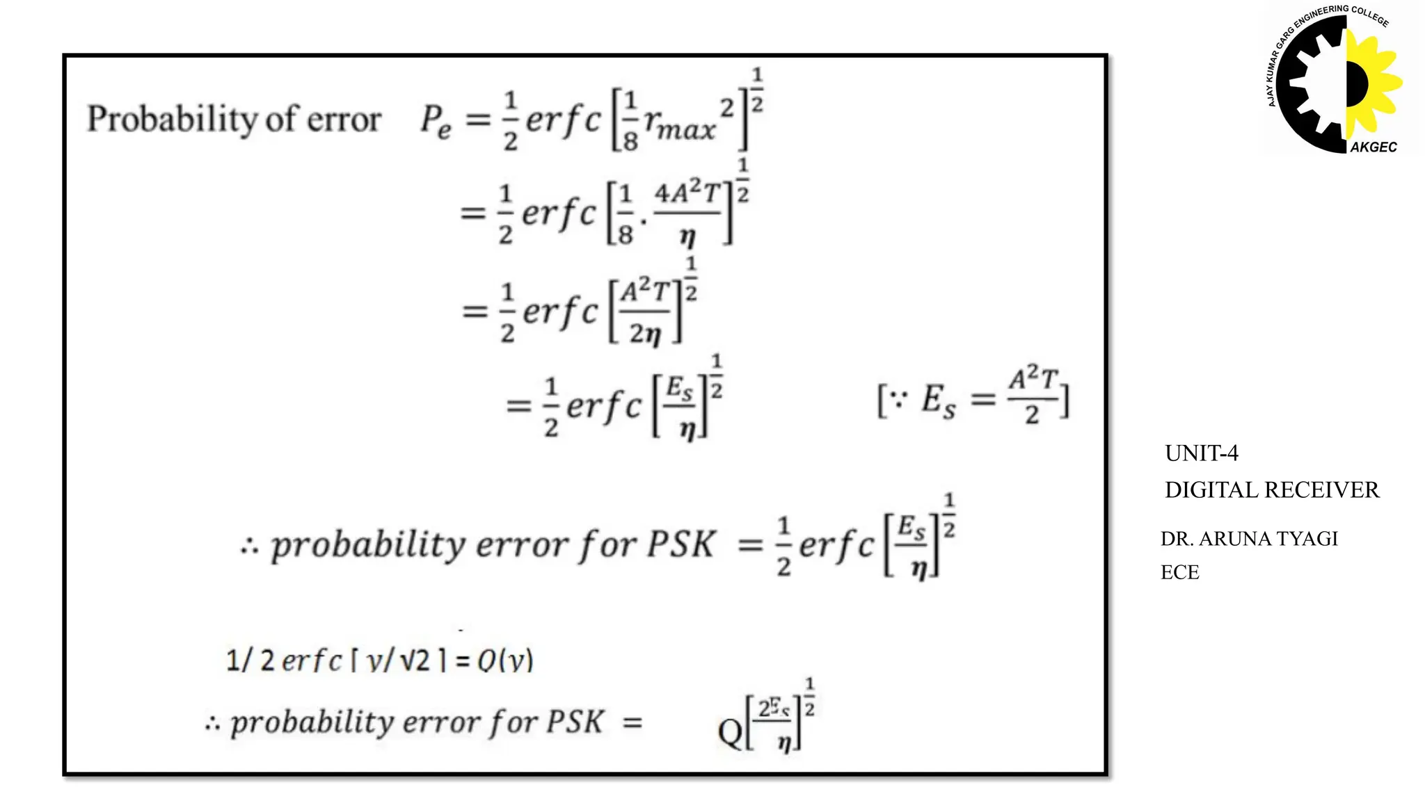
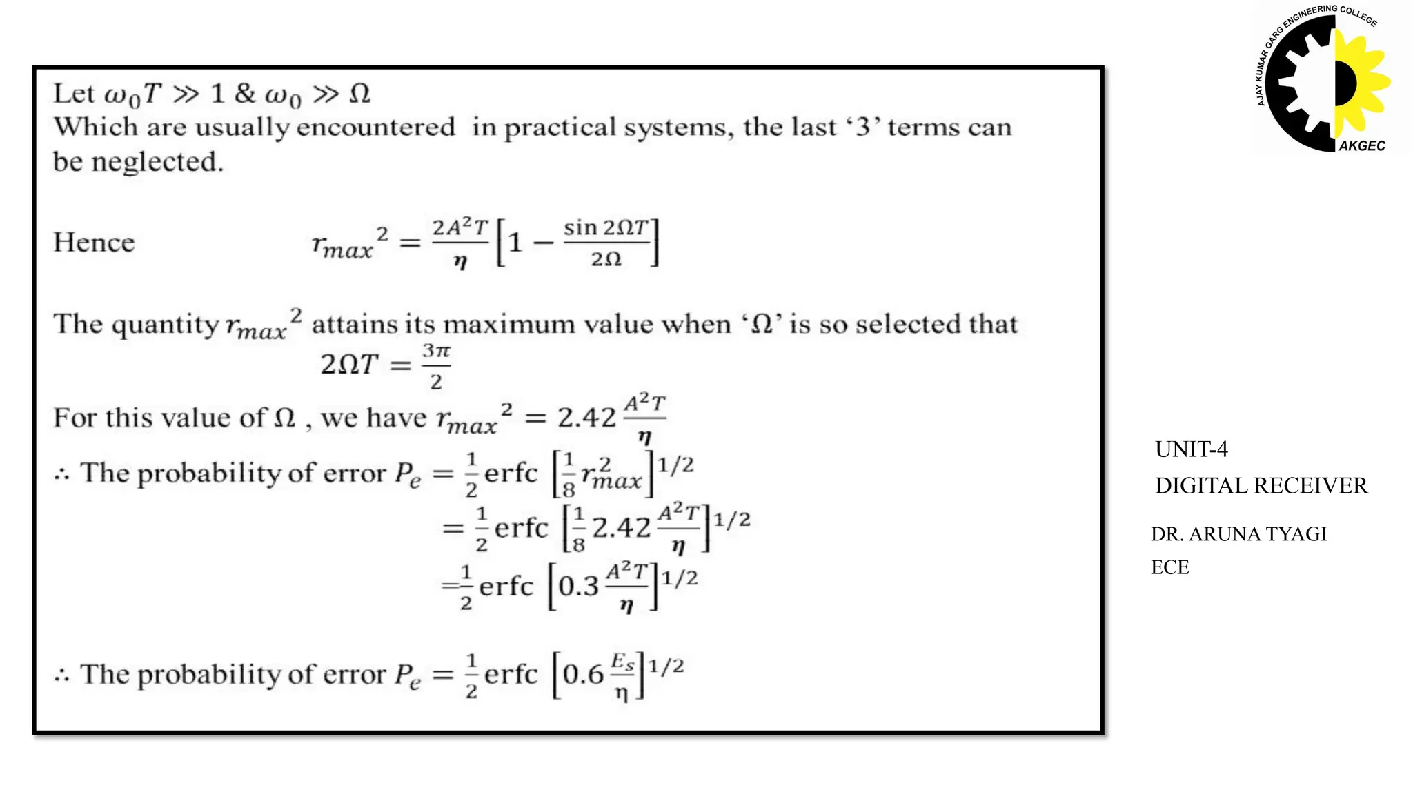
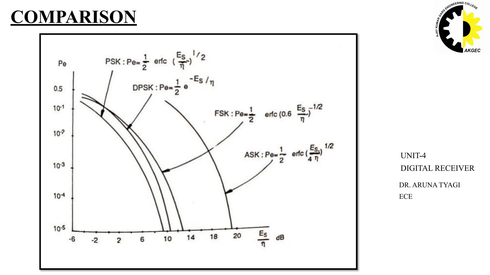
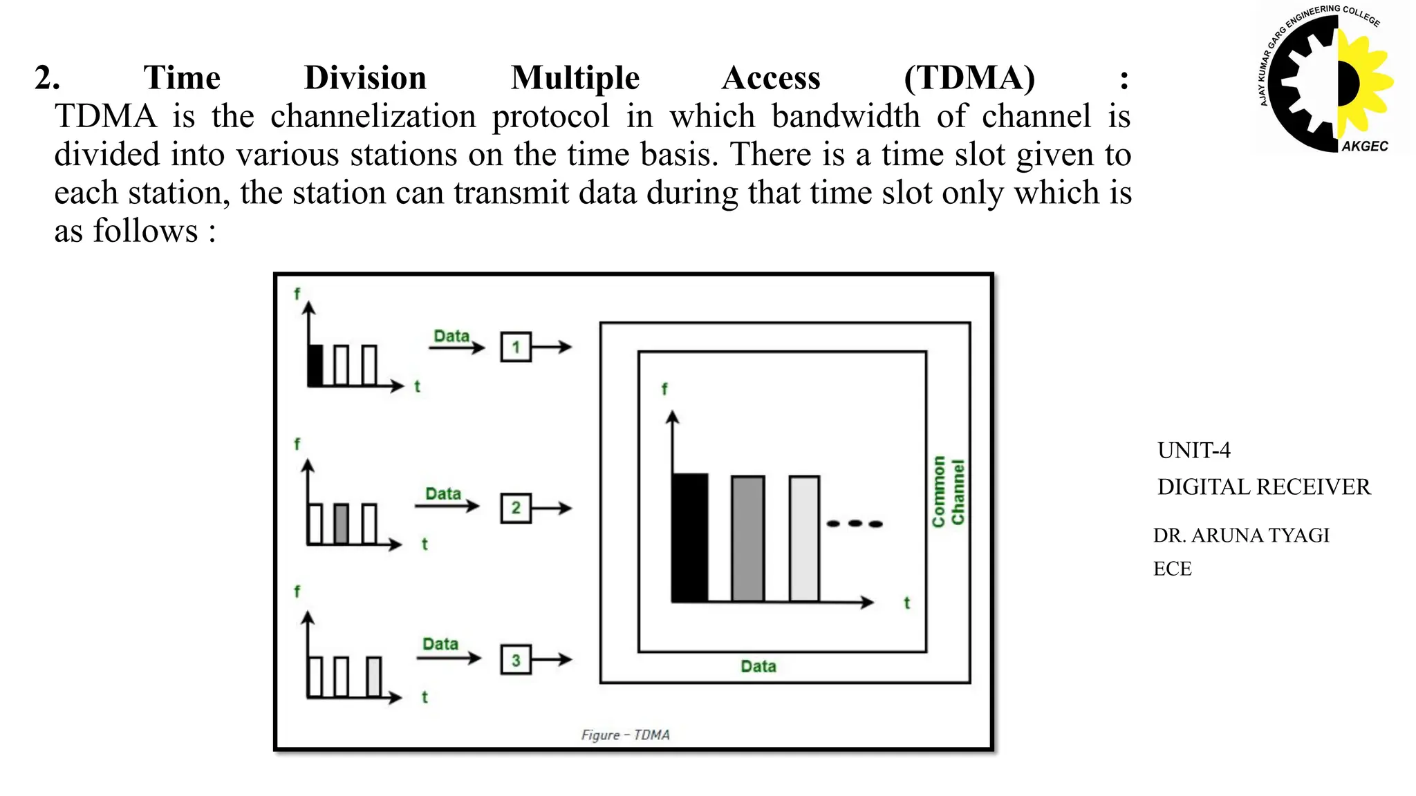
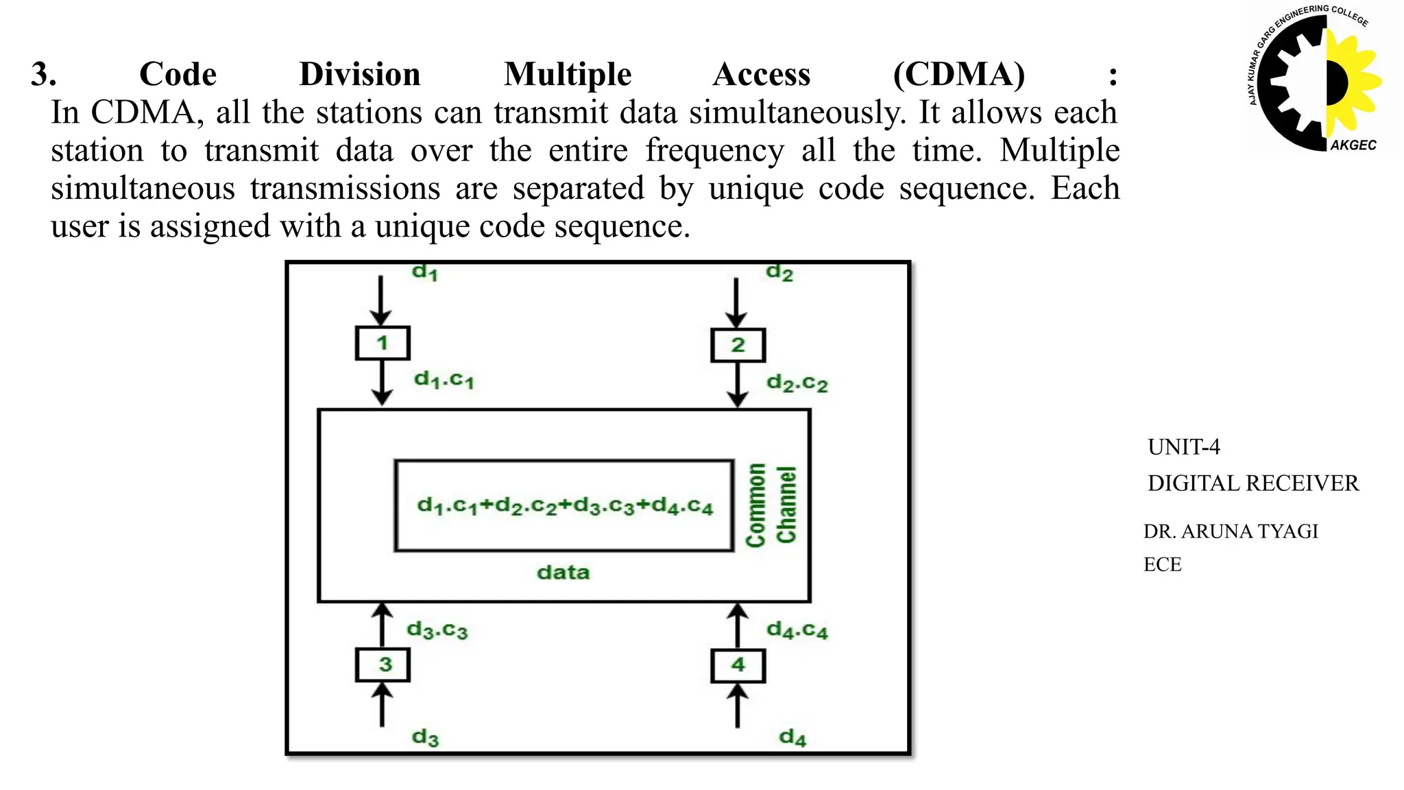
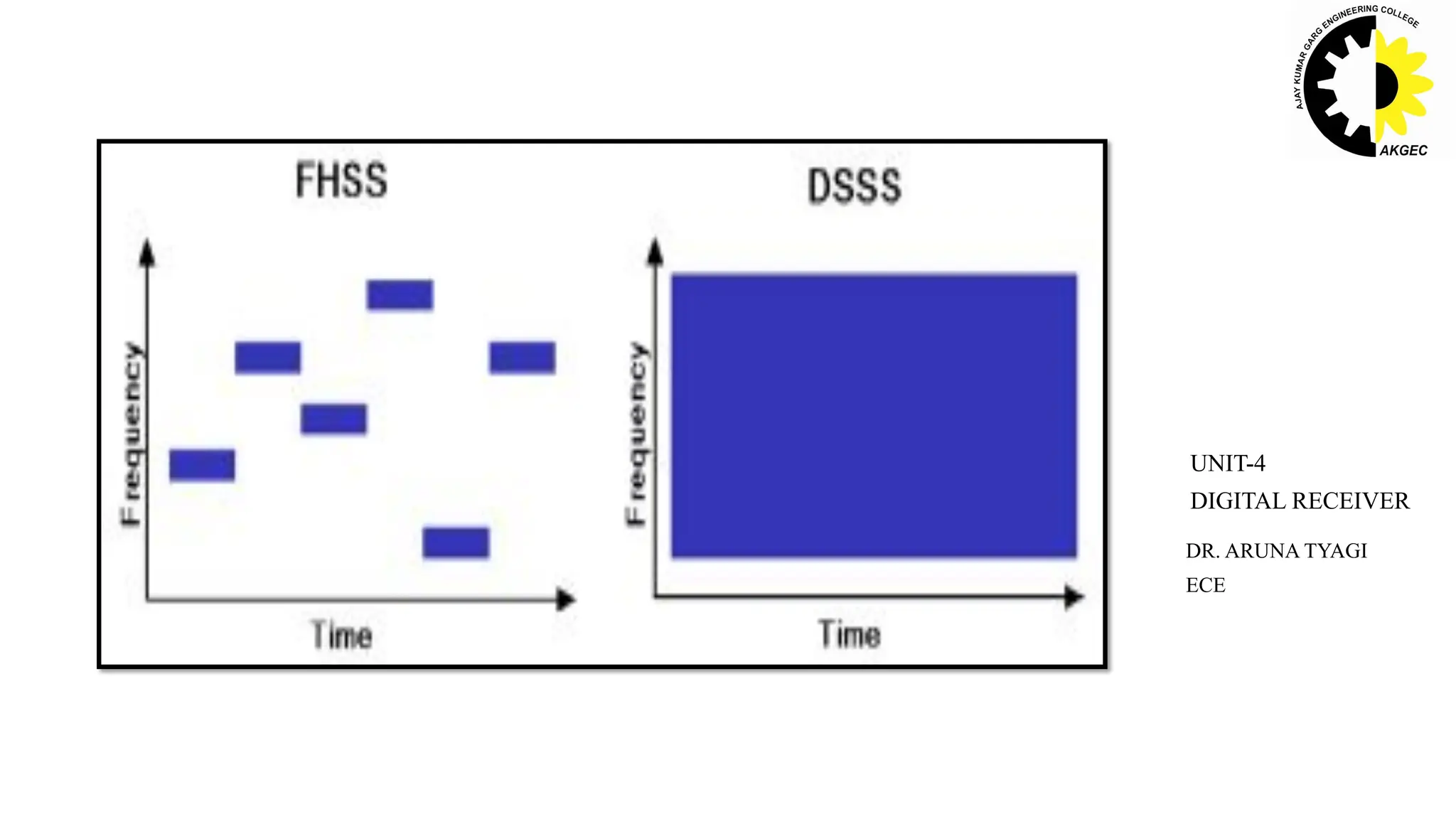
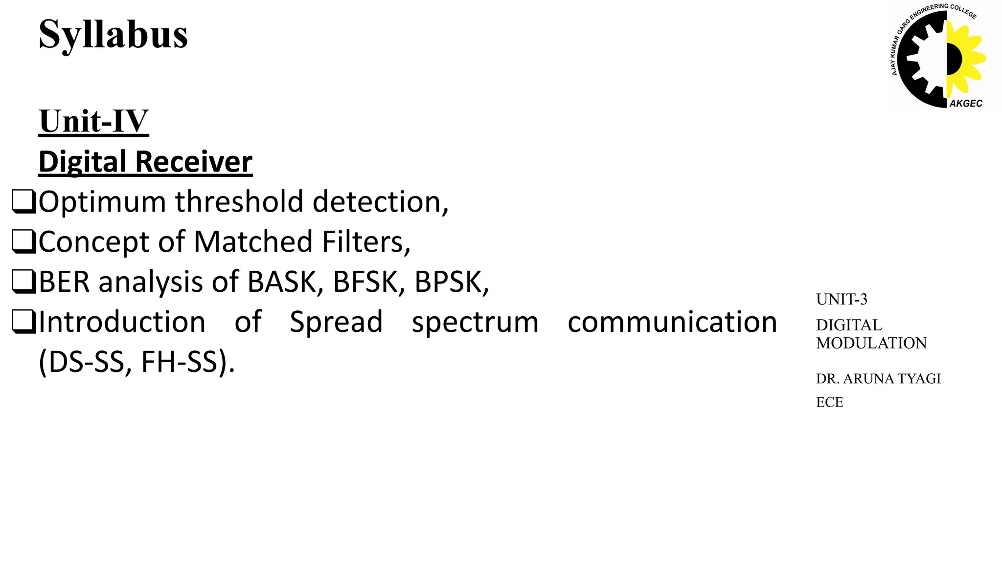
The document discusses various concepts related to digital receivers and signal processing, focusing on optimum threshold detection and matched filters. It explains the synchronization process in digital communication, the function of matched filters in maximizing signal-to-noise ratio, and introduces spread spectrum techniques for secure communication. Additionally, it covers the principles behind comparing signals and the importance of coding in spread-spectrum technologies.
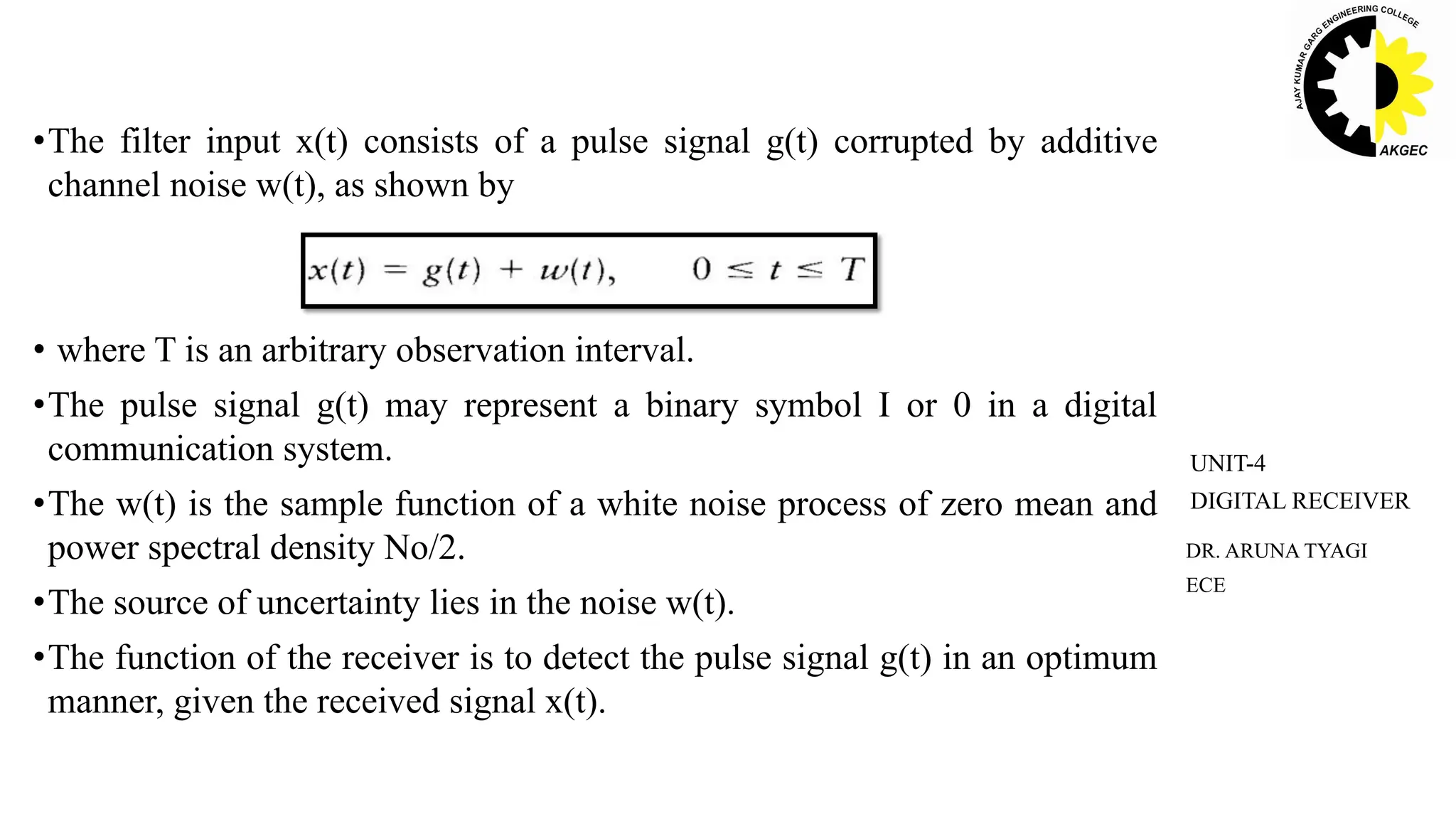
![As it is well known, we determine the distance of a target by
transmitting a pulse (say x[n]) and detecting the return. The time interval
between transmission and reception gives the information on the
distance of the target. The figure below illustrates the problem
DR. ARUNA TYAGI
ECE
UNIT-4
DIGITAL RECEIVER](https://image.slidesharecdn.com/dcunit4-240624180120-1417d648/75/DC-Unit-chapter-containing-information-about-electronic-8-2048.jpg)