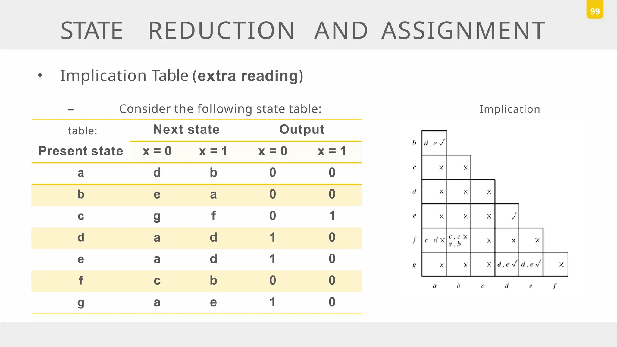
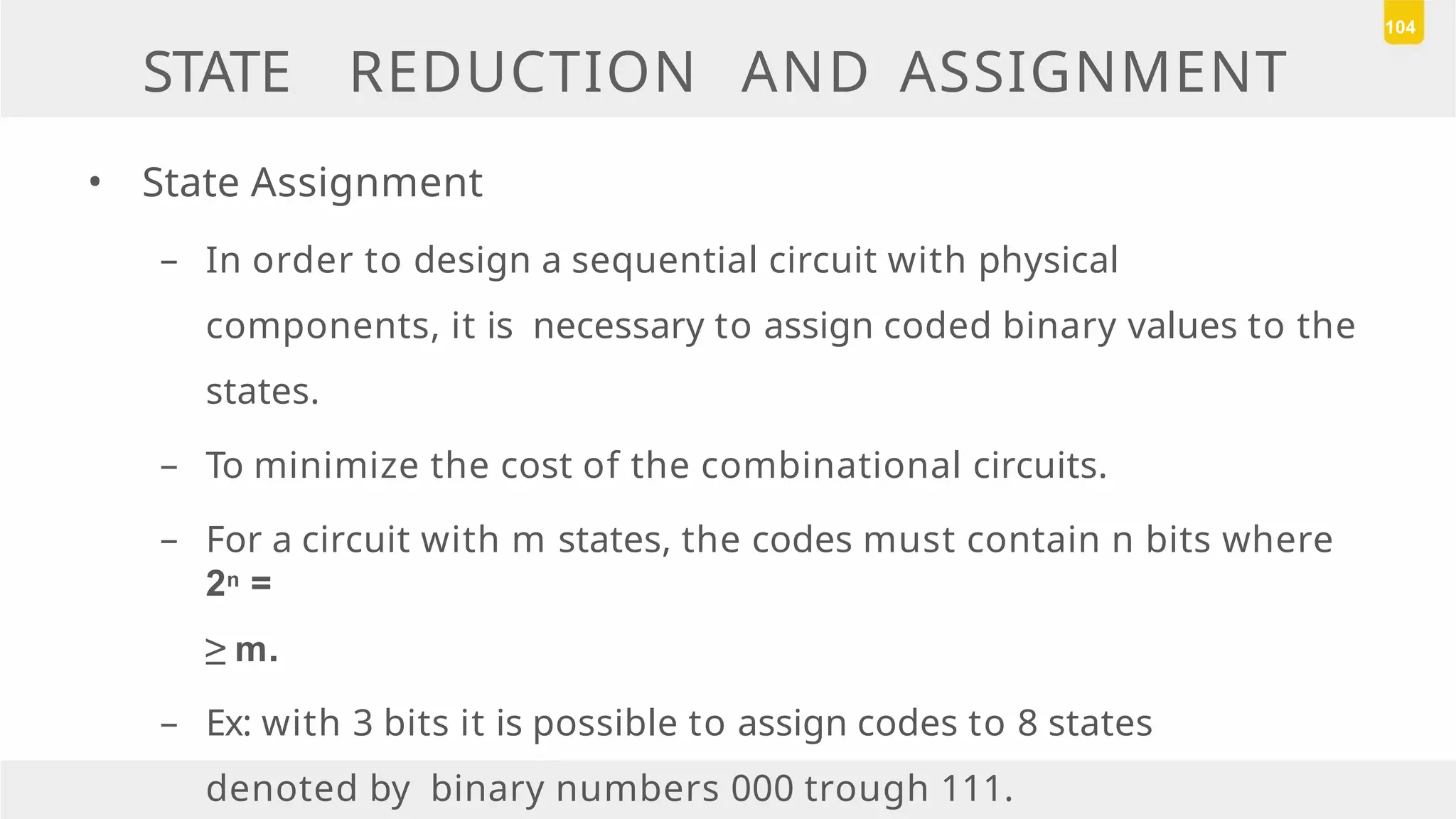
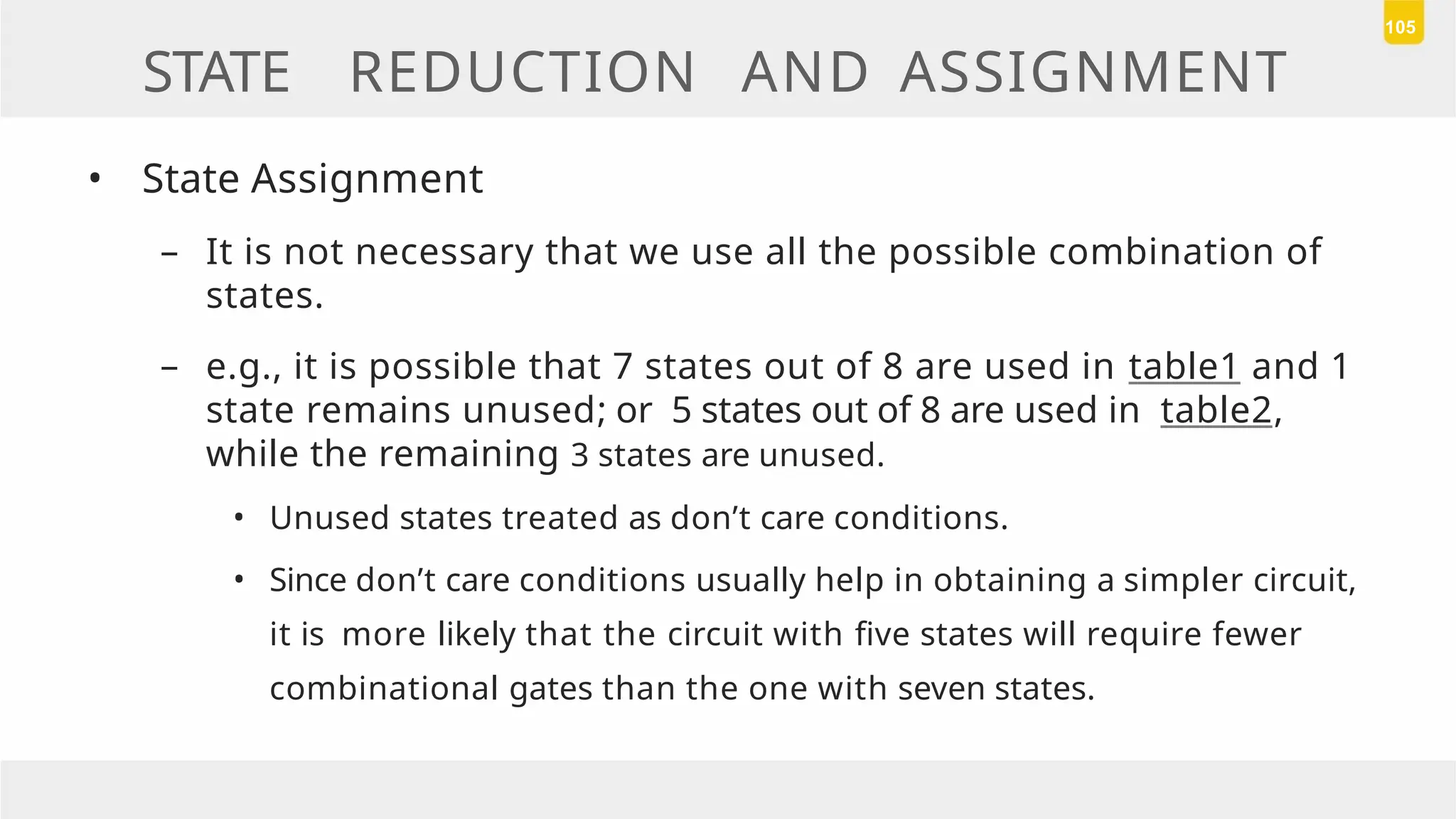
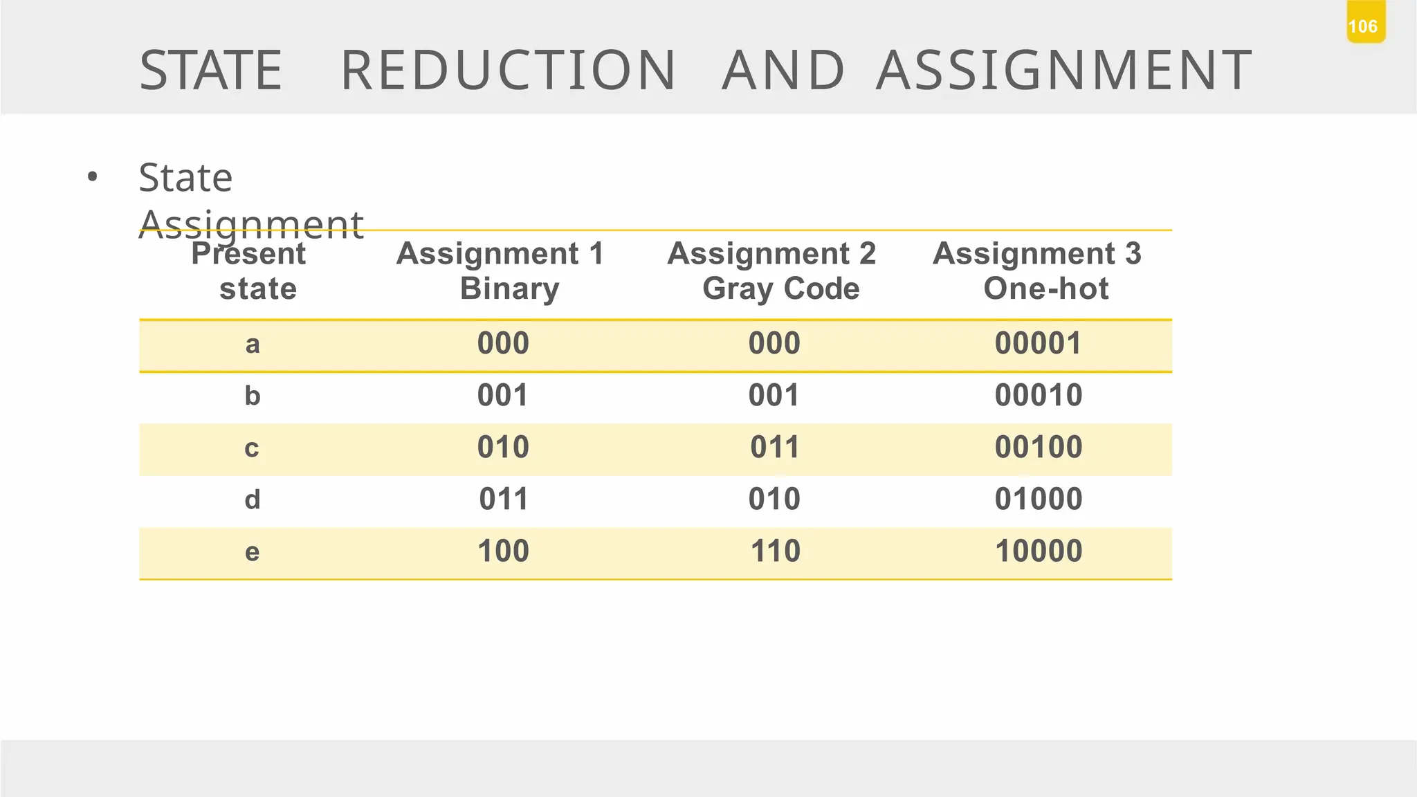
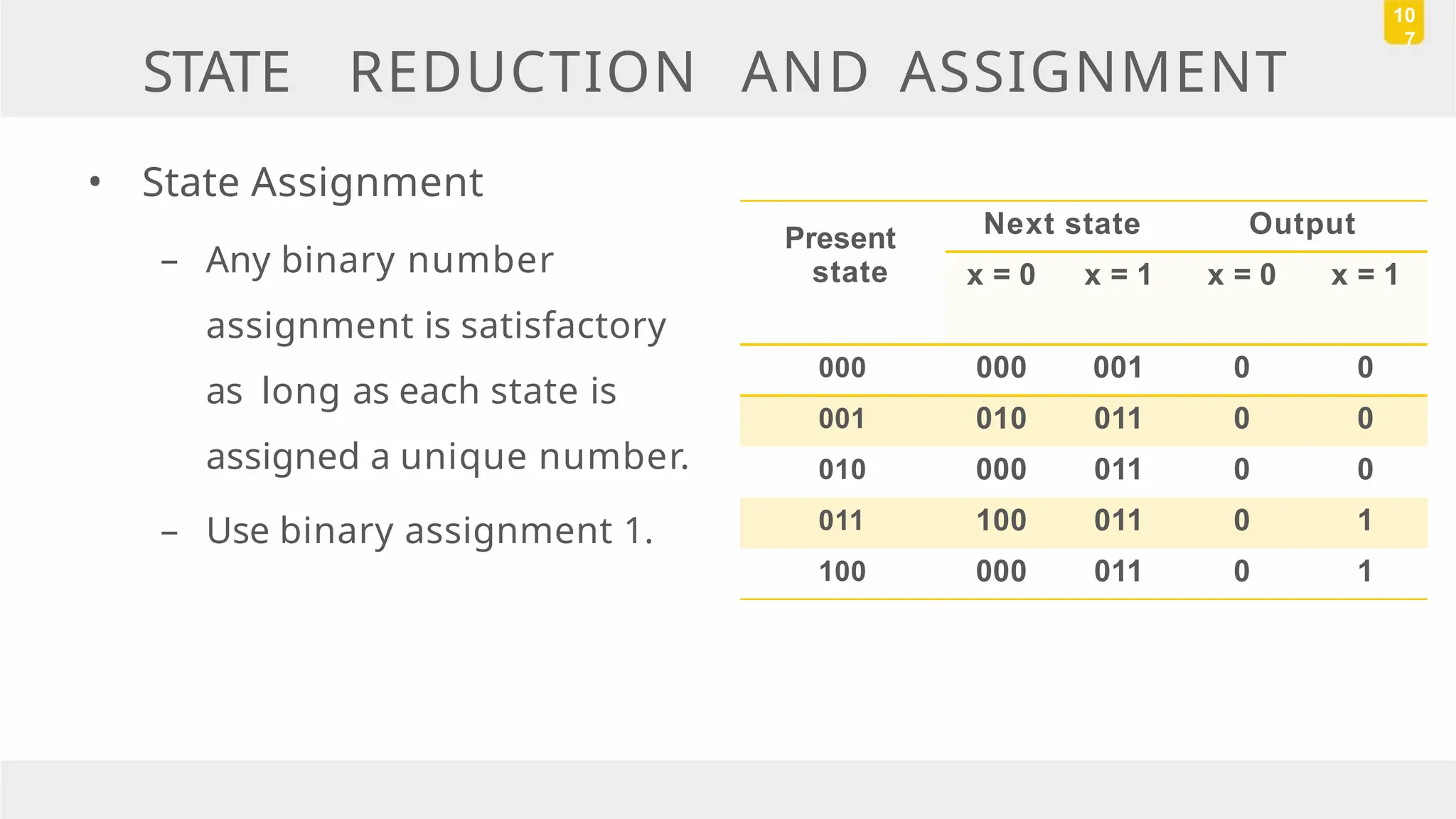
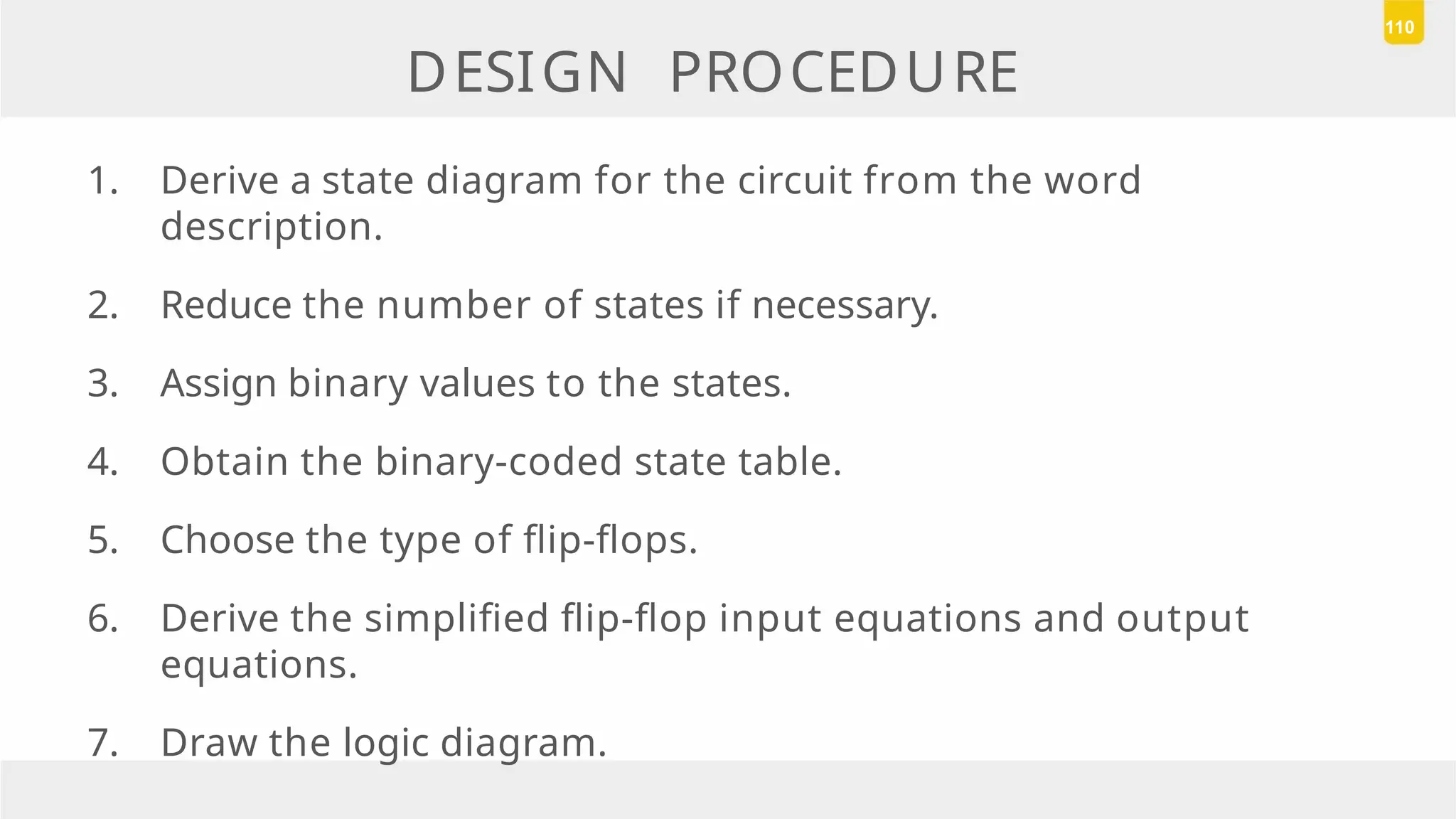
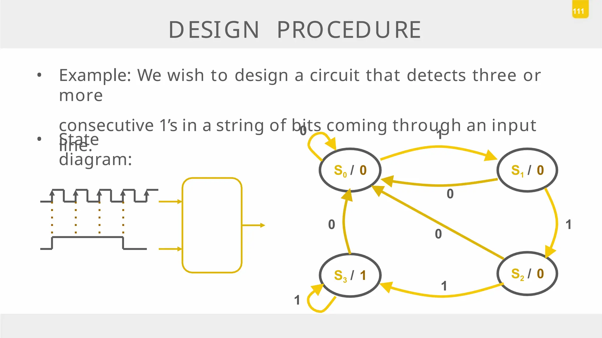
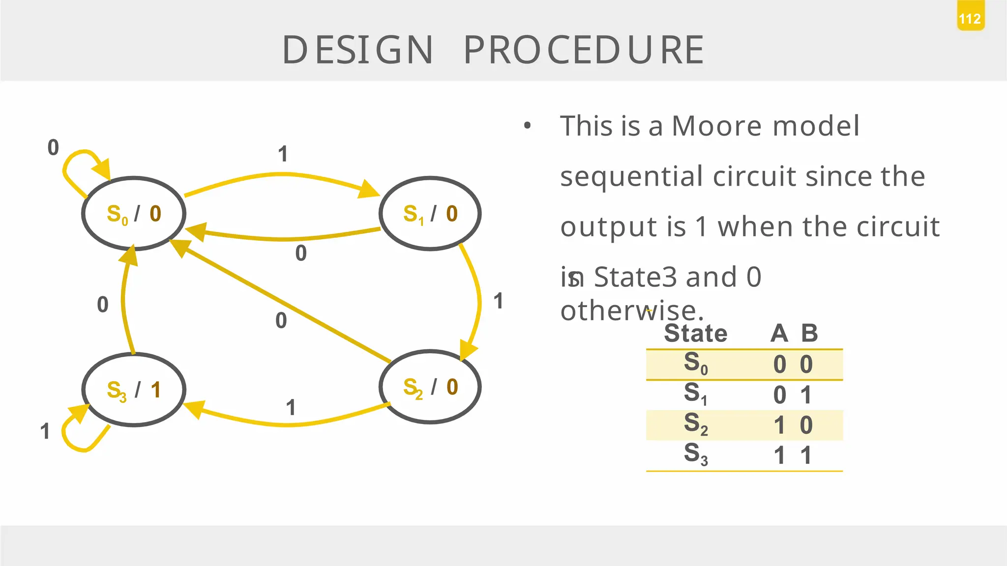
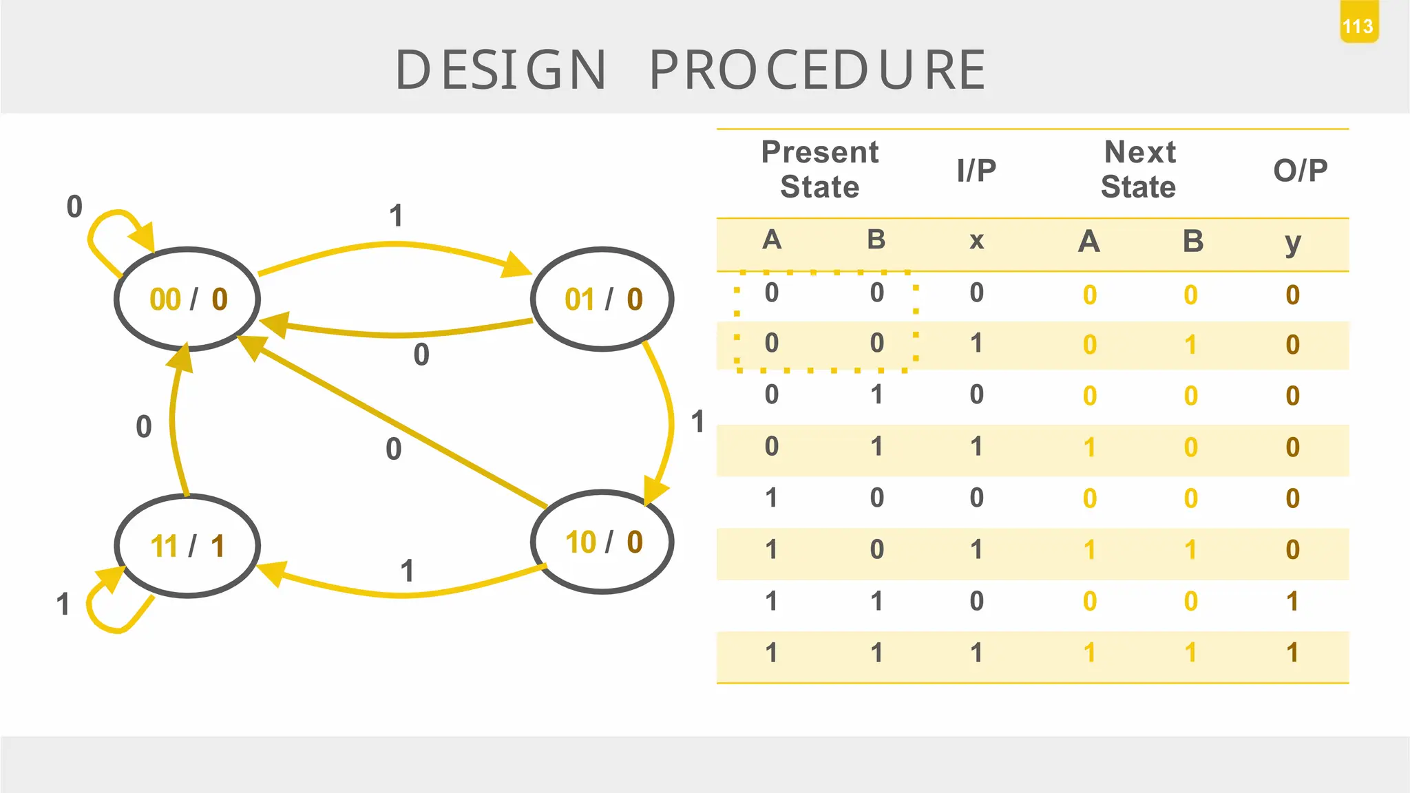
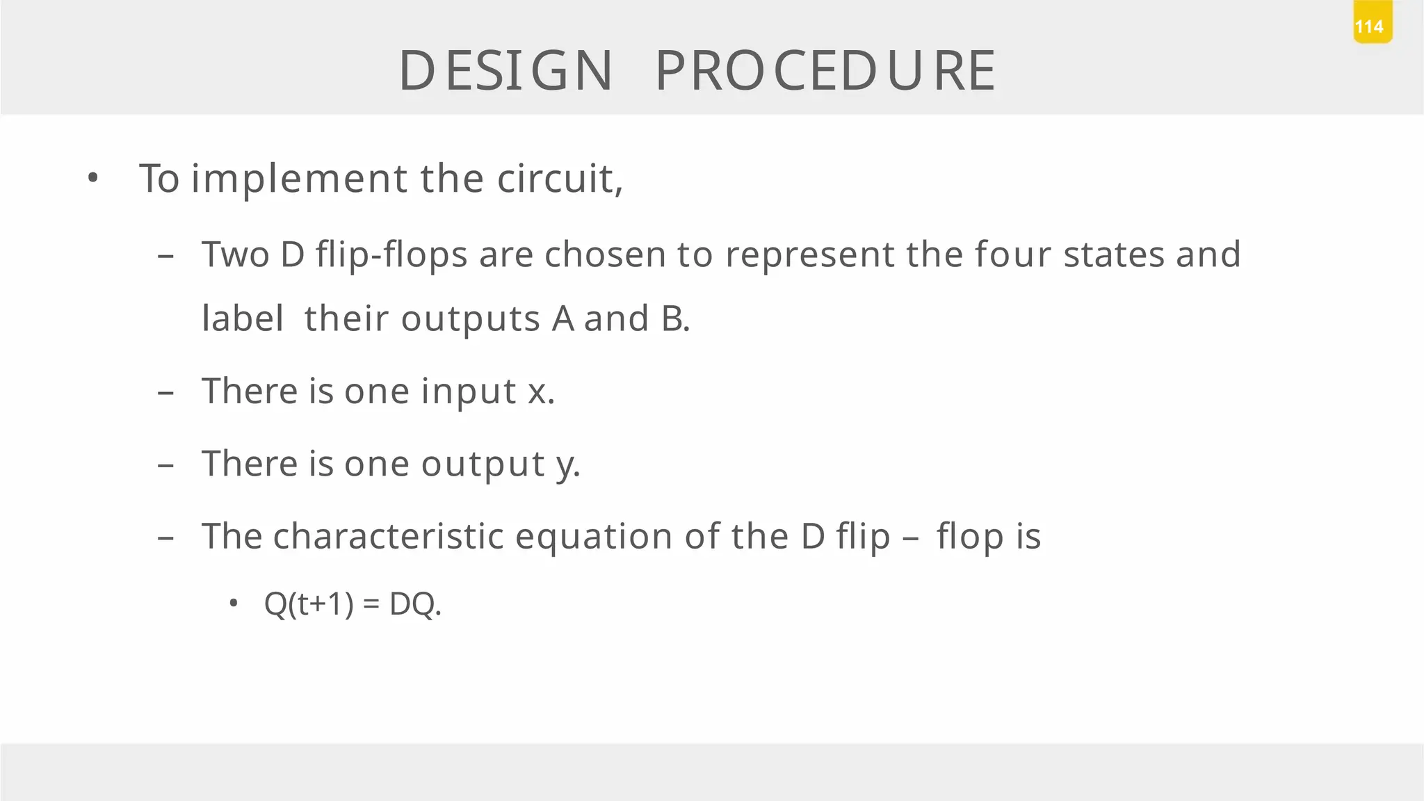
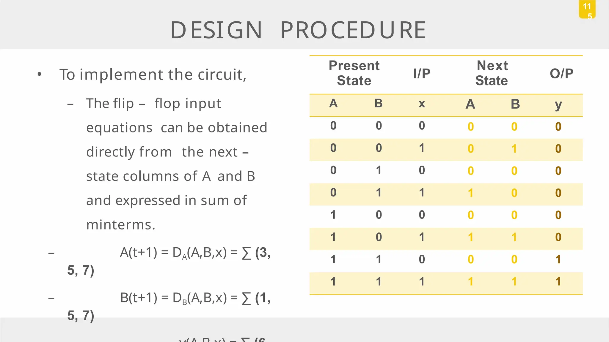
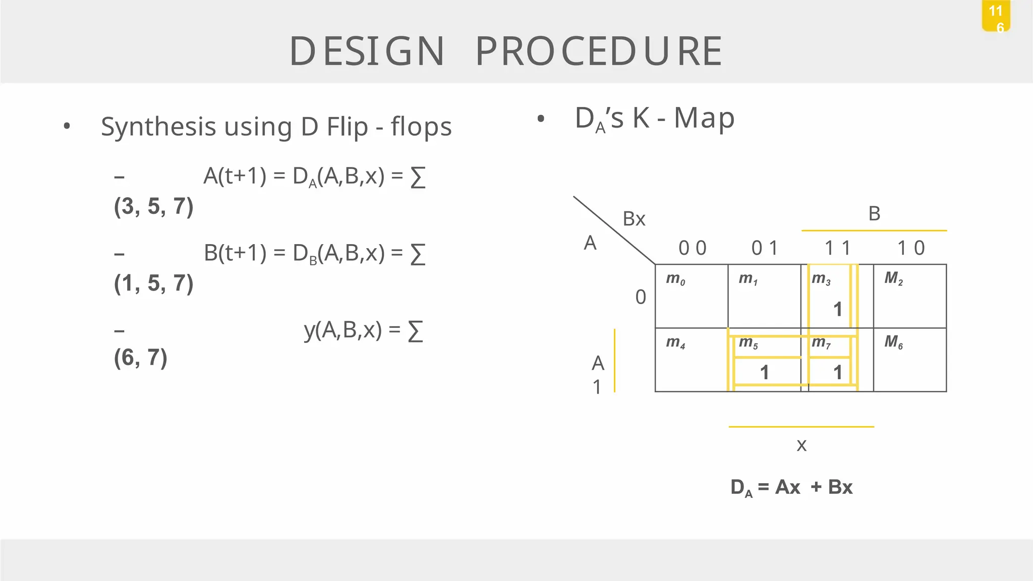
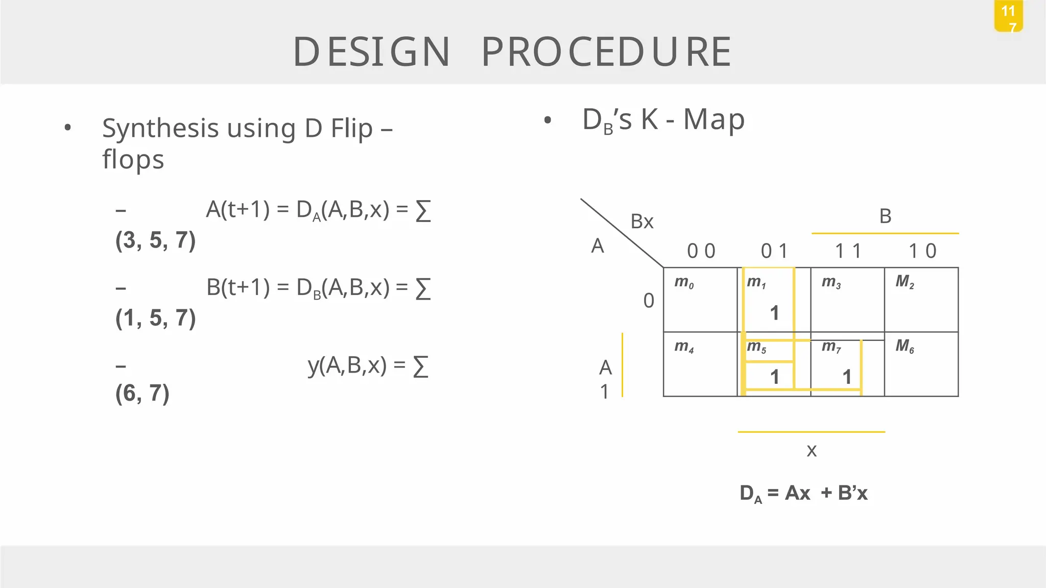
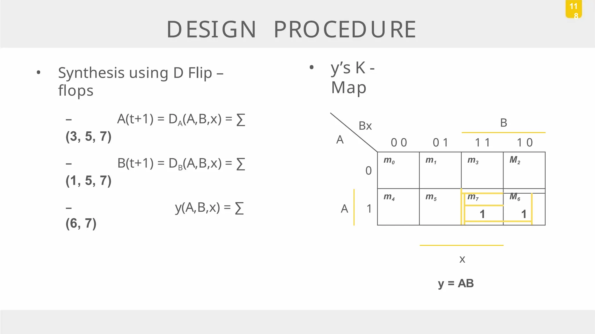
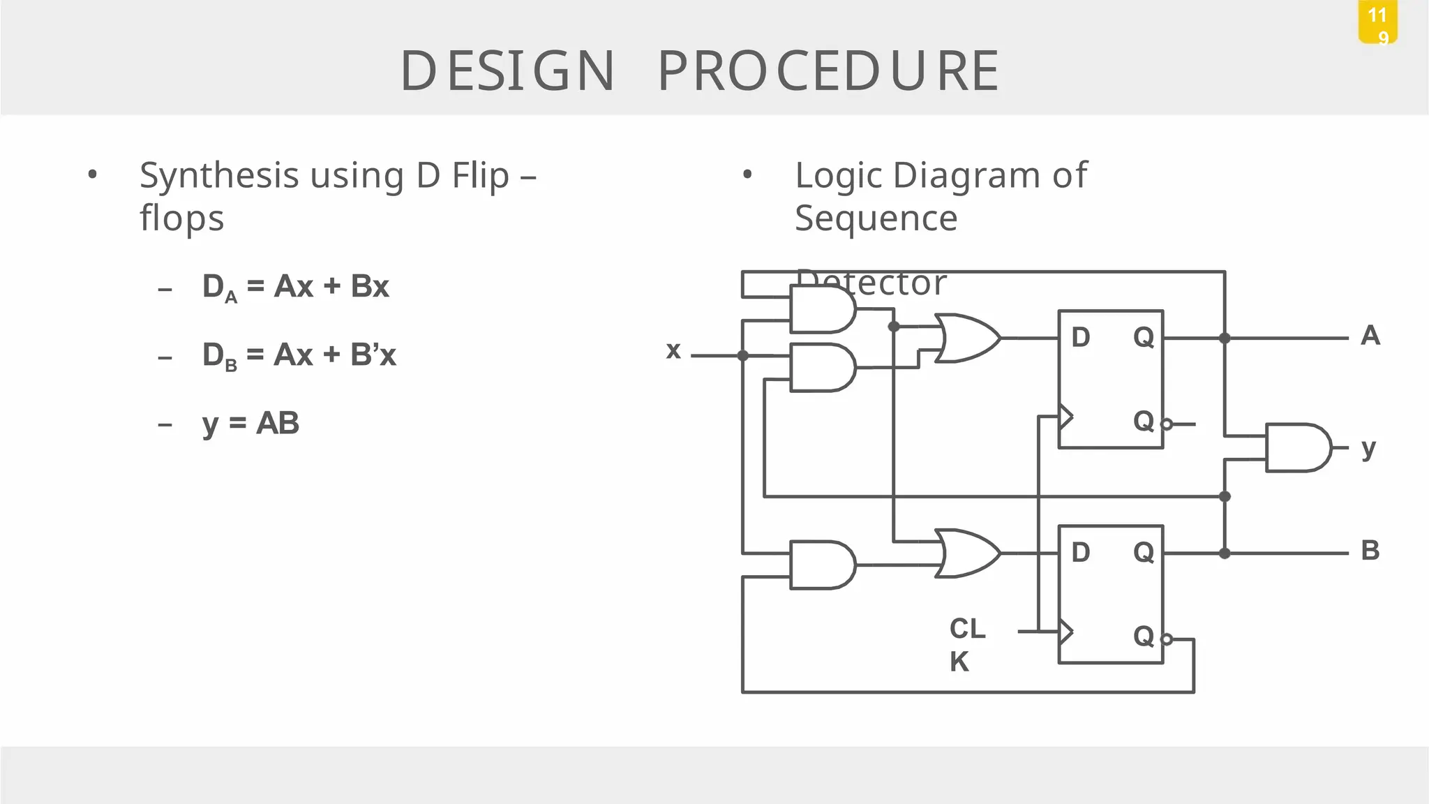
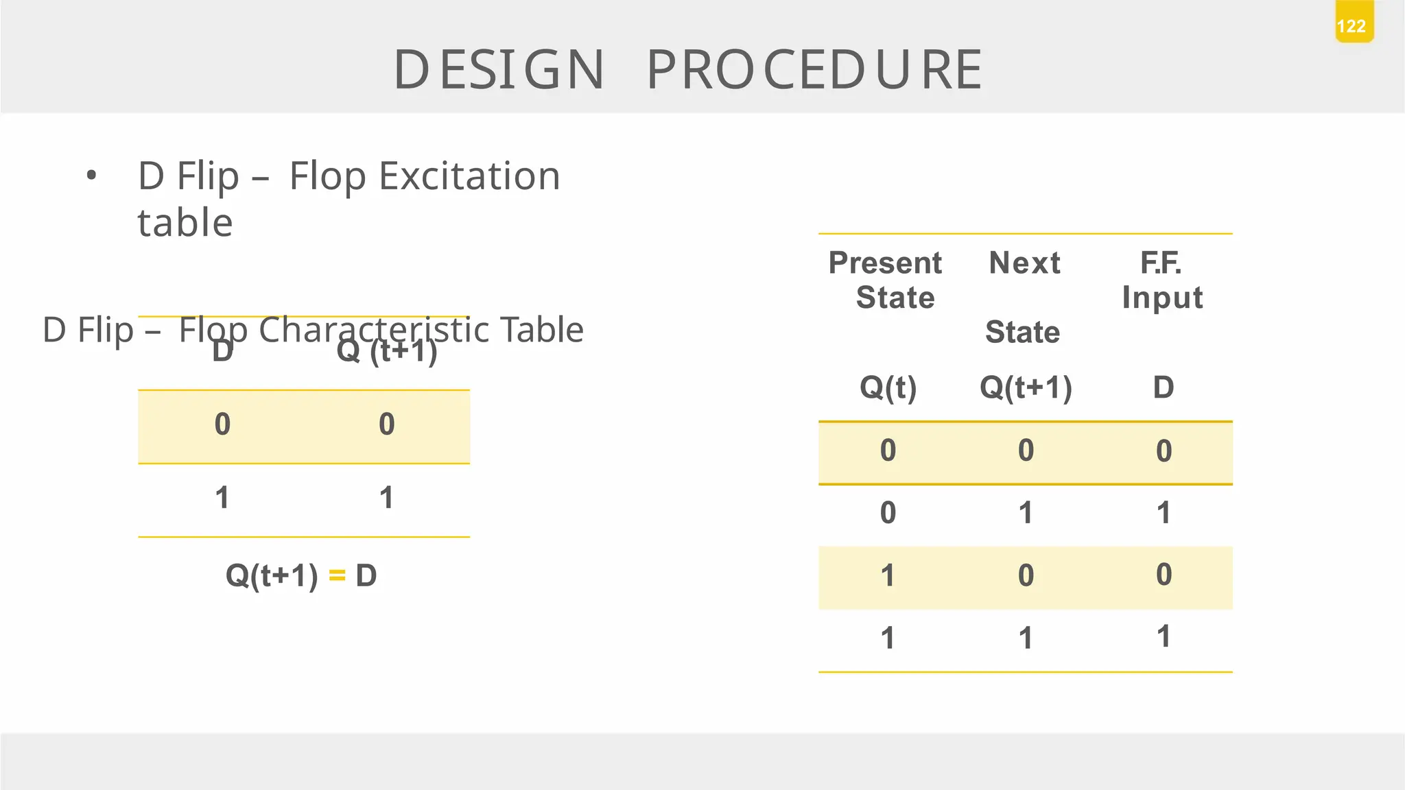
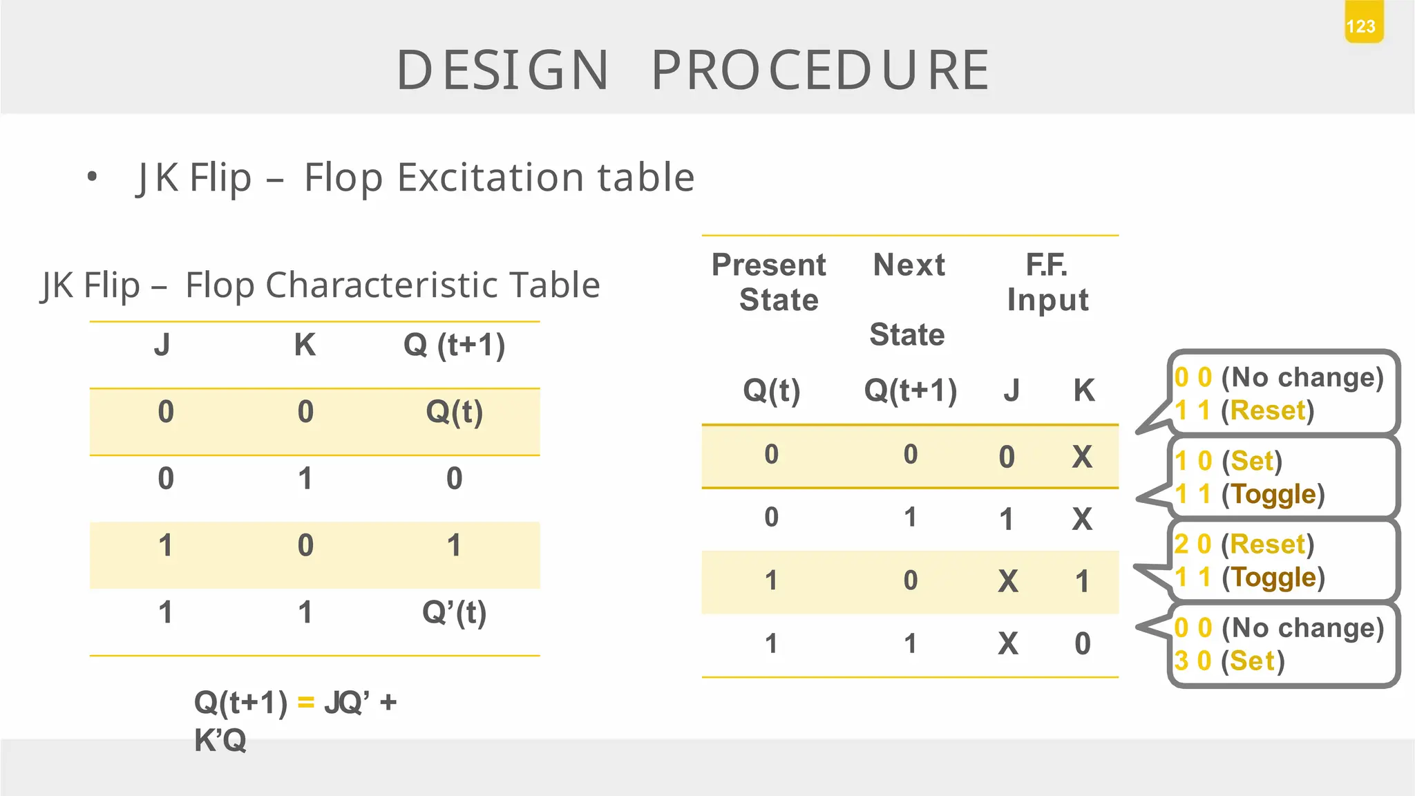
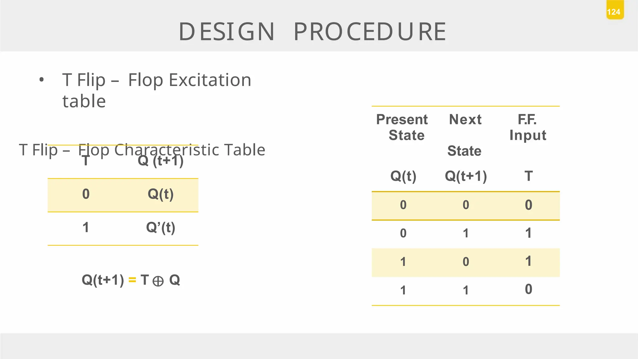
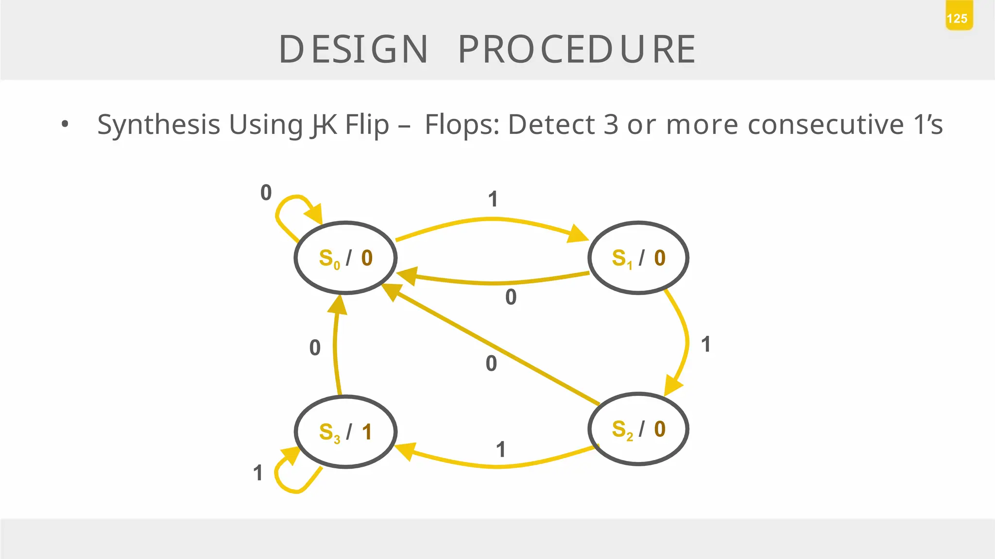
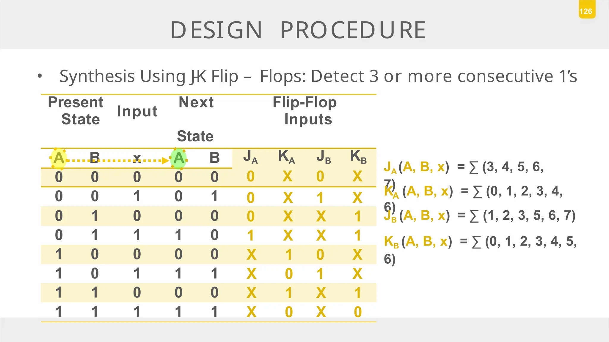
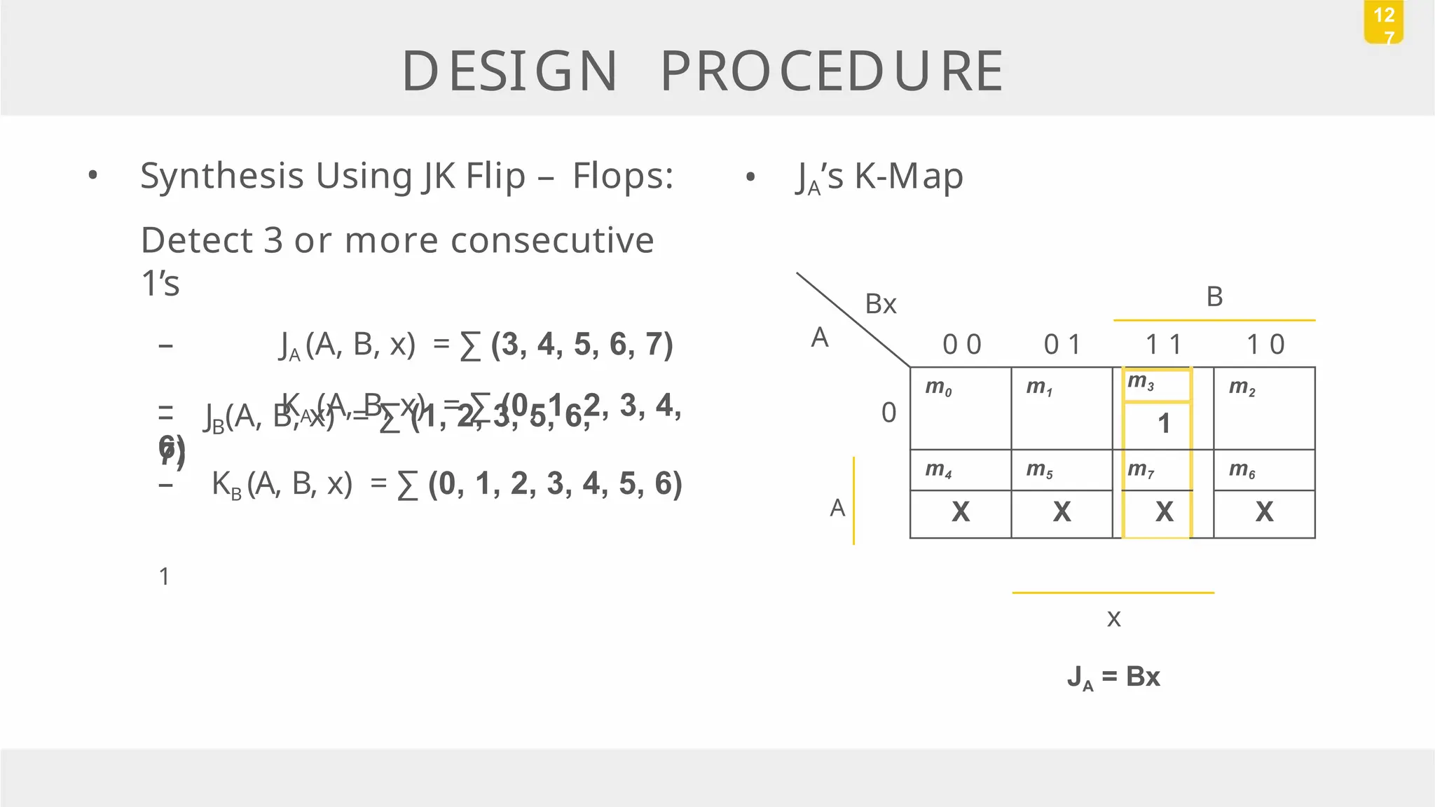
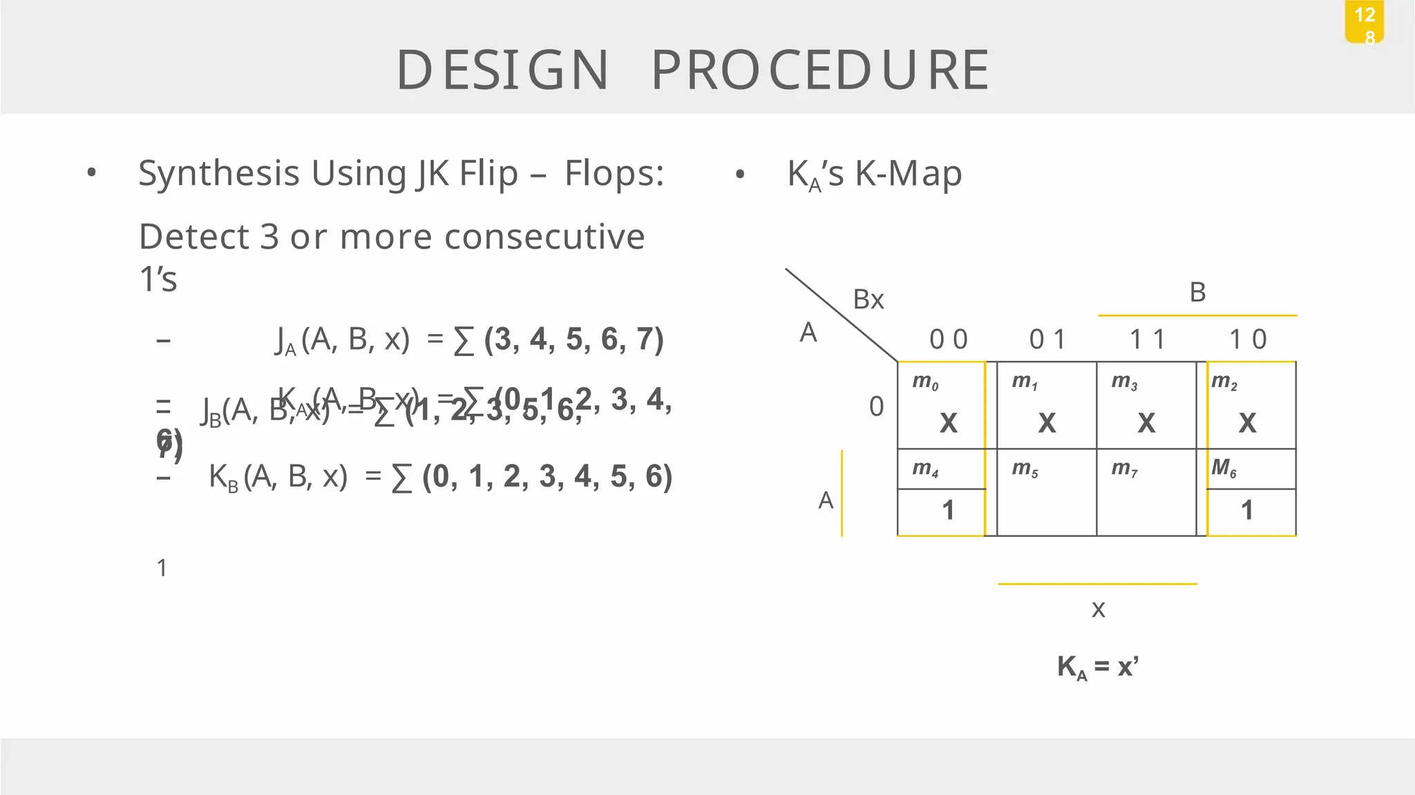
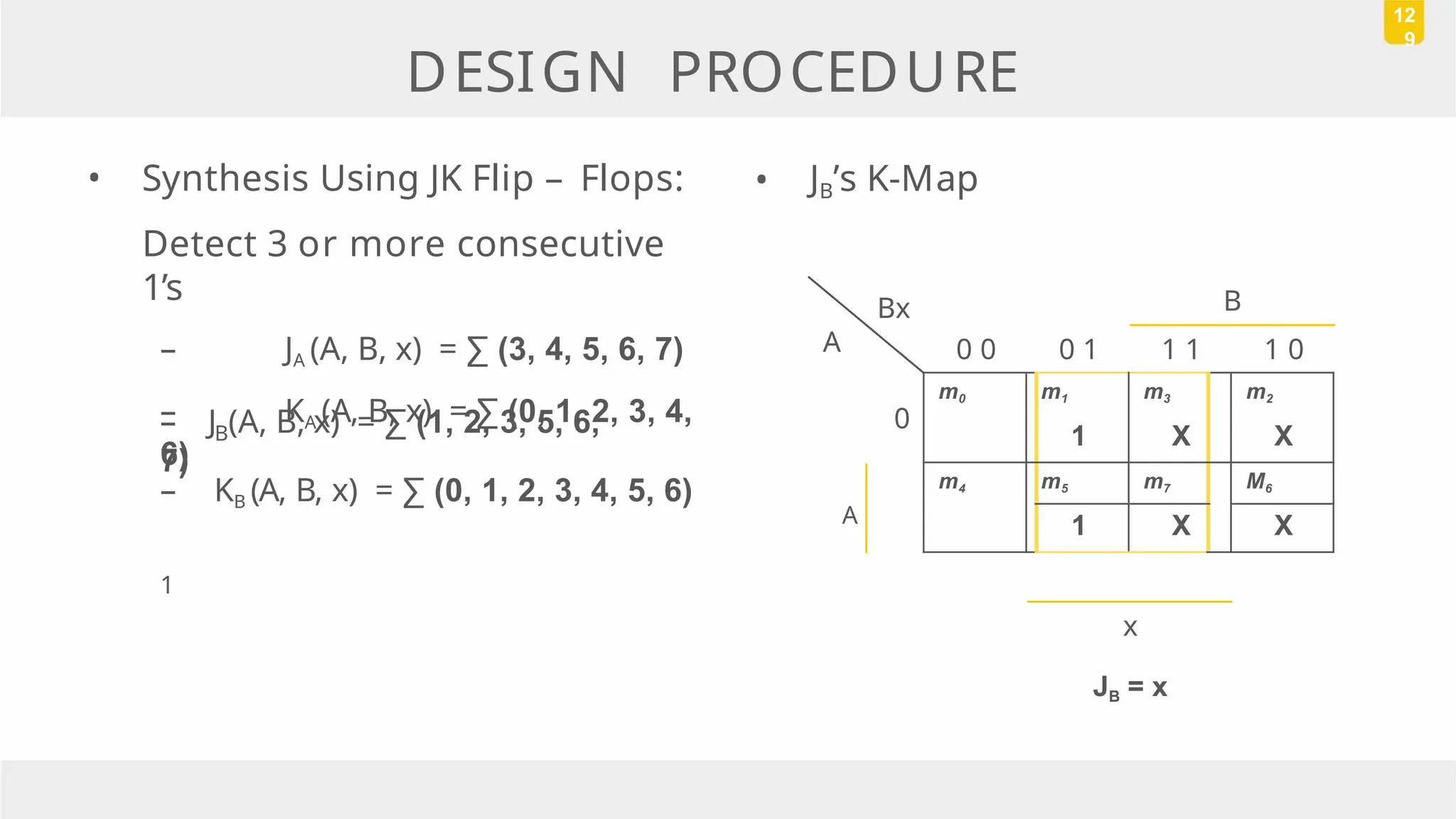
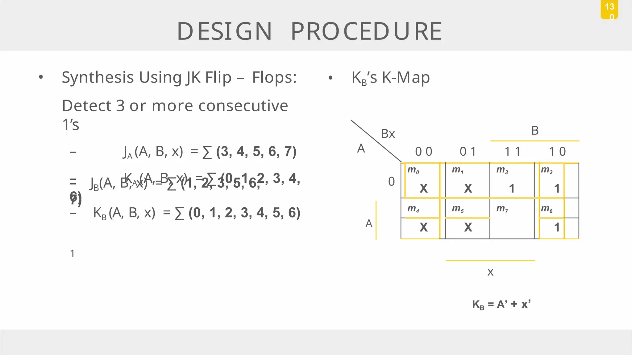
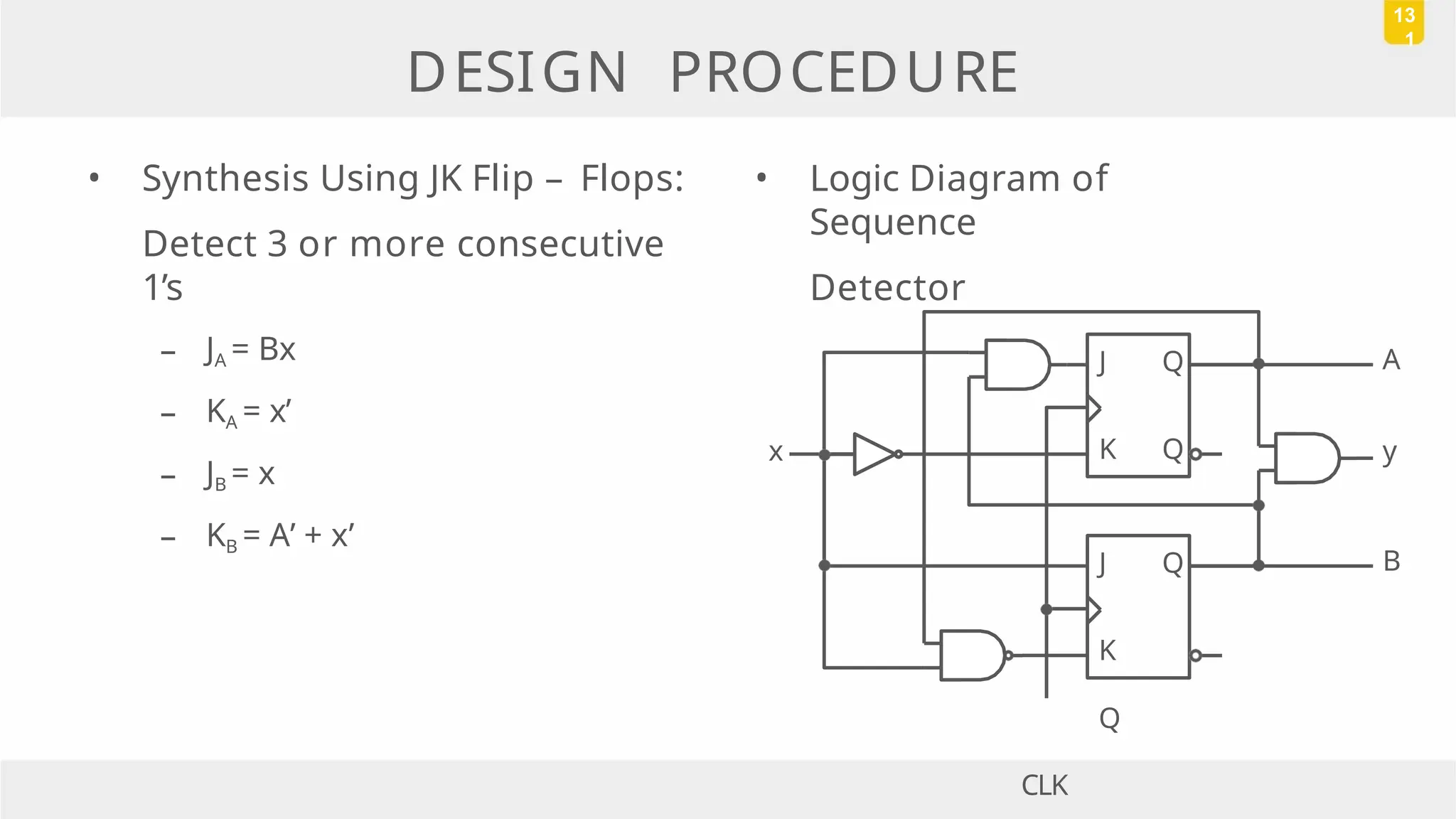
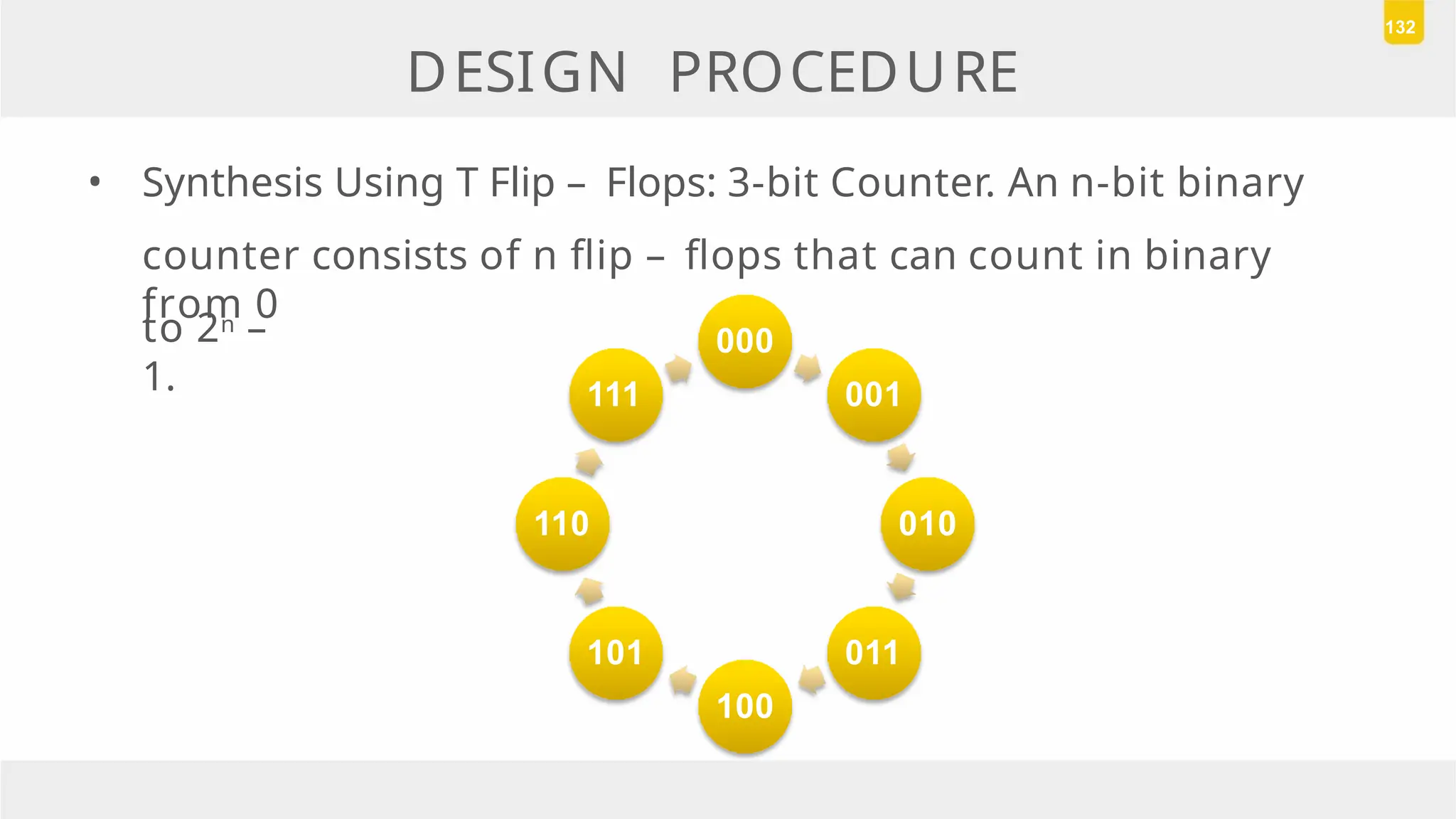
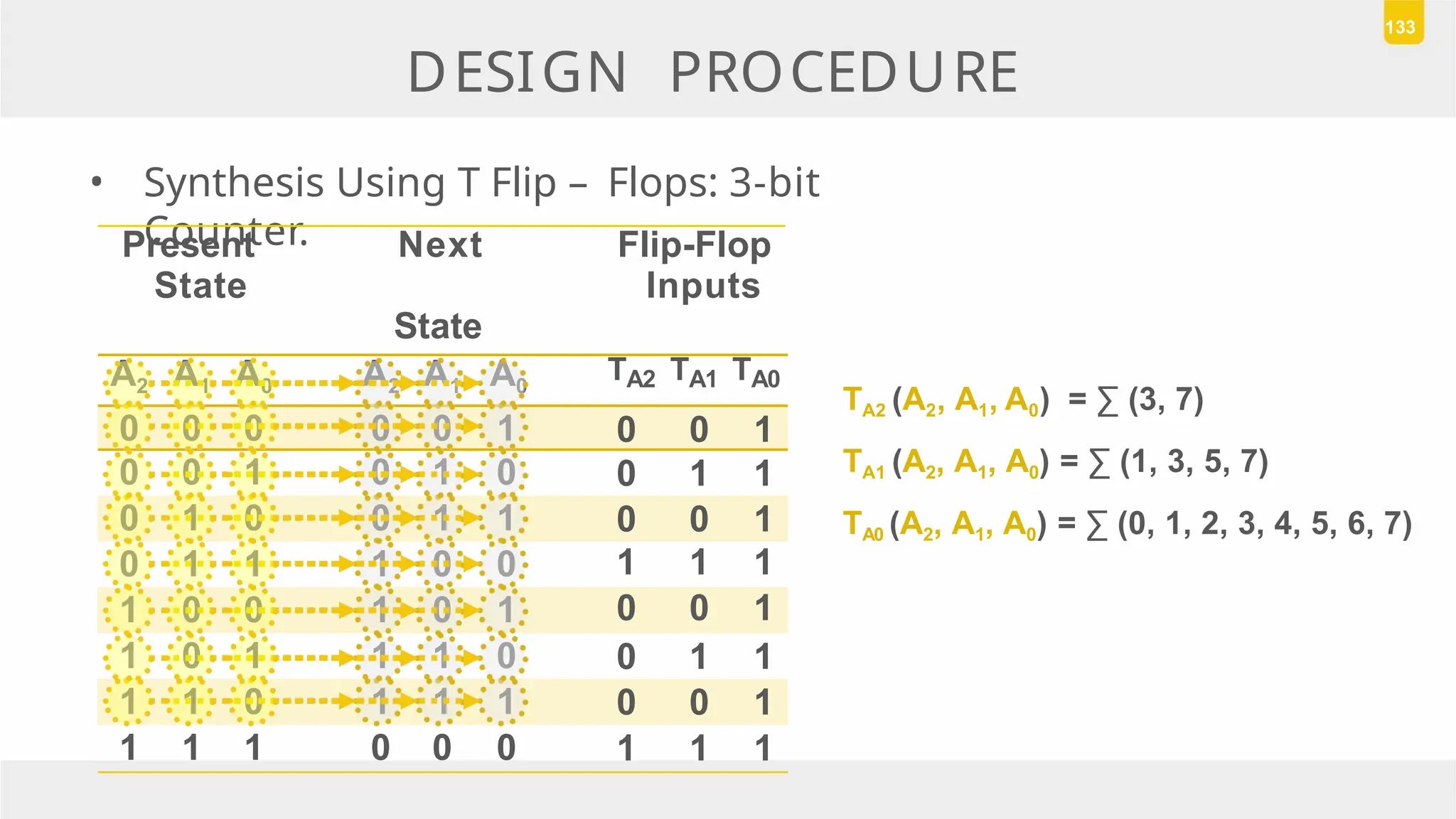
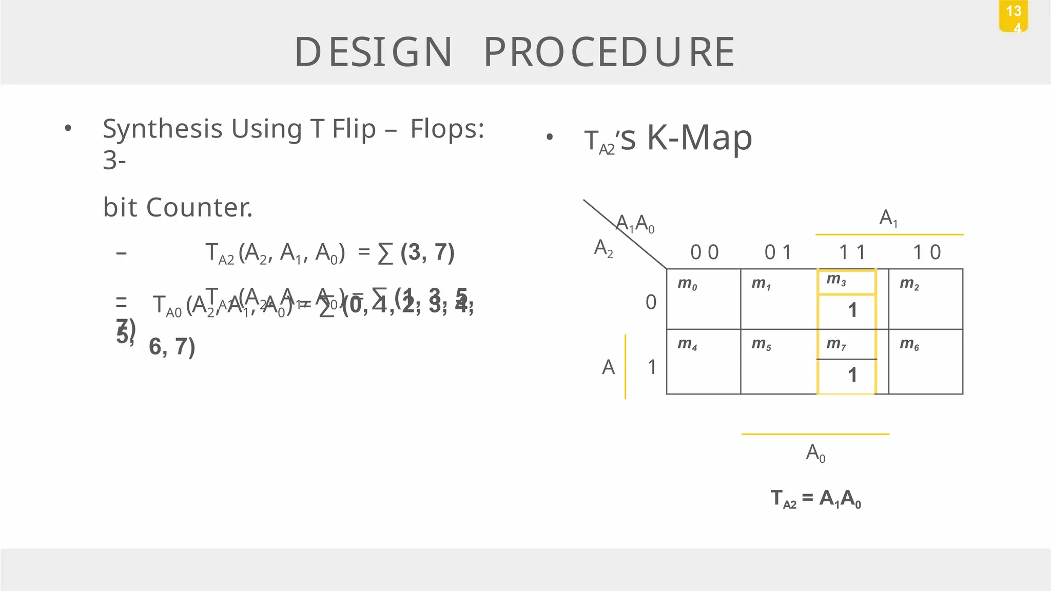
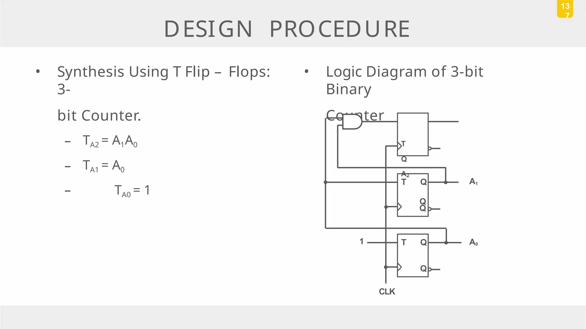
Sequential Circuits
STATE REDUCTION AND ASSIGNMENT
• Reduce the number of states
– Checking of each pair of states for possible equivalence can be
done systematically using Implication Table.
– Unused states are treated as don't-care condition  fewer
combinational gates.
95
STATE REDUCTION AND ASSIGNMENT
• Implication Table (extra reading)
– The state-reduction procedure for completely specified state tables is
based on the algorithm that two states in a state table can be
combined into one if they can be shown to be equivalent.
-- There are occasions when a pair of states do not have the same next
states, but, nonetheless, go to equivalent next states.
96
STATE REDUCTION AND ASSIGNMENT
• Implication Table (extra reading)
Systematically checking of each pair of states for possible equivalence in a
table with a large number of.
 Chart that consists of squares: one for every possible pair of states,
that provide spaces for listing any possible implied states.
98
STATE REDUCTION AND ASSIGNMENT
99
Next state Output
Present state x = 0 x = 1 x = 0 x = 1
a d b 0 0
b e a 0 0
c g f 0 1
d a d 1 0
e a d 1 0
f c b 0 0
g a e 1 0
• Implication Table (extra reading)
– Consider the following state table: Implication
table:
STATE REDUCTION AND ASSIGNMENT
• State Assignment
– In order to design a sequential circuit with physical
components, it is necessary to assign coded binary values to the
states.
– To minimize the cost of the combinational circuits.
– For a circuit with m states, the codes must contain n bits where
2n =
≥ m.
– Ex: with 3 bits it is possible to assign codes to 8 states
denoted by binary numbers 000 trough 111.
104
STATE REDUCTION AND ASSIGNMENT
• State Assignment
– It is not necessary that we use all the possible combination of
states.
– e.g., it is possible that 7 states out of 8 are used in table1 and 1
state remains unused; or 5 states out of 8 are used in table2,
while the remaining 3 states are unused.
• Unused states treated as don’t care conditions.
• Since don’t care conditions usually help in obtaining a simpler circuit,
it is more likely that the circuit with five states will require fewer
combinational gates than the one with seven states.
105
STATE REDUCTION AND ASSIGNMENT
• State
Assignment
106
Present
state
Assignment 1
Binary
Assignment 2
Gray Code
Assignment 3
One-hot
a 000 000 00001
b 001 001 00010
c 010 011 00100
d 011 010 01000
e 100 110 10000
• State Assignment
– Any binary number
assignment is satisfactory
as long as each state is
assigned a unique number.
– Use binary assignment 1.
STATE REDUCTION AND ASSIGNMENT
10
7
Present
state
Next state Output
x = 0 x = 1 x = 0 x = 1
000 000 001 0 0
001 010 011 0 0
010 000 011 0 0
011 100 011 0 1
100 000 011 0 1
DESIGN PROCEDURE
• The design of a clocked sequential circuit starts from
– a set of specifications and
– culminates in a logic diagram or
– a list of Boolean functions from which the logic diagram
can be obtained.
109
DESIGN PROCEDURE
1. Derive a state diagram for the circuit from the word
description.
2. Reduce the number of states if necessary.
3. Assign binary values to the states.
4. Obtain the binary-coded state table.
5. Choose the type of flip-flops.
6. Derive the simplified flip-flop input equations and output
equations.
7. Draw the logic diagram.
110
DESIGN PROCEDURE
• Example: We wish to design a circuit that detects three or
more
consecutive 1’s in a string of bits coming through an input
line.
• State
diagram:
111
S0 / 0 S1 / 0
S3 / 1 S2 / 0
0
1
1
0
0
1
0
1
• This is a Moore model
sequential circuit since the
output is 1 when the circuit
is
in State3 and 0
otherwise.
DESIGN PROCEDURE
112
S0 / 0 S1 / 0
3
S / 1 2
S / 0
0
1
1
0
0
1
0
1
State A B
S0 0 0
S1 0 1
S2 1 0
S3 1 1
DESIGN PROCEDURE
113
00 / 0 01 / 0
11 / 1 10 / 0
0
1
1
0
0
1
0
1
Present
State
I/P
Next
State
O/P
A B x A B y
0 0 0 0 0 0
0 0 1 0 1 0
0 1 0 0 0 0
0 1 1 1 0 0
1 0 0 0 0 0
1 0 1 1 1 0
1 1 0 0 0 1
1 1 1 1 1 1
DESIGN PROCEDURE
• To implement the circuit,
– Two D flip-flops are chosen to represent the four states and
label their outputs A and B.
– There is one input x.
– There is one output y.
– The characteristic equation of the D flip – flop is
• Q(t+1) = DQ.
114
• To implement the circuit,
– The flip – flop input
equations can be obtained
directly from the next –
state columns of A and B
and expressed in sum of
minterms.
– A(t+1) = DA(A,B,x) = ∑ (3,
5, 7)
– B(t+1) = DB(A,B,x) = ∑ (1,
5, 7)
DESIGN PROCEDURE
11
5
Present
State
I/P
Next
State
O/P
A B x A B y
0 0 0 0 0 0
0 0 1 0 1 0
0 1 0 0 0 0
0 1 1 1 0 0
1 0 0 0 0 0
1 0 1 1 1 0
1 1 0 0 0 1
1 1 1 1 1 1
• Synthesis using D Flip - flops
– A(t+1) = DA(A,B,x) = ∑
(3, 5, 7)
– B(t+1) = DB(A,B,x) = ∑
(1, 5, 7)
– y(A,B,x) = ∑
(6, 7)
DESIGN PROCEDURE
11
6
• DA’s K - Map
Bx
A
B
0 0 0 1 1 1 1 0
0
A
1
m0 m1 m3 M2
1
m4 M6
m5 m7
1 1
x
DA = Ax + Bx
• Synthesis using D Flip –
flops
– A(t+1) = DA(A,B,x) = ∑
(3, 5, 7)
– B(t+1) = DB(A,B,x) = ∑
(1, 5, 7)
– y(A,B,x) = ∑
(6, 7)
DESIGN PROCEDURE
11
7
• DB’s K - Map
Bx
A
B
0 0 0 1 1 1 1 0
0
A
1
m0 m1 m3 M2
1
m4 M6
m5 m7
1 1
x
DA = Ax + B’x
• Synthesis using D Flip –
flops
– A(t+1) = DA(A,B,x) = ∑
(3, 5, 7)
– B(t+1) = DB(A,B,x) = ∑
(1, 5, 7)
– y(A,B,x) = ∑
(6, 7)
DESIGN PROCEDURE
11
8
• y’s K -
Map
Bx
A
B
0 0 0 1 1 1 1 0
m0 m1 m3 M2
m4 m5 m7 M6
1 1
0
A 1
x
y = AB
• Synthesis using D Flip –
flops
– DA = Ax + Bx
– DB = Ax + B’x
– y = AB
DESIGN PROCEDURE
11
9
• Logic Diagram of
Sequence
Detector
D Q
Q
A
CL
K
x
B
D Q
Q
y
DESIGN PROCEDURE
• When – D type flip-flops are employed, the input equations are
obtained directly from the next state.
• This is not the case for the JK and T types of flip-flops. In order to
determine the input equations for these flip flops, it is necessary to
derive a functional relationship between the state table and the input
equations.
120
DESIGN PROCEDURE
• During the design process we usually know the transition from
present state to the next state and wish to find the flip – flop
input conditions that will cause the required transition.
• For this reason, we need a table that lists the required inputs for a
given
change of state. Such table is called an excitation table.
121
DESIGN PROCEDURE
122
Present
State
Next
State
F.F.
Input
Q(t) Q(t+1) D
0 0 0
0 1 1
1 0 0
1 1 1
D Q (t+1)
0 0
1 1
• D Flip – Flop Excitation
table
D Flip – Flop Characteristic Table
Q(t+1) = D
DESIGN PROCEDURE
123
Present
State
Next
State
F.F.
Input
Q(t) Q(t+1) J K
0 0 0 X
0 1 1 X
1 0 X 1
1 1 X 0
0 0 (No change)
1 1 (Reset)
1 0 (Set)
1 1 (Toggle)
2 0 (Reset)
1 1 (Toggle)
0 0 (No change)
3 0 (Set)
• JK Flip – Flop Excitation table
JK Flip – Flop Characteristic Table
J K Q (t+1)
0 0 Q(t)
0 1 0
1 0 1
1 1 Q’(t)
Q(t+1) = JQ’ +
K’Q
DESIGN PROCEDURE
124
Present
State
Next
State
F.F.
Input
Q(t) Q(t+1) T
0 0 0
0 1 1
1 0 1
1 1 0
• T Flip – Flop Excitation
table
T Flip – Flop Characteristic Table
T Q (t+1)
0 Q(t)
1 Q’(t)
Q(t+1) = T Q
DESIGN PROCEDURE
125
0
1
1
0
0
1
0
1
• Synthesis Using J-K Flip – Flops: Detect 3 or more consecutive 1’s
S0 / 0 S1 / 0
S3 / 1 S2 / 0
DESIGN PROCEDURE
126
• Synthesis Using J-K Flip – Flops: Detect 3 or more consecutive 1’s
Present
State
Input
Next
State
Flip-Flop
Inputs
A B x A B JA
0
KA
X
JB
0
KB
X
0 0 0 0 0
0 0 1 0 1 0 X 1 X
0 1 0 0 0 0 X X 1
0 1 1 1 0 1 X X 1
1 0 0 0 0 X 1 0 X
1 0 1 1 1 X 0 1 X
1 1 0 0 0 X 1 X 1
1 1 1 1 1 X 0 X 0
JA (A, B, x) = ∑ (3, 4, 5, 6,
7)
K (A, B, x) = ∑ (0, 1, 2, 3, 4,
6)
A
JB (A, B, x) = ∑ (1, 2, 3, 5, 6, 7)
KB (A, B, x) = ∑ (0, 1, 2, 3, 4, 5,
6)
• Synthesis Using JK Flip – Flops:
Detect 3 or more consecutive
1’s
– JA (A, B, x) = ∑ (3, 4, 5, 6, 7)
– KA (A, B, x) = ∑ (0, 1, 2, 3, 4,
6)
B
– J (A, B, x) = ∑ (1, 2, 3, 5, 6,
7)
• JA’s K-Map
DESIGN PROCEDURE
12
7
Bx
A
B
0 0 0 1 1 1 1 0
0
– KB (A, B, x) = ∑ (0, 1, 2, 3, 4, 5, 6)
A
1
m0 m1 m2
m3
1
m4 m5 m7 m6
X X X X
x
JA = Bx
• Synthesis Using JK Flip – Flops:
Detect 3 or more consecutive
1’s
– JA (A, B, x) = ∑ (3, 4, 5, 6, 7)
– KA (A, B, x) = ∑ (0, 1, 2, 3, 4,
6)
B
– J (A, B, x) = ∑ (1, 2, 3, 5, 6,
7)
• KA’s K-Map
DESIGN PROCEDURE
12
8
Bx
A
B
0 0 0 1 1 1 1 0
0
– KB (A, B, x) = ∑ (0, 1, 2, 3, 4, 5, 6)
A
1
m0 m1 m3 m2
X X X X
m4 m5 m7 M6
1 1
x
KA = x’
• Synthesis Using JK Flip – Flops:
Detect 3 or more consecutive
1’s
– JA (A, B, x) = ∑ (3, 4, 5, 6, 7)
– KA (A, B, x) = ∑ (0, 1, 2, 3, 4,
6)
B
– J (A, B, x) = ∑ (1, 2, 3, 5, 6,
7)
• JB’s K-Map
DESIGN PROCEDURE
12
9
Bx
A
B
0 0 0 1 1 1 1 0
0
– KB (A, B, x) = ∑ (0, 1, 2, 3, 4, 5, 6)
A
1
m0 m1 m3 m2
1 X X
m4 m5 m7 M6
1 X X
x
JB = x
• Synthesis Using JK Flip – Flops:
Detect 3 or more consecutive
1’s
– JA (A, B, x) = ∑ (3, 4, 5, 6, 7)
– KA (A, B, x) = ∑ (0, 1, 2, 3, 4,
6)
B
– J (A, B, x) = ∑ (1, 2, 3, 5, 6,
7)
• KB’s K-Map
DESIGN PROCEDURE
13
0
Bx
A
B
0 0 0 1 1 1 1 0
0
– KB (A, B, x) = ∑ (0, 1, 2, 3, 4, 5, 6)
A
1
m0 m1 m3 m2
X X 1 1
m4 m5 m7 m6
X X 1
x
KB = A’ + x’
• Synthesis Using JK Flip – Flops:
Detect 3 or more consecutive
1’s
– JA = Bx
– KA = x’
– JB = x
– KB = A’ + x’
• Logic Diagram of
Sequence
Detector
DESIGN PROCEDURE
13
1
J Q
K
Q
CLK
x
A
B
J Q
K Q y
DESIGN PROCEDURE
132
• Synthesis Using T Flip – Flops: 3-bit Counter. An n-bit binary
counter consists of n flip – flops that can count in binary
from 0
to 2n –
1.
000
001
010
011
100
101
110
111
DESIGN PROCEDURE
133
• Synthesis Using T Flip – Flops: 3-bit
Counter.
Present
State
Next
State
Flip-Flop
Inputs
A2 A1 A0 A2 A1 A0
TA2 TA1 TA0
0 0 0 0 0 1 0 0 1
0 0 1 0 1 0 0 1 1
0 1 0 0 1 1 0 0 1
0 1 1 1 0 0 1 1 1
1 0 0 1 0 1 0 0 1
1 0 1 1 1 0 0 1 1
1 1 0 1 1 1 0 0 1
1 1 1 0 0 0 1 1 1
TA2 (A2, A1, A0) = ∑ (3, 7)
TA1 (A2, A1, A0) = ∑ (1, 3, 5, 7)
TA0 (A2, A1, A0) = ∑ (0, 1, 2, 3, 4, 5, 6, 7)
• Synthesis Using T Flip – Flops:
3-
bit Counter.
– TA2 (A2, A1, A0) = ∑ (3, 7)
– TA1 (A2, A1, A0) = ∑ (1, 3, 5,
7)
– TA0 (A2, A1, A0) = ∑ (0, 1, 2, 3, 4,
5, 6, 7)
• TA2’s K-Map
DESIGN PROCEDURE
13
4
A1A0
A2
A1
0 0 0 1 1 1 1 0
0
A 1
m0 m1 m2
m3
1
m4 m5 m7 m6
1
A0
TA2 = A1A0
• Synthesis Using T Flip – Flops:
3-
bit Counter.
– TA2 (A2, A1, A0) = ∑ (3, 7)
– TA1 (A2, A1, A0) = ∑ (1, 3, 5,
7)
– TA0 (A2, A1, A0) = ∑ (0, 1, 2, 3, 4,
5, 6, 7)
• TA1’s K-Map
DESIGN PROCEDURE
13
5
A1A0
A2
A1
0 0 0 1 1 1 1 0
0
A 1
m0 m1 m3 m2
1 1
m4 m5 m7 m6
1 1
A0
TA1 = A0
• Synthesis Using T Flip – Flops:
3-
bit Counter.
– TA2 (A2, A1, A0) = ∑ (3, 7)
– TA1 (A2, A1, A0) = ∑ (1, 3, 5,
7)
– TA0 (A2, A1, A0) = ∑ (0, 1, 2, 3, 4,
5, 6, 7)
• TA0’s K-Map
DESIGN PROCEDURE
13
6
A1A0
A2
A1
0 0 0 1 1 1 1 0
0
A 1
m0 m1 m3 m2
1 1 1 1
m4 m5 m7 m6
1 1 1 1
A0
TA0 = 1
• Synthesis Using T Flip – Flops:
3-
bit Counter.
– TA2 = A1A0
– TA1 = A0
– TA0 = 1
DESIGN PROCEDURE
13
7
• Logic Diagram of 3-bit
Binary
Counter
T
Q
A2
Q
T Q
Q
T Q
Q
CLK
A1
A0
1

Chapter-6-Synchronous Sequential Logic (2).pptx

  • 1.
  • 2.
    STATE REDUCTION ANDASSIGNMENT • Reduce the number of states – Checking of each pair of states for possible equivalence can be done systematically using Implication Table. – Unused states are treated as don't-care condition  fewer combinational gates. 95
  • 3.
    STATE REDUCTION ANDASSIGNMENT • Implication Table (extra reading) – The state-reduction procedure for completely specified state tables is based on the algorithm that two states in a state table can be combined into one if they can be shown to be equivalent. -- There are occasions when a pair of states do not have the same next states, but, nonetheless, go to equivalent next states. 96
  • 4.
    STATE REDUCTION ANDASSIGNMENT • Implication Table (extra reading) Systematically checking of each pair of states for possible equivalence in a table with a large number of.  Chart that consists of squares: one for every possible pair of states, that provide spaces for listing any possible implied states. 98
  • 5.
    STATE REDUCTION ANDASSIGNMENT 99 Next state Output Present state x = 0 x = 1 x = 0 x = 1 a d b 0 0 b e a 0 0 c g f 0 1 d a d 1 0 e a d 1 0 f c b 0 0 g a e 1 0 • Implication Table (extra reading) – Consider the following state table: Implication table:
  • 6.
    STATE REDUCTION ANDASSIGNMENT • State Assignment – In order to design a sequential circuit with physical components, it is necessary to assign coded binary values to the states. – To minimize the cost of the combinational circuits. – For a circuit with m states, the codes must contain n bits where 2n = ≥ m. – Ex: with 3 bits it is possible to assign codes to 8 states denoted by binary numbers 000 trough 111. 104
  • 7.
    STATE REDUCTION ANDASSIGNMENT • State Assignment – It is not necessary that we use all the possible combination of states. – e.g., it is possible that 7 states out of 8 are used in table1 and 1 state remains unused; or 5 states out of 8 are used in table2, while the remaining 3 states are unused. • Unused states treated as don’t care conditions. • Since don’t care conditions usually help in obtaining a simpler circuit, it is more likely that the circuit with five states will require fewer combinational gates than the one with seven states. 105
  • 8.
    STATE REDUCTION ANDASSIGNMENT • State Assignment 106 Present state Assignment 1 Binary Assignment 2 Gray Code Assignment 3 One-hot a 000 000 00001 b 001 001 00010 c 010 011 00100 d 011 010 01000 e 100 110 10000
  • 9.
    • State Assignment –Any binary number assignment is satisfactory as long as each state is assigned a unique number. – Use binary assignment 1. STATE REDUCTION AND ASSIGNMENT 10 7 Present state Next state Output x = 0 x = 1 x = 0 x = 1 000 000 001 0 0 001 010 011 0 0 010 000 011 0 0 011 100 011 0 1 100 000 011 0 1
  • 10.
    DESIGN PROCEDURE • Thedesign of a clocked sequential circuit starts from – a set of specifications and – culminates in a logic diagram or – a list of Boolean functions from which the logic diagram can be obtained. 109
  • 11.
    DESIGN PROCEDURE 1. Derivea state diagram for the circuit from the word description. 2. Reduce the number of states if necessary. 3. Assign binary values to the states. 4. Obtain the binary-coded state table. 5. Choose the type of flip-flops. 6. Derive the simplified flip-flop input equations and output equations. 7. Draw the logic diagram. 110
  • 12.
    DESIGN PROCEDURE • Example:We wish to design a circuit that detects three or more consecutive 1’s in a string of bits coming through an input line. • State diagram: 111 S0 / 0 S1 / 0 S3 / 1 S2 / 0 0 1 1 0 0 1 0 1
  • 13.
    • This isa Moore model sequential circuit since the output is 1 when the circuit is in State3 and 0 otherwise. DESIGN PROCEDURE 112 S0 / 0 S1 / 0 3 S / 1 2 S / 0 0 1 1 0 0 1 0 1 State A B S0 0 0 S1 0 1 S2 1 0 S3 1 1
  • 14.
    DESIGN PROCEDURE 113 00 /0 01 / 0 11 / 1 10 / 0 0 1 1 0 0 1 0 1 Present State I/P Next State O/P A B x A B y 0 0 0 0 0 0 0 0 1 0 1 0 0 1 0 0 0 0 0 1 1 1 0 0 1 0 0 0 0 0 1 0 1 1 1 0 1 1 0 0 0 1 1 1 1 1 1 1
  • 15.
    DESIGN PROCEDURE • Toimplement the circuit, – Two D flip-flops are chosen to represent the four states and label their outputs A and B. – There is one input x. – There is one output y. – The characteristic equation of the D flip – flop is • Q(t+1) = DQ. 114
  • 16.
    • To implementthe circuit, – The flip – flop input equations can be obtained directly from the next – state columns of A and B and expressed in sum of minterms. – A(t+1) = DA(A,B,x) = ∑ (3, 5, 7) – B(t+1) = DB(A,B,x) = ∑ (1, 5, 7) DESIGN PROCEDURE 11 5 Present State I/P Next State O/P A B x A B y 0 0 0 0 0 0 0 0 1 0 1 0 0 1 0 0 0 0 0 1 1 1 0 0 1 0 0 0 0 0 1 0 1 1 1 0 1 1 0 0 0 1 1 1 1 1 1 1
  • 17.
    • Synthesis usingD Flip - flops – A(t+1) = DA(A,B,x) = ∑ (3, 5, 7) – B(t+1) = DB(A,B,x) = ∑ (1, 5, 7) – y(A,B,x) = ∑ (6, 7) DESIGN PROCEDURE 11 6 • DA’s K - Map Bx A B 0 0 0 1 1 1 1 0 0 A 1 m0 m1 m3 M2 1 m4 M6 m5 m7 1 1 x DA = Ax + Bx
  • 18.
    • Synthesis usingD Flip – flops – A(t+1) = DA(A,B,x) = ∑ (3, 5, 7) – B(t+1) = DB(A,B,x) = ∑ (1, 5, 7) – y(A,B,x) = ∑ (6, 7) DESIGN PROCEDURE 11 7 • DB’s K - Map Bx A B 0 0 0 1 1 1 1 0 0 A 1 m0 m1 m3 M2 1 m4 M6 m5 m7 1 1 x DA = Ax + B’x
  • 19.
    • Synthesis usingD Flip – flops – A(t+1) = DA(A,B,x) = ∑ (3, 5, 7) – B(t+1) = DB(A,B,x) = ∑ (1, 5, 7) – y(A,B,x) = ∑ (6, 7) DESIGN PROCEDURE 11 8 • y’s K - Map Bx A B 0 0 0 1 1 1 1 0 m0 m1 m3 M2 m4 m5 m7 M6 1 1 0 A 1 x y = AB
  • 20.
    • Synthesis usingD Flip – flops – DA = Ax + Bx – DB = Ax + B’x – y = AB DESIGN PROCEDURE 11 9 • Logic Diagram of Sequence Detector D Q Q A CL K x B D Q Q y
  • 21.
    DESIGN PROCEDURE • When– D type flip-flops are employed, the input equations are obtained directly from the next state. • This is not the case for the JK and T types of flip-flops. In order to determine the input equations for these flip flops, it is necessary to derive a functional relationship between the state table and the input equations. 120
  • 22.
    DESIGN PROCEDURE • Duringthe design process we usually know the transition from present state to the next state and wish to find the flip – flop input conditions that will cause the required transition. • For this reason, we need a table that lists the required inputs for a given change of state. Such table is called an excitation table. 121
  • 23.
    DESIGN PROCEDURE 122 Present State Next State F.F. Input Q(t) Q(t+1)D 0 0 0 0 1 1 1 0 0 1 1 1 D Q (t+1) 0 0 1 1 • D Flip – Flop Excitation table D Flip – Flop Characteristic Table Q(t+1) = D
  • 24.
    DESIGN PROCEDURE 123 Present State Next State F.F. Input Q(t) Q(t+1)J K 0 0 0 X 0 1 1 X 1 0 X 1 1 1 X 0 0 0 (No change) 1 1 (Reset) 1 0 (Set) 1 1 (Toggle) 2 0 (Reset) 1 1 (Toggle) 0 0 (No change) 3 0 (Set) • JK Flip – Flop Excitation table JK Flip – Flop Characteristic Table J K Q (t+1) 0 0 Q(t) 0 1 0 1 0 1 1 1 Q’(t) Q(t+1) = JQ’ + K’Q
  • 25.
    DESIGN PROCEDURE 124 Present State Next State F.F. Input Q(t) Q(t+1)T 0 0 0 0 1 1 1 0 1 1 1 0 • T Flip – Flop Excitation table T Flip – Flop Characteristic Table T Q (t+1) 0 Q(t) 1 Q’(t) Q(t+1) = T Q
  • 26.
    DESIGN PROCEDURE 125 0 1 1 0 0 1 0 1 • SynthesisUsing J-K Flip – Flops: Detect 3 or more consecutive 1’s S0 / 0 S1 / 0 S3 / 1 S2 / 0
  • 27.
    DESIGN PROCEDURE 126 • SynthesisUsing J-K Flip – Flops: Detect 3 or more consecutive 1’s Present State Input Next State Flip-Flop Inputs A B x A B JA 0 KA X JB 0 KB X 0 0 0 0 0 0 0 1 0 1 0 X 1 X 0 1 0 0 0 0 X X 1 0 1 1 1 0 1 X X 1 1 0 0 0 0 X 1 0 X 1 0 1 1 1 X 0 1 X 1 1 0 0 0 X 1 X 1 1 1 1 1 1 X 0 X 0 JA (A, B, x) = ∑ (3, 4, 5, 6, 7) K (A, B, x) = ∑ (0, 1, 2, 3, 4, 6) A JB (A, B, x) = ∑ (1, 2, 3, 5, 6, 7) KB (A, B, x) = ∑ (0, 1, 2, 3, 4, 5, 6)
  • 28.
    • Synthesis UsingJK Flip – Flops: Detect 3 or more consecutive 1’s – JA (A, B, x) = ∑ (3, 4, 5, 6, 7) – KA (A, B, x) = ∑ (0, 1, 2, 3, 4, 6) B – J (A, B, x) = ∑ (1, 2, 3, 5, 6, 7) • JA’s K-Map DESIGN PROCEDURE 12 7 Bx A B 0 0 0 1 1 1 1 0 0 – KB (A, B, x) = ∑ (0, 1, 2, 3, 4, 5, 6) A 1 m0 m1 m2 m3 1 m4 m5 m7 m6 X X X X x JA = Bx
  • 29.
    • Synthesis UsingJK Flip – Flops: Detect 3 or more consecutive 1’s – JA (A, B, x) = ∑ (3, 4, 5, 6, 7) – KA (A, B, x) = ∑ (0, 1, 2, 3, 4, 6) B – J (A, B, x) = ∑ (1, 2, 3, 5, 6, 7) • KA’s K-Map DESIGN PROCEDURE 12 8 Bx A B 0 0 0 1 1 1 1 0 0 – KB (A, B, x) = ∑ (0, 1, 2, 3, 4, 5, 6) A 1 m0 m1 m3 m2 X X X X m4 m5 m7 M6 1 1 x KA = x’
  • 30.
    • Synthesis UsingJK Flip – Flops: Detect 3 or more consecutive 1’s – JA (A, B, x) = ∑ (3, 4, 5, 6, 7) – KA (A, B, x) = ∑ (0, 1, 2, 3, 4, 6) B – J (A, B, x) = ∑ (1, 2, 3, 5, 6, 7) • JB’s K-Map DESIGN PROCEDURE 12 9 Bx A B 0 0 0 1 1 1 1 0 0 – KB (A, B, x) = ∑ (0, 1, 2, 3, 4, 5, 6) A 1 m0 m1 m3 m2 1 X X m4 m5 m7 M6 1 X X x JB = x
  • 31.
    • Synthesis UsingJK Flip – Flops: Detect 3 or more consecutive 1’s – JA (A, B, x) = ∑ (3, 4, 5, 6, 7) – KA (A, B, x) = ∑ (0, 1, 2, 3, 4, 6) B – J (A, B, x) = ∑ (1, 2, 3, 5, 6, 7) • KB’s K-Map DESIGN PROCEDURE 13 0 Bx A B 0 0 0 1 1 1 1 0 0 – KB (A, B, x) = ∑ (0, 1, 2, 3, 4, 5, 6) A 1 m0 m1 m3 m2 X X 1 1 m4 m5 m7 m6 X X 1 x KB = A’ + x’
  • 32.
    • Synthesis UsingJK Flip – Flops: Detect 3 or more consecutive 1’s – JA = Bx – KA = x’ – JB = x – KB = A’ + x’ • Logic Diagram of Sequence Detector DESIGN PROCEDURE 13 1 J Q K Q CLK x A B J Q K Q y
  • 33.
    DESIGN PROCEDURE 132 • SynthesisUsing T Flip – Flops: 3-bit Counter. An n-bit binary counter consists of n flip – flops that can count in binary from 0 to 2n – 1. 000 001 010 011 100 101 110 111
  • 34.
    DESIGN PROCEDURE 133 • SynthesisUsing T Flip – Flops: 3-bit Counter. Present State Next State Flip-Flop Inputs A2 A1 A0 A2 A1 A0 TA2 TA1 TA0 0 0 0 0 0 1 0 0 1 0 0 1 0 1 0 0 1 1 0 1 0 0 1 1 0 0 1 0 1 1 1 0 0 1 1 1 1 0 0 1 0 1 0 0 1 1 0 1 1 1 0 0 1 1 1 1 0 1 1 1 0 0 1 1 1 1 0 0 0 1 1 1 TA2 (A2, A1, A0) = ∑ (3, 7) TA1 (A2, A1, A0) = ∑ (1, 3, 5, 7) TA0 (A2, A1, A0) = ∑ (0, 1, 2, 3, 4, 5, 6, 7)
  • 35.
    • Synthesis UsingT Flip – Flops: 3- bit Counter. – TA2 (A2, A1, A0) = ∑ (3, 7) – TA1 (A2, A1, A0) = ∑ (1, 3, 5, 7) – TA0 (A2, A1, A0) = ∑ (0, 1, 2, 3, 4, 5, 6, 7) • TA2’s K-Map DESIGN PROCEDURE 13 4 A1A0 A2 A1 0 0 0 1 1 1 1 0 0 A 1 m0 m1 m2 m3 1 m4 m5 m7 m6 1 A0 TA2 = A1A0
  • 36.
    • Synthesis UsingT Flip – Flops: 3- bit Counter. – TA2 (A2, A1, A0) = ∑ (3, 7) – TA1 (A2, A1, A0) = ∑ (1, 3, 5, 7) – TA0 (A2, A1, A0) = ∑ (0, 1, 2, 3, 4, 5, 6, 7) • TA1’s K-Map DESIGN PROCEDURE 13 5 A1A0 A2 A1 0 0 0 1 1 1 1 0 0 A 1 m0 m1 m3 m2 1 1 m4 m5 m7 m6 1 1 A0 TA1 = A0
  • 37.
    • Synthesis UsingT Flip – Flops: 3- bit Counter. – TA2 (A2, A1, A0) = ∑ (3, 7) – TA1 (A2, A1, A0) = ∑ (1, 3, 5, 7) – TA0 (A2, A1, A0) = ∑ (0, 1, 2, 3, 4, 5, 6, 7) • TA0’s K-Map DESIGN PROCEDURE 13 6 A1A0 A2 A1 0 0 0 1 1 1 1 0 0 A 1 m0 m1 m3 m2 1 1 1 1 m4 m5 m7 m6 1 1 1 1 A0 TA0 = 1
  • 38.
    • Synthesis UsingT Flip – Flops: 3- bit Counter. – TA2 = A1A0 – TA1 = A0 – TA0 = 1 DESIGN PROCEDURE 13 7 • Logic Diagram of 3-bit Binary Counter T Q A2 Q T Q Q T Q Q CLK A1 A0 1

Editor's Notes

  • #5 On the left side along the vertical are listed all the states defined in the state table except the first, and across the bottom horizontally are listed all the states except the last. The states that are not equivalent are marked with a ‘x’ in the corresponding square, whereas their equivalence is recorded with a ‘√’. Some of the squares have entries of implied states that must be further investigated to determine whether they are equivalent or not. The step-by-step procedure of filling in the squares is as follows: Place a cross in any square corresponding to a pair of states whose outputs are not equal for every input. Enter in the remaining squares the pairs of states that are implied by the pair of states representing the squares. We do that by starting from the top square in the left column and going down and then proceeding with the next column to the right. Make successive passes through the table to determine whether any additional squares should be marked with a ‘x’. A square in the table is crossed out if it contains at least one implied pair that is not equivalent. Finally, all the squares that have no crosses are recorded with check marks. The equivalent states are: (a, b), (d, e), (d, g), (e, g). – We now combine pairs of states into larger groups of equivalent states. The last three pairs can be combined into a set of three equivalent states (d, e, g) because each one of the states in the group is equivalent to the other two. The final partition of these states consists of the equivalent states found from the implication table, together with all the remaining states in the state table that are not equivalent to any other state: (a, b) (c) (d, e, g) (f)
  • #22 We designed the logic cricuit from the output, however, we did not discuss how that output state could be excited from an input. In other words, we did not study what input combination could make that state happen!