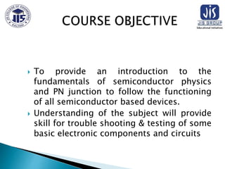
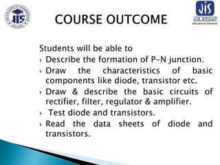
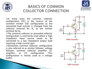
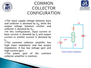
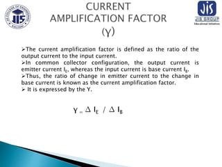
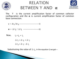
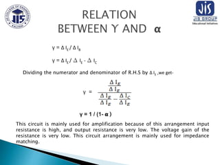
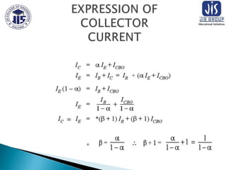
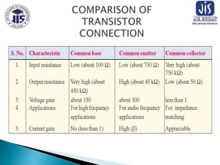
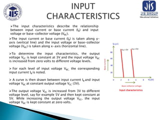
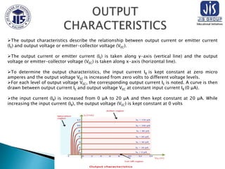
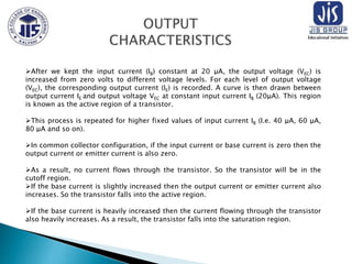
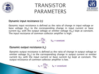
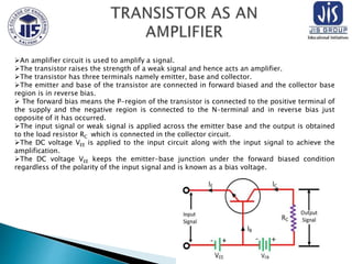
PRESENTED BY-
GARGI ROY
ASSISTANT PROFESSOR
ELECTRICAL ENGINEERING DEPARTMENT
JIS COLLEGE OF ENGINEERING
SUBJECT CODE - EE/S3/BE(for Diploma)
CREDIT-4
 To provide an introduction to the
fundamentals of semiconductor physics
and PN junction to follow the functioning
of all semiconductor based devices.
 Understanding of the subject will provide
skill for trouble shooting & testing of some
basic electronic components and circuits
Students will be able to
 Describe the formation of P-N junction.
 Draw the characteristics of basic
components like diode, transistor etc.
 Draw & describe the basic circuits of
rectifier, filter, regulator & amplifier.
 Test diode and transistors.
 Read the data sheets of diode and
transistors.
TRANSISTOR
CONNECTION
(COMMON
COLLECTOR )
The Common Collector connection is another type of bipolar
junction transistor, (BJT) configuration, where the input signal is
applied to the base terminal and the output signal taken from the
emitter terminal.
Thus the collector terminal is common to both the input and output
circuits.
This type of configuration is called Common Collector, (CC)
because the collector terminal is effectively “grounded” or “earthed”
through the power supply.
In many ways the common collector
configuration (CC) is the reverse of the
common emitter (CE) configuration as the
connected load resistor is changed from the
collector terminal for RC to the emitter
terminal for RE.
The common collector or grounded collector
configuration is commonly used where a high
impedance input source needs to be
connected to a low impedance output load
requiring a high current gain
Sometimes common collector configuration
is also referred to as emitter follower, voltage
follower, common collector amplifier, CC
amplifier, or CC configuration. This
configuration is mostly used as a voltage
buffer.
The input supply voltage between base
and collector is denoted by VBC while the
output voltage between emitter and
collector is denoted by VEC.
In this configuration, input current or
base current is denoted by IB and output
current or emitter current is denoted by
IE.
The common collector amplifier has
high input impedance and low output
impedance. It has low voltage gain and
high current gain.
The power gain of the common
collector amplifier is medium.
The current amplification factor is defined as the ratio of the
output current to the input current.
In common collector configuration, the output current is
emitter current IE, whereas the input current is base current IB.
Thus, the ratio of change in emitter current to the change in
base current is known as the current amplification factor.
 It is expressed by the Y.
γ = ∆ IE / ∆ IB
The Υ is the current amplification factor of common collector
configuration and the α is current amplification factor of common
base connection.
γ = ∆ IE / ∆ IB ---------------------------------i)
𝝰 = ∆ IC / ∆ IE --------------------------ii)
IE = IB + IC
∆ IE = ∆ IB + ∆ IC
∆ IB = ∆ IE - ∆ IC
Now,
Substituting the value of ∆ IB in the equation i) we get---
γ = ∆ IE / ∆ IB
γ = ∆ IE / ∆ IE - ∆ IC
Dividing the numerator and denominator of R.H.S by ∆ IE ,we get-
γ =
γ = 1 / (1- 𝝰 )
This circuit is mainly used for amplification because of this arrangement input
resistance is high, and output resistance is very low. The voltage gain of the
resistance is very low. This circuit arrangement is mainly used for impedance
matching.
The input characteristics describe the relationship
between input current or base current (IB) and input
voltage or base-collector voltage (VBC).
The input current or base current (IB) is taken along y-
axis (vertical line) and the input voltage or base-collector
voltage (VBC) is taken along x-axis (horizontal line).
To determine the input characteristics, the output
voltage VEC is kept constant at 3V and the input voltage VBC
is increased from zero volts to different voltage levels.
 For each level of input voltage VBC, the corresponding
input current IB is noted.
 A curve is then drawn between input current IB and input
voltage VBC at constant output voltage VEC (3V).
The output voltage VEC is increased from 3V to different
voltage level, say for example 5V and then kept constant at
5V. While increasing the output voltage VEC, the input
voltage VBC is kept constant at zero volts.
The output characteristics describe the relationship between output current or emitter current
(IE) and output voltage or emitter-collector voltage (VEC).
The output current or emitter current (IE) is taken along y-axis (vertical line) and the output
voltage or emitter-collector voltage (VEC) is taken along x-axis (horizontal line).
To determine the output characteristics, the input current IB is kept constant at zero micro
amperes and the output voltage VEC is increased from zero volts to different voltage levels.
For each level of output voltage VEC, the corresponding output current IE is noted. A curve is then
drawn between output current IE and output voltage VEC at constant input current IB (0 μA).
the input current (IB) is increased from 0 μA to 20 μA and then kept constant at 20 μA. While
increasing the input current (IB), the output voltage (VEC) is kept constant at 0 volts
After we kept the input current (IB) constant at 20 μA, the output voltage (VEC) is
increased from zero volts to different voltage levels. For each level of output voltage
(VEC), the corresponding output current (IE) is recorded. A curve is then drawn between
output current IE and output voltage VEC at constant input current IB (20μA). This region
is known as the active region of a transistor.
This process is repeated for higher fixed values of input current IB (I.e. 40 μA, 60 μA,
80 μA and so on).
In common collector configuration, if the input current or base current is zero then the
output current or emitter current is also zero.
As a result, no current flows through the transistor. So the transistor will be in the
cutoff region.
If the base current is slightly increased then the output current or emitter current also
increases. So the transistor falls into the active region.
If the base current is heavily increased then the current flowing through the transistor
also heavily increases. As a result, the transistor falls into the saturation region.
Dynamic input resistance (ri)
Dynamic input resistance is defined as the ratio of change in input voltage or
base voltage (VBC) to the corresponding change in input current or base
current (IB), with the output voltage or emitter voltage (VEC) kept at constant.
The input resistance of common collector amplifier is high.
Dynamic output resistance (ro)
Dynamic output resistance is defined as the ratio of change in output voltage or
emitter voltage (VEC) to the corresponding change in output current or emitter
current (IE), with the input current or base current (IB) kept at constant. The
output resistance of common collector amplifier is low.
An amplifier circuit is used to amplify a signal.
The transistor raises the strength of a weak signal and hence acts an amplifier.
The transistor has three terminals namely emitter, base and collector.
The emitter and base of the transistor are connected in forward biased and the collector base
region is in reverse bias.
 The forward bias means the P-region of the transistor is connected to the positive terminal of
the supply and the negative region is connected to the N-terminal and in reverse bias just
opposite of it has occurred.
The input signal or weak signal is applied across the emitter base and the output is obtained
to the load resistor RC which is connected in the collector circuit.
The DC voltage VEE is applied to the input circuit along with the input signal to achieve the
amplification.
The DC voltage VEE keeps the emitter-base junction under the forward biased condition
regardless of the polarity of the input signal and is known as a bias voltage.
When a weak signal is applied to the input, a small change in signal
voltage causes a change in emitter current (or we can say a change of
0.1V in signal voltage causes a change of 1mA in the emitter current)
because the input circuit has very low resistance.
This change is almost the same in collector current because of the
transmitter action.
In the collector circuit, a load resistor RC of high value is connected.
When collector current flows through such a high resistance, it
produces a large voltage drop across it.
Thus, a weak signal (0.1V) applied to the input circuit appears in the
amplified form (10V) in the collector circuit.
 Introduction
 Common collector transistor
Common collector configuration
Current amplification factor
Relation between current amplification for CC mode &
current amplification factor for CB mode
Expression of collector current
Input Characteristics
Output Characteristics
Transistor parameters
Transistor as an amplifier
 What is CC configuration?
 What are the applications of CC mode of
transistor?
 What are the input and output characteristics
of CC mode transistor?
 https://www.instructables.com/
 https://circuitglobe.com/
 https://www.electrical4u.com/npn-
transistor/
 https://www.electronics-notes.com/
CC MODE engerring basic electrical skdkf

CC MODE engerring basic electrical skdkf

  • 1.
    PRESENTED BY- GARGI ROY ASSISTANTPROFESSOR ELECTRICAL ENGINEERING DEPARTMENT JIS COLLEGE OF ENGINEERING
  • 2.
    SUBJECT CODE -EE/S3/BE(for Diploma) CREDIT-4
  • 3.
     To providean introduction to the fundamentals of semiconductor physics and PN junction to follow the functioning of all semiconductor based devices.  Understanding of the subject will provide skill for trouble shooting & testing of some basic electronic components and circuits
  • 4.
    Students will beable to  Describe the formation of P-N junction.  Draw the characteristics of basic components like diode, transistor etc.  Draw & describe the basic circuits of rectifier, filter, regulator & amplifier.  Test diode and transistors.  Read the data sheets of diode and transistors.
  • 5.
  • 6.
    The Common Collectorconnection is another type of bipolar junction transistor, (BJT) configuration, where the input signal is applied to the base terminal and the output signal taken from the emitter terminal. Thus the collector terminal is common to both the input and output circuits. This type of configuration is called Common Collector, (CC) because the collector terminal is effectively “grounded” or “earthed” through the power supply.
  • 7.
    In many waysthe common collector configuration (CC) is the reverse of the common emitter (CE) configuration as the connected load resistor is changed from the collector terminal for RC to the emitter terminal for RE. The common collector or grounded collector configuration is commonly used where a high impedance input source needs to be connected to a low impedance output load requiring a high current gain Sometimes common collector configuration is also referred to as emitter follower, voltage follower, common collector amplifier, CC amplifier, or CC configuration. This configuration is mostly used as a voltage buffer.
  • 8.
    The input supplyvoltage between base and collector is denoted by VBC while the output voltage between emitter and collector is denoted by VEC. In this configuration, input current or base current is denoted by IB and output current or emitter current is denoted by IE. The common collector amplifier has high input impedance and low output impedance. It has low voltage gain and high current gain. The power gain of the common collector amplifier is medium.
  • 9.
    The current amplificationfactor is defined as the ratio of the output current to the input current. In common collector configuration, the output current is emitter current IE, whereas the input current is base current IB. Thus, the ratio of change in emitter current to the change in base current is known as the current amplification factor.  It is expressed by the Y. γ = ∆ IE / ∆ IB
  • 10.
    The Υ isthe current amplification factor of common collector configuration and the α is current amplification factor of common base connection. γ = ∆ IE / ∆ IB ---------------------------------i) 𝝰 = ∆ IC / ∆ IE --------------------------ii) IE = IB + IC ∆ IE = ∆ IB + ∆ IC ∆ IB = ∆ IE - ∆ IC Now, Substituting the value of ∆ IB in the equation i) we get---
  • 11.
    γ = ∆IE / ∆ IB γ = ∆ IE / ∆ IE - ∆ IC Dividing the numerator and denominator of R.H.S by ∆ IE ,we get- γ = γ = 1 / (1- 𝝰 ) This circuit is mainly used for amplification because of this arrangement input resistance is high, and output resistance is very low. The voltage gain of the resistance is very low. This circuit arrangement is mainly used for impedance matching.
  • 14.
    The input characteristicsdescribe the relationship between input current or base current (IB) and input voltage or base-collector voltage (VBC). The input current or base current (IB) is taken along y- axis (vertical line) and the input voltage or base-collector voltage (VBC) is taken along x-axis (horizontal line). To determine the input characteristics, the output voltage VEC is kept constant at 3V and the input voltage VBC is increased from zero volts to different voltage levels.  For each level of input voltage VBC, the corresponding input current IB is noted.  A curve is then drawn between input current IB and input voltage VBC at constant output voltage VEC (3V). The output voltage VEC is increased from 3V to different voltage level, say for example 5V and then kept constant at 5V. While increasing the output voltage VEC, the input voltage VBC is kept constant at zero volts.
  • 15.
    The output characteristicsdescribe the relationship between output current or emitter current (IE) and output voltage or emitter-collector voltage (VEC). The output current or emitter current (IE) is taken along y-axis (vertical line) and the output voltage or emitter-collector voltage (VEC) is taken along x-axis (horizontal line). To determine the output characteristics, the input current IB is kept constant at zero micro amperes and the output voltage VEC is increased from zero volts to different voltage levels. For each level of output voltage VEC, the corresponding output current IE is noted. A curve is then drawn between output current IE and output voltage VEC at constant input current IB (0 μA). the input current (IB) is increased from 0 μA to 20 μA and then kept constant at 20 μA. While increasing the input current (IB), the output voltage (VEC) is kept constant at 0 volts
  • 16.
    After we keptthe input current (IB) constant at 20 μA, the output voltage (VEC) is increased from zero volts to different voltage levels. For each level of output voltage (VEC), the corresponding output current (IE) is recorded. A curve is then drawn between output current IE and output voltage VEC at constant input current IB (20μA). This region is known as the active region of a transistor. This process is repeated for higher fixed values of input current IB (I.e. 40 μA, 60 μA, 80 μA and so on). In common collector configuration, if the input current or base current is zero then the output current or emitter current is also zero. As a result, no current flows through the transistor. So the transistor will be in the cutoff region. If the base current is slightly increased then the output current or emitter current also increases. So the transistor falls into the active region. If the base current is heavily increased then the current flowing through the transistor also heavily increases. As a result, the transistor falls into the saturation region.
  • 17.
    Dynamic input resistance(ri) Dynamic input resistance is defined as the ratio of change in input voltage or base voltage (VBC) to the corresponding change in input current or base current (IB), with the output voltage or emitter voltage (VEC) kept at constant. The input resistance of common collector amplifier is high. Dynamic output resistance (ro) Dynamic output resistance is defined as the ratio of change in output voltage or emitter voltage (VEC) to the corresponding change in output current or emitter current (IE), with the input current or base current (IB) kept at constant. The output resistance of common collector amplifier is low.
  • 18.
    An amplifier circuitis used to amplify a signal. The transistor raises the strength of a weak signal and hence acts an amplifier. The transistor has three terminals namely emitter, base and collector. The emitter and base of the transistor are connected in forward biased and the collector base region is in reverse bias.  The forward bias means the P-region of the transistor is connected to the positive terminal of the supply and the negative region is connected to the N-terminal and in reverse bias just opposite of it has occurred. The input signal or weak signal is applied across the emitter base and the output is obtained to the load resistor RC which is connected in the collector circuit. The DC voltage VEE is applied to the input circuit along with the input signal to achieve the amplification. The DC voltage VEE keeps the emitter-base junction under the forward biased condition regardless of the polarity of the input signal and is known as a bias voltage.
  • 19.
    When a weaksignal is applied to the input, a small change in signal voltage causes a change in emitter current (or we can say a change of 0.1V in signal voltage causes a change of 1mA in the emitter current) because the input circuit has very low resistance. This change is almost the same in collector current because of the transmitter action. In the collector circuit, a load resistor RC of high value is connected. When collector current flows through such a high resistance, it produces a large voltage drop across it. Thus, a weak signal (0.1V) applied to the input circuit appears in the amplified form (10V) in the collector circuit.
  • 20.
     Introduction  Commoncollector transistor Common collector configuration Current amplification factor Relation between current amplification for CC mode & current amplification factor for CB mode Expression of collector current Input Characteristics Output Characteristics Transistor parameters Transistor as an amplifier
  • 21.
     What isCC configuration?  What are the applications of CC mode of transistor?  What are the input and output characteristics of CC mode transistor?
  • 22.
     https://www.instructables.com/  https://circuitglobe.com/ https://www.electrical4u.com/npn- transistor/  https://www.electronics-notes.com/