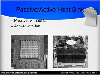
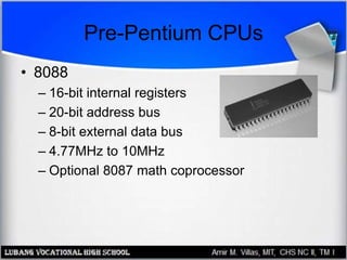
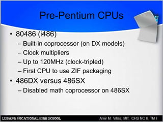
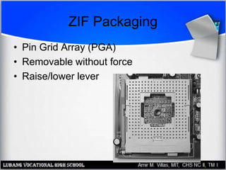
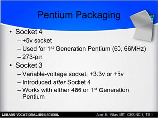
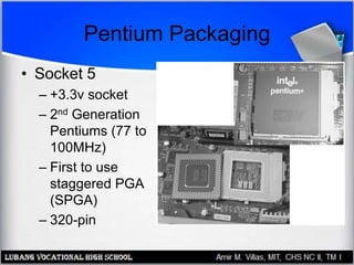
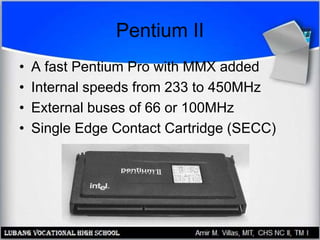
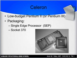
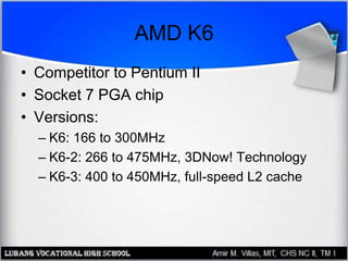
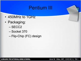
PC Hardware Servicing
Chapter 5: CPUs
Chapter 5 Objectives
• Understand how a CPU holds and
processes data
• Identify ways by which a CPU is
categorized and evaluated
• Distinguish between PGA and SECC
packaging
• Understand how modern CPUs have
evolved from earlier versions
Inside the CPU
• Low-order bits: data that represents
numbers to be calculated
• High-order bits: data that represents
instructions to the CPU
Inside the CPU
• Instruction set: high-order bit codes that
the CPU understands
• Registers: holding areas for data inside
the CPU
Example Process
Data Processing Speed
• External speed
– Speed at which motherboard and CPU
communicate
– Controlled by system crystal
• Internal speed
– Speed at which CPU performs internal
operations
– Usually a multiple of the external speed
Overclocking and Underclocking
• Overclocking: operating a CPU at a
higher internal speed than it is rated for
• Underclocking: operating a CPU at a
lower internal speed than it is rated for
Core Voltage
• Voltage that the CPU requires to operate
• Ranges from approximately +1.5v to +5v
• Newer CPUs = lower voltages
• Motherboard must provide correct voltage
CPU Cache Usage
• L1 cache
– Front-side cache
– Holds data waiting to enter the CPU
– Built into the CPU on modern systems
• L2 cache
– Back-side cache
– Holds data exiting the CPU
– Built into the CPU packaging, but on a
separate chip
CPU Cooling
• Fan
– Pulls heat away from CPU
• Heat sink
– Spikes channel heat away from CPU
Passive/Active Heat Sink
– Passive: without fan
– Active: with fan
Pre-Pentium CPUs
• 8088
– 16-bit internal registers
– 20-bit address bus
– 8-bit external data bus
– 4.77MHz to 10MHz
– Optional 8087 math coprocessor
Pre-Pentium CPUs
• 80286
– Could run in Protected Mode
• More RAM could be addressed
• Multitasking
– Could run in Real Mode
• Backward compatible with applications for 8088
– Could use expanded memory on an ISA
expansion board
– Up to 20MHz in speed
Pre-Pentium CPUs
• 80386 (i386)
– 386 protected mode, 286 protected mode,
and real mode
– Virtual memory
– Virtual 8086 mode
• 386DX versus 386SX
– 32-bit versus 16-bit external data bus
– 32-bit versus 24-bit address bus
Pre-Pentium CPUs
• 80486 (i486)
– Built-in coprocessor (on DX models)
– Clock multipliers
– Up to 120MHz (clock-tripled)
– First CPU to use ZIF packaging
• 486DX versus 486SX
– Disabled math coprocessor on 486SX
ZIF Packaging
• Pin Grid Array (PGA)
• Removable without force
• Raise/lower lever
Pentium Packaging
• Socket 4
– +5v socket
– Used for 1st Generation Pentium (60, 66MHz)
– 273-pin
• Socket 3
– Variable-voltage socket, +3.3v or +5v
– Introduced after Socket 4
– Works with either 486 or 1st Generation
Pentium
Pentium Packaging
• Socket 5
– +3.3v socket
– 2nd Generation
Pentiums (77 to
100MHz)
– First to use
staggered PGA
(SPGA)
– 320-pin
Pentium Packaging
• Socket 6
– +3.3v socket
– Used for Pentium OverDrive and 486DX4
• Socket 7
– Variable voltage socket, +3.3v or +5v
– 321 pins (rather than 320 on Socket 5)
– Otherwise the same as Socket 5
Pentium Packaging
• Super Socket 7 (Super7)
– Enhanced Socket 7
– Used with 2nd Generation Pentium and non-Intel
competitor chips
– Provides split voltage capability that allows higher
external than internal voltage
Pentium CPUs
• First-Generation
– 60 or 66MHz
– Used Socket 3 or Socket 4
• Second-Generation
– 75 to 100MHz
– Used Socket 5 or Socket 7
• Third-Generation
– 166 to 233MHz
– Adds MMX capability
Pentium Pro
• Improvement on Second-Generation
Pentium
• Introduced quad pipelining
• Introduced on-chip L2 cache
• Lacked MMX
• Optimized for 32-bit operating systems
• Socket 8: +3v rectangular socket, 387 pins
Pentium II
• A fast Pentium Pro with MMX added
• Internal speeds from 233 to 450MHz
• External buses of 66 or 100MHz
• Single Edge Contact Cartridge (SECC)
Celeron
• Low-budget Pentium II (or Pentium III)
• Packaging:
– Single Edge Processor (SEP)
– Socket 370
AMD K6
• Competitor to Pentium II
• Socket 7 PGA chip
• Versions:
– K6: 166 to 300MHz
– K6-2: 266 to 475MHz, 3DNow! Technology
– K6-3: 400 to 450MHz, full-speed L2 cache
Pentium III
• 450MHz to 1GHz
• Packaging:
– SECC2
– Socket 370
– Flip-Chip (FC) design
Pentium 4
• 1.3GHz to more than 2.8GHz
• Socket 423 or Socket 478
• NetBurst architecture
• 64-bit, 100MHz quad pipelining
• 20Kb L1 cache, 256KB full-speed L2
cache

CPUs

  • 1.
  • 2.
    Chapter 5 Objectives •Understand how a CPU holds and processes data • Identify ways by which a CPU is categorized and evaluated • Distinguish between PGA and SECC packaging • Understand how modern CPUs have evolved from earlier versions
  • 3.
    Inside the CPU •Low-order bits: data that represents numbers to be calculated • High-order bits: data that represents instructions to the CPU
  • 4.
    Inside the CPU •Instruction set: high-order bit codes that the CPU understands • Registers: holding areas for data inside the CPU
  • 5.
  • 6.
    Data Processing Speed •External speed – Speed at which motherboard and CPU communicate – Controlled by system crystal • Internal speed – Speed at which CPU performs internal operations – Usually a multiple of the external speed
  • 7.
    Overclocking and Underclocking •Overclocking: operating a CPU at a higher internal speed than it is rated for • Underclocking: operating a CPU at a lower internal speed than it is rated for
  • 8.
    Core Voltage • Voltagethat the CPU requires to operate • Ranges from approximately +1.5v to +5v • Newer CPUs = lower voltages • Motherboard must provide correct voltage
  • 9.
    CPU Cache Usage •L1 cache – Front-side cache – Holds data waiting to enter the CPU – Built into the CPU on modern systems • L2 cache – Back-side cache – Holds data exiting the CPU – Built into the CPU packaging, but on a separate chip
  • 10.
    CPU Cooling • Fan –Pulls heat away from CPU • Heat sink – Spikes channel heat away from CPU
  • 11.
    Passive/Active Heat Sink –Passive: without fan – Active: with fan
  • 12.
    Pre-Pentium CPUs • 8088 –16-bit internal registers – 20-bit address bus – 8-bit external data bus – 4.77MHz to 10MHz – Optional 8087 math coprocessor
  • 13.
    Pre-Pentium CPUs • 80286 –Could run in Protected Mode • More RAM could be addressed • Multitasking – Could run in Real Mode • Backward compatible with applications for 8088 – Could use expanded memory on an ISA expansion board – Up to 20MHz in speed
  • 14.
    Pre-Pentium CPUs • 80386(i386) – 386 protected mode, 286 protected mode, and real mode – Virtual memory – Virtual 8086 mode • 386DX versus 386SX – 32-bit versus 16-bit external data bus – 32-bit versus 24-bit address bus
  • 15.
    Pre-Pentium CPUs • 80486(i486) – Built-in coprocessor (on DX models) – Clock multipliers – Up to 120MHz (clock-tripled) – First CPU to use ZIF packaging • 486DX versus 486SX – Disabled math coprocessor on 486SX
  • 16.
    ZIF Packaging • PinGrid Array (PGA) • Removable without force • Raise/lower lever
  • 17.
    Pentium Packaging • Socket4 – +5v socket – Used for 1st Generation Pentium (60, 66MHz) – 273-pin • Socket 3 – Variable-voltage socket, +3.3v or +5v – Introduced after Socket 4 – Works with either 486 or 1st Generation Pentium
  • 18.
    Pentium Packaging • Socket5 – +3.3v socket – 2nd Generation Pentiums (77 to 100MHz) – First to use staggered PGA (SPGA) – 320-pin
  • 19.
    Pentium Packaging • Socket6 – +3.3v socket – Used for Pentium OverDrive and 486DX4 • Socket 7 – Variable voltage socket, +3.3v or +5v – 321 pins (rather than 320 on Socket 5) – Otherwise the same as Socket 5
  • 20.
    Pentium Packaging • SuperSocket 7 (Super7) – Enhanced Socket 7 – Used with 2nd Generation Pentium and non-Intel competitor chips – Provides split voltage capability that allows higher external than internal voltage
  • 21.
    Pentium CPUs • First-Generation –60 or 66MHz – Used Socket 3 or Socket 4 • Second-Generation – 75 to 100MHz – Used Socket 5 or Socket 7 • Third-Generation – 166 to 233MHz – Adds MMX capability
  • 22.
    Pentium Pro • Improvementon Second-Generation Pentium • Introduced quad pipelining • Introduced on-chip L2 cache • Lacked MMX • Optimized for 32-bit operating systems • Socket 8: +3v rectangular socket, 387 pins
  • 23.
    Pentium II • Afast Pentium Pro with MMX added • Internal speeds from 233 to 450MHz • External buses of 66 or 100MHz • Single Edge Contact Cartridge (SECC)
  • 24.
    Celeron • Low-budget PentiumII (or Pentium III) • Packaging: – Single Edge Processor (SEP) – Socket 370
  • 25.
    AMD K6 • Competitorto Pentium II • Socket 7 PGA chip • Versions: – K6: 166 to 300MHz – K6-2: 266 to 475MHz, 3DNow! Technology – K6-3: 400 to 450MHz, full-speed L2 cache
  • 26.
    Pentium III • 450MHzto 1GHz • Packaging: – SECC2 – Socket 370 – Flip-Chip (FC) design
  • 27.
    Pentium 4 • 1.3GHzto more than 2.8GHz • Socket 423 or Socket 478 • NetBurst architecture • 64-bit, 100MHz quad pipelining • 20Kb L1 cache, 256KB full-speed L2 cache