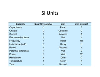
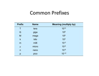
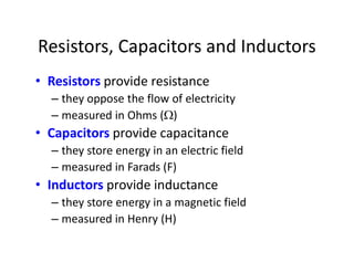
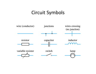
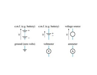
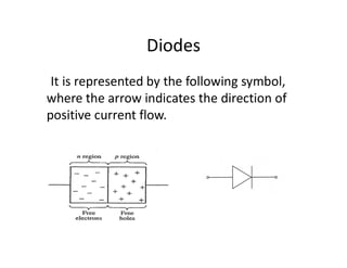
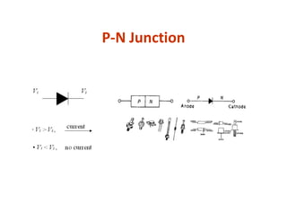
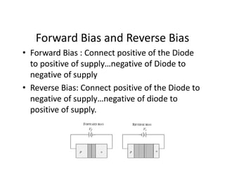
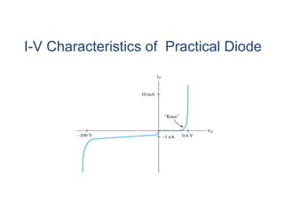
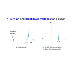
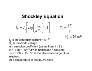
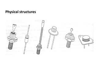
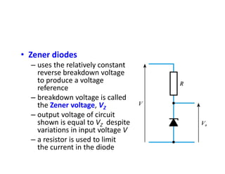
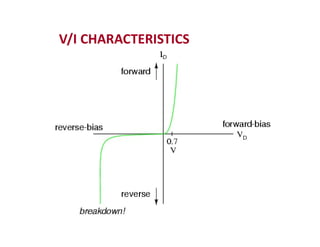
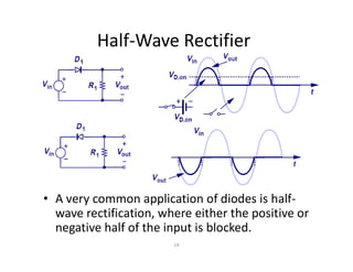
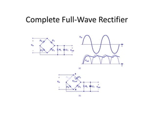
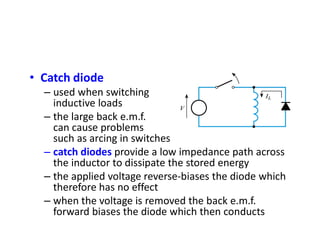
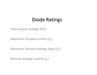
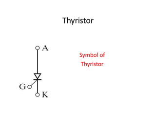
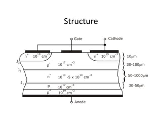
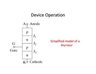
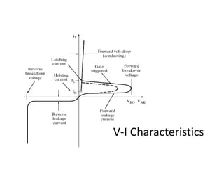
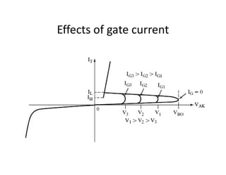
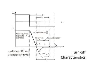
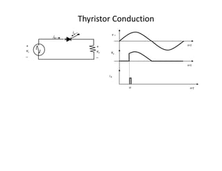
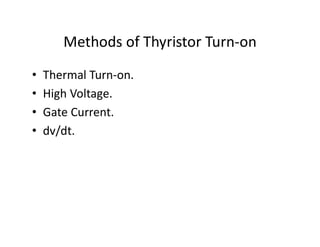
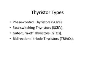
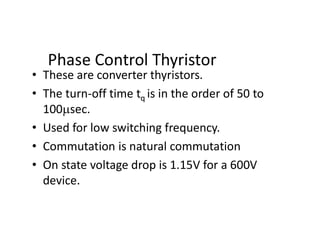
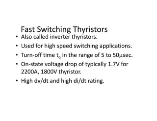
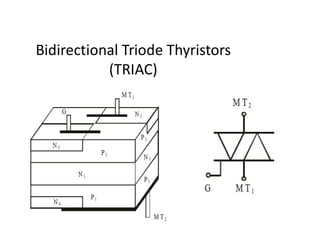
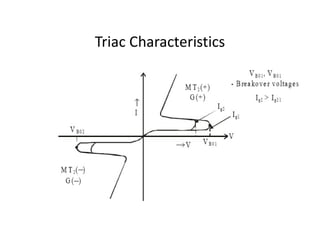
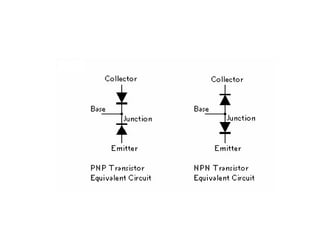
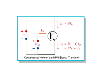
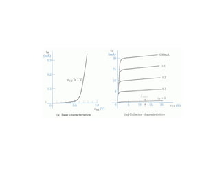
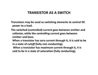
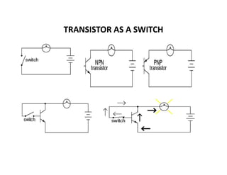
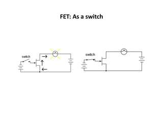
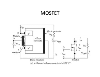
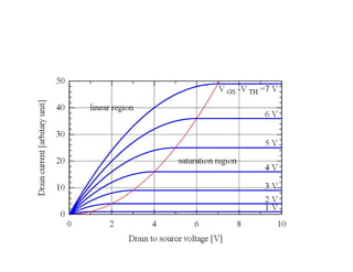
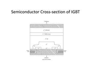
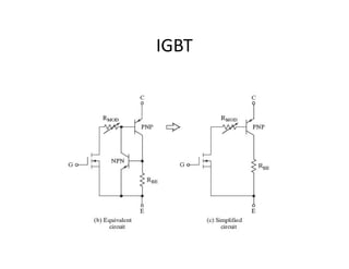
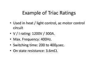
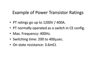
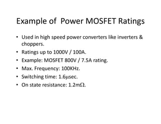
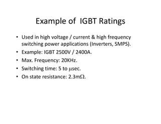
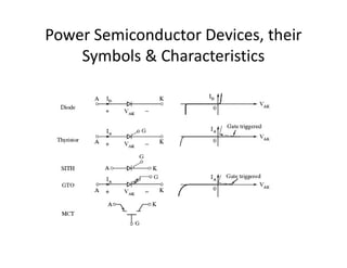
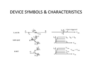
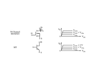
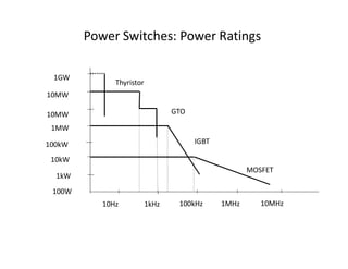
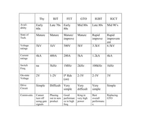
Basic Power Electronics
Components
SI Units
Quantity Quantity symbol Unit Unit symbol
Capacitance C Farad F
Charge Q Coulomb C
Current I Ampere A
Electromotive force E Volt V
Frequency f Hertz Hz
Inductance (self) L Henry H
Period T Second s
Potential difference V Volt V
Power P Watt W
Resistance R Ohm Ω
Temperature T Kelvin K
Time t Second s
Common Prefixes
Prefix Name Meaning (multiply by)
T tera 1012
G giga 109
M mega 106
k kilo 103
m milli 10-3
 micro 10-6
n nano 10-9
p pico 10-12
Resistors, Capacitors and Inductors
• Resistors provide resistance
– they oppose the flow of electricity
– measured in Ohms ()
• Capacitors provide capacitance
– they store energy in an electric field
– measured in Farads (F)
• Inductors provide inductance
– they store energy in a magnetic field
– measured in Henry (H)
Circuit Symbols
Diodes
It is represented by the following symbol,
where the arrow indicates the direction of
positive current flow.
P-N Junction
Forward Bias and Reverse Bias
• Forward Bias : Connect positive of the Diode
to positive of supply…negative of Diode to
negative of supply
• Reverse Bias: Connect positive of the Diode to
negative of supply…negative of diode to
positive of supply.
I-V Characteristics of Practical Diode
• Turn-on and breakdown voltages for a silicon
device
Shockley Equation















 1
exp
T
D
s
D
nV
v
I
i
q
kT
VT 
Is is the saturation current ~10 -14
Vd is the diode voltage
n – emission coefficient (varies from 1 - 2 )
k = 1.38 × 10⁻²³ J/K is Boltzmann’s constant
q = 1.60 × 10⁻¹⁹ C is the electrical charge of an
electron.
At a temperature of 300 K, we have
mV
26

T
V
Physical structures
• Silicon diodes
– generally have a turn-on voltage of about 0.5 V
– generally have a conduction voltage of about 0.7 V
– have a breakdown voltage that depends on their
construction
• perhaps 75 V for a small-signal diode
• perhaps 400 V for a power device
– have a maximum current that depends on their
construction
• perhaps 100 mA for a small-signal diode
• perhaps many amps for a power device
• Schottky diodes
– formed by the junction between a layer of metal
(e.g. aluminium) and a semiconductor
– action relies only on majority charge carriers
– much faster in operation than a pn junction diode
– has a low forward voltage drop of about 0.25 V
– used in the design of high-speed logic gates
Zener diodes
• A Zener diode is a pn silicon junction diode that is
reverse biased and with the supply voltage sufficient
to produce the ‘avalanche’ or ‘breakdown’ effect.
• A zener diode must be used in conjunction with a
‘current-limiting’ resistor to keep the current flow
through the diode to a safe level.
• A zener diode is used to produce a stable voltage
from a supply which is fluctuating.
• Zener diodes
– uses the relatively constant
reverse breakdown voltage
to produce a voltage
reference
– breakdown voltage is called
the Zener voltage, VZ
– output voltage of circuit
shown is equal to VZ despite
variations in input voltage V
– a resistor is used to limit
the current in the diode
V/I CHARACTERISTICS
19
Half-Wave Rectifier
• A very common application of diodes is half-
wave rectification, where either the positive or
negative half of the input is blocked.
Complete Full-Wave Rectifier
• Catch diode
– used when switching
inductive loads
– the large back e.m.f.
can cause problems
such as arcing in switches
– catch diodes provide a low impedance path across
the inductor to dissipate the stored energy
– the applied voltage reverse-biases the diode which
therefore has no effect
– when the voltage is removed the back e.m.f.
forward biases the diode which then conducts
Diode Ratings
Peak inverse voltage (PIV)
Maximum forward current (IF)
Maximum forward voltage drop (VF)
Reverse leakage current (IR)
Diode handling and installation
Diodes are polarized and must be installed in with correct
orientation.
Many diodes are modestly susceptible to ESD damage, so
normal ESD precautions should be taken.
Mechanical stress due to lead bending should be
minimized.
Thyristor
Symbol of
Thyristor
Thyristors
• Most important type of power semiconductor
device.
• Have the highest power handling
capability.they have a rating of 5000V / 6000A
with switching frequencies ranging from 1KHz
to 20KHz.
• Is inherently a slow switching device
compared to BJT or MOSFET.
• Used as a latching switch that can be turned
on by the control terminal but cannot be
turned off by the gate.
Structure




Gate Cathode
J3
J2
J1
Anode
10 cm
17 -3
10 -5 x 10 cm
13 14 -3
10 cm
17 -3
10 cm
19 -3
10 cm
19 -3
10 cm
19 -3
n
+
n
+
p
-
n
–
p
p
+
10 m

30-100 m

50-1000 m

30-50 m

Device Operation
Simplified model of a
thyristor
V-I Characteristics
Effects of gate current
Turn-off
Characteristics
Anode current
begins to
decrease
tC
tq
t
t
Commutation
di
dt
Recovery Recombination
t1
t2 t3 t4 t5
trr tgr
tq
tc
VAK
IA
tq=device off time
tc=circuit off time
Thyristor Conduction
+
vo
_
+
vs
_
ig
ia
w t
vo
a
i g
w t
w t
v s
Methods of Thyristor Turn-on
• Thermal Turn-on.
• High Voltage.
• Gate Current.
• dv/dt.
Thyristor Types
• Phase-control Thyristors (SCR’s).
• Fast-switching Thyristors (SCR’s).
• Gate-turn-off Thyristors (GTOs).
• Bidirectional triode Thyristors (TRIACs).
Phase Control Thyristor
• These are converter thyristors.
• The turn-off time tq is in the order of 50 to
100sec.
• Used for low switching frequency.
• Commutation is natural commutation
• On state voltage drop is 1.15V for a 600V
device.
Fast Switching Thyristors
• Also called inverter thyristors.
• Used for high speed switching applications.
• Turn-off time tq in the range of 5 to 50sec.
• On-state voltage drop of typically 1.7V for
2200A, 1800V thyristor.
• High dv/dt and high di/dt rating.
Bidirectional Triode Thyristors
(TRIAC)
Triac Characteristics
Gate Turn-off Thyristors
• Turned on by applying positive gate signal.
• Turned off by applying negative gate signal.
• On state voltage is 3.4V for 550A, 1200V GTO.
• Controllable peak on-state current ITGQ is the
peak value of on-state current which can be
turned-off by gate control.
Advantages over SCRs
• Elimination of commutating components.
• Reduction in acoustic & electromagnetic noise
due to elimination of chokes.
• Faster turn-off, therefore can be used for
higher switching frequencies.
• Improved efficiency of converters.
Advantages over BJTs
• Higher voltage blocking capabilities.
• High on-state gain.
• High ratio of peak surge current to average
current.
• A pulsed gate signal of short duration only is
required.
Disadvantages of GTOs
• On-state voltage drop is more.
• Due to multi cathode structure higher gate
current is required.
• Gate drive circuit losses are more.
• Reverse blocking capability is less than its
forward blocking capability.
Bipolar Transistor
TRANSISTOR AS A SWITCH
Transistors may be used as switching elements to control DC
power to a load.
The switched (controlled) current goes between emitter and
collector, while the controlling current goes between
emitter and base.
When a transistor has zero current through it, it is said to be
in a state of cutoff (fully non conducting).
When a transistor has maximum current through it, it is
said to be in a state of saturation (fully conducting).
TRANSISTOR AS A SWITCH
TRANSISTOR AS AN AMPLIFIER
Field Effect Transistor (FET)
FET: N-Channel
FET: P-Channel
FET: As a switch
MOSFET
Semiconductor Cross-section of IGBT
IGBT
Advantages of IGBT
• Combines the advantages of BJT & MOSFET
• High input impedance like MOSFET
• Voltage controlled device like MOSFET
• Simple gate drive, Lower switching loss
• Low on state conduction power loss like BJT
• Higher current capability & higher switching speed
than a BJT. ( Switching speed lower than MOSFET)
Applications of IGBT
• ac and dc motor controls.
• General purpose inverters.
• Uninterrupted Power Supply (UPS).
• Welding Equipments.
• Numerical control, Cutting tools.
• Robotics & Induction heating.
Example of Inverter Grade Thyristor
Ratings
• V / I rating: 4500V / 3000A.
• Max. Frequency: 20KHz.
• Switching time: 20 to 100sec.
• On state resistance: 0.5m.
Example of Triac Ratings
• Used in heat / light control, ac motor control
circuit
• V / I rating: 1200V / 300A.
• Max. Frequency: 400Hz.
• Switching time: 200 to 400sec.
• On state resistance: 3.6m.
Example of Power Transistor Ratings
• PT ratings go up to 1200V / 400A.
• PT normally operated as a switch in CE config.
• Max. Frequency: 400Hz.
• Switching time: 200 to 400sec.
• On state resistance: 3.6m.
Example of Power MOSFET Ratings
• Used in high speed power converters like inverters &
choppers.
• Ratings up to 1000V / 100A.
• Example: MOSFET 800V / 7.5A rating.
• Max. Frequency: 100KHz.
• Switching time: 1.6sec.
• On state resistance: 1.2m.
Example of IGBT Ratings
• Used in high voltage / current & high frequency
switching power applications (Inverters, SMPS).
• Example: IGBT 2500V / 2400A.
• Max. Frequency: 20KHz.
• Switching time: 5 to sec.
• On state resistance: 2.3m.
Designing – Heat Sinking
Power Semiconductor Devices, their
Symbols & Characteristics
DEVICE SYMBOLS & CHARACTERISTICS
Power Switches: Power Ratings
10Hz 1kHz 1MHz
100kHz 10MHz
1kW
100kW
10kW
10MW
1MW
10MW
1GW
100W
MOSFET
IGBT
GTO
Thyristor
Thy BJT FET GTO IGBT IGCT
Avail-
abilty
Early
60s
Late 70s Early
80s
Mid 80s Late 80s Mid 90’s
State of
Tech.
Mature Mature Mature/
improve
Mature Rapid
improve
Rapid
improvem
ent
Voltage
ratings
5kV 1kV 500V 5kV 3.3kV 6.5kV
Current
ratings
4kA 400A 200A 5kA 1.2kA 4kA
Switch
Freq.
na 5kHz 1MHz 2kHz 100kHz 1kHz
On-state
Voltage
2V 1-2V I* Rds
(on)
2-3V 2-3V 3V
Drive
Circuit
Simple Difficult Very
simple
Very
difficult
Very
simple
Simple
Comm-ents Cannot
turn off
using gate
signals
Phasing
out in new
product
Good
performan
ce in high
freq.
King in
very high
power
Best
overall
performanc
e.
Replacing
GTO

Basic Power Electronics Components Lists

  • 1.
  • 2.
    SI Units Quantity Quantitysymbol Unit Unit symbol Capacitance C Farad F Charge Q Coulomb C Current I Ampere A Electromotive force E Volt V Frequency f Hertz Hz Inductance (self) L Henry H Period T Second s Potential difference V Volt V Power P Watt W Resistance R Ohm Ω Temperature T Kelvin K Time t Second s
  • 3.
    Common Prefixes Prefix NameMeaning (multiply by) T tera 1012 G giga 109 M mega 106 k kilo 103 m milli 10-3  micro 10-6 n nano 10-9 p pico 10-12
  • 4.
    Resistors, Capacitors andInductors • Resistors provide resistance – they oppose the flow of electricity – measured in Ohms () • Capacitors provide capacitance – they store energy in an electric field – measured in Farads (F) • Inductors provide inductance – they store energy in a magnetic field – measured in Henry (H)
  • 5.
  • 7.
    Diodes It is representedby the following symbol, where the arrow indicates the direction of positive current flow.
  • 8.
  • 9.
    Forward Bias andReverse Bias • Forward Bias : Connect positive of the Diode to positive of supply…negative of Diode to negative of supply • Reverse Bias: Connect positive of the Diode to negative of supply…negative of diode to positive of supply.
  • 10.
    I-V Characteristics ofPractical Diode
  • 11.
    • Turn-on andbreakdown voltages for a silicon device
  • 12.
    Shockley Equation                 1 exp T D s D nV v I i q kT VT Is is the saturation current ~10 -14 Vd is the diode voltage n – emission coefficient (varies from 1 - 2 ) k = 1.38 × 10⁻²³ J/K is Boltzmann’s constant q = 1.60 × 10⁻¹⁹ C is the electrical charge of an electron. At a temperature of 300 K, we have mV 26  T V
  • 13.
  • 14.
    • Silicon diodes –generally have a turn-on voltage of about 0.5 V – generally have a conduction voltage of about 0.7 V – have a breakdown voltage that depends on their construction • perhaps 75 V for a small-signal diode • perhaps 400 V for a power device – have a maximum current that depends on their construction • perhaps 100 mA for a small-signal diode • perhaps many amps for a power device
  • 15.
    • Schottky diodes –formed by the junction between a layer of metal (e.g. aluminium) and a semiconductor – action relies only on majority charge carriers – much faster in operation than a pn junction diode – has a low forward voltage drop of about 0.25 V – used in the design of high-speed logic gates
  • 16.
    Zener diodes • AZener diode is a pn silicon junction diode that is reverse biased and with the supply voltage sufficient to produce the ‘avalanche’ or ‘breakdown’ effect. • A zener diode must be used in conjunction with a ‘current-limiting’ resistor to keep the current flow through the diode to a safe level. • A zener diode is used to produce a stable voltage from a supply which is fluctuating.
  • 17.
    • Zener diodes –uses the relatively constant reverse breakdown voltage to produce a voltage reference – breakdown voltage is called the Zener voltage, VZ – output voltage of circuit shown is equal to VZ despite variations in input voltage V – a resistor is used to limit the current in the diode
  • 18.
  • 19.
    19 Half-Wave Rectifier • Avery common application of diodes is half- wave rectification, where either the positive or negative half of the input is blocked.
  • 20.
  • 21.
    • Catch diode –used when switching inductive loads – the large back e.m.f. can cause problems such as arcing in switches – catch diodes provide a low impedance path across the inductor to dissipate the stored energy – the applied voltage reverse-biases the diode which therefore has no effect – when the voltage is removed the back e.m.f. forward biases the diode which then conducts
  • 22.
    Diode Ratings Peak inversevoltage (PIV) Maximum forward current (IF) Maximum forward voltage drop (VF) Reverse leakage current (IR)
  • 23.
    Diode handling andinstallation Diodes are polarized and must be installed in with correct orientation. Many diodes are modestly susceptible to ESD damage, so normal ESD precautions should be taken. Mechanical stress due to lead bending should be minimized.
  • 24.
  • 25.
    Thyristors • Most importanttype of power semiconductor device. • Have the highest power handling capability.they have a rating of 5000V / 6000A with switching frequencies ranging from 1KHz to 20KHz.
  • 26.
    • Is inherentlya slow switching device compared to BJT or MOSFET. • Used as a latching switch that can be turned on by the control terminal but cannot be turned off by the gate.
  • 27.
    Structure     Gate Cathode J3 J2 J1 Anode 10 cm 17-3 10 -5 x 10 cm 13 14 -3 10 cm 17 -3 10 cm 19 -3 10 cm 19 -3 10 cm 19 -3 n + n + p - n – p p + 10 m  30-100 m  50-1000 m  30-50 m 
  • 28.
  • 29.
  • 30.
  • 31.
    Turn-off Characteristics Anode current begins to decrease tC tq t t Commutation di dt RecoveryRecombination t1 t2 t3 t4 t5 trr tgr tq tc VAK IA tq=device off time tc=circuit off time
  • 32.
  • 33.
    Methods of ThyristorTurn-on • Thermal Turn-on. • High Voltage. • Gate Current. • dv/dt.
  • 34.
    Thyristor Types • Phase-controlThyristors (SCR’s). • Fast-switching Thyristors (SCR’s). • Gate-turn-off Thyristors (GTOs). • Bidirectional triode Thyristors (TRIACs).
  • 35.
    Phase Control Thyristor •These are converter thyristors. • The turn-off time tq is in the order of 50 to 100sec. • Used for low switching frequency. • Commutation is natural commutation • On state voltage drop is 1.15V for a 600V device.
  • 36.
    Fast Switching Thyristors •Also called inverter thyristors. • Used for high speed switching applications. • Turn-off time tq in the range of 5 to 50sec. • On-state voltage drop of typically 1.7V for 2200A, 1800V thyristor. • High dv/dt and high di/dt rating.
  • 37.
  • 38.
  • 39.
    Gate Turn-off Thyristors •Turned on by applying positive gate signal. • Turned off by applying negative gate signal. • On state voltage is 3.4V for 550A, 1200V GTO. • Controllable peak on-state current ITGQ is the peak value of on-state current which can be turned-off by gate control.
  • 40.
    Advantages over SCRs •Elimination of commutating components. • Reduction in acoustic & electromagnetic noise due to elimination of chokes. • Faster turn-off, therefore can be used for higher switching frequencies. • Improved efficiency of converters.
  • 41.
    Advantages over BJTs •Higher voltage blocking capabilities. • High on-state gain. • High ratio of peak surge current to average current. • A pulsed gate signal of short duration only is required.
  • 42.
    Disadvantages of GTOs •On-state voltage drop is more. • Due to multi cathode structure higher gate current is required. • Gate drive circuit losses are more. • Reverse blocking capability is less than its forward blocking capability.
  • 43.
  • 47.
    TRANSISTOR AS ASWITCH Transistors may be used as switching elements to control DC power to a load. The switched (controlled) current goes between emitter and collector, while the controlling current goes between emitter and base. When a transistor has zero current through it, it is said to be in a state of cutoff (fully non conducting). When a transistor has maximum current through it, it is said to be in a state of saturation (fully conducting).
  • 48.
  • 49.
  • 50.
  • 51.
  • 52.
  • 53.
  • 54.
    FET: As aswitch
  • 55.
  • 57.
  • 58.
  • 59.
    Advantages of IGBT •Combines the advantages of BJT & MOSFET • High input impedance like MOSFET • Voltage controlled device like MOSFET • Simple gate drive, Lower switching loss • Low on state conduction power loss like BJT • Higher current capability & higher switching speed than a BJT. ( Switching speed lower than MOSFET)
  • 60.
    Applications of IGBT •ac and dc motor controls. • General purpose inverters. • Uninterrupted Power Supply (UPS). • Welding Equipments. • Numerical control, Cutting tools. • Robotics & Induction heating.
  • 61.
    Example of InverterGrade Thyristor Ratings • V / I rating: 4500V / 3000A. • Max. Frequency: 20KHz. • Switching time: 20 to 100sec. • On state resistance: 0.5m.
  • 62.
    Example of TriacRatings • Used in heat / light control, ac motor control circuit • V / I rating: 1200V / 300A. • Max. Frequency: 400Hz. • Switching time: 200 to 400sec. • On state resistance: 3.6m.
  • 63.
    Example of PowerTransistor Ratings • PT ratings go up to 1200V / 400A. • PT normally operated as a switch in CE config. • Max. Frequency: 400Hz. • Switching time: 200 to 400sec. • On state resistance: 3.6m.
  • 64.
    Example of PowerMOSFET Ratings • Used in high speed power converters like inverters & choppers. • Ratings up to 1000V / 100A. • Example: MOSFET 800V / 7.5A rating. • Max. Frequency: 100KHz. • Switching time: 1.6sec. • On state resistance: 1.2m.
  • 65.
    Example of IGBTRatings • Used in high voltage / current & high frequency switching power applications (Inverters, SMPS). • Example: IGBT 2500V / 2400A. • Max. Frequency: 20KHz. • Switching time: 5 to sec. • On state resistance: 2.3m.
  • 66.
  • 67.
    Power Semiconductor Devices,their Symbols & Characteristics
  • 68.
    DEVICE SYMBOLS &CHARACTERISTICS
  • 70.
    Power Switches: PowerRatings 10Hz 1kHz 1MHz 100kHz 10MHz 1kW 100kW 10kW 10MW 1MW 10MW 1GW 100W MOSFET IGBT GTO Thyristor
  • 71.
    Thy BJT FETGTO IGBT IGCT Avail- abilty Early 60s Late 70s Early 80s Mid 80s Late 80s Mid 90’s State of Tech. Mature Mature Mature/ improve Mature Rapid improve Rapid improvem ent Voltage ratings 5kV 1kV 500V 5kV 3.3kV 6.5kV Current ratings 4kA 400A 200A 5kA 1.2kA 4kA Switch Freq. na 5kHz 1MHz 2kHz 100kHz 1kHz On-state Voltage 2V 1-2V I* Rds (on) 2-3V 2-3V 3V Drive Circuit Simple Difficult Very simple Very difficult Very simple Simple Comm-ents Cannot turn off using gate signals Phasing out in new product Good performan ce in high freq. King in very high power Best overall performanc e. Replacing GTO