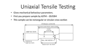
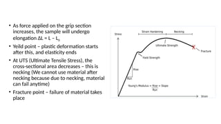
Uniaxial Tensile Testing
• Gives mechanical behaviour parameters.
• First you prepare sample by ASTM – E8/E8M
• This sample can be rectangular or circular cross section
• As force applied on the grip section
increases, the sample will undergo
elongation ΔL = L – L0
• Yeild point – plastic deformation starts
after this, and elasticity ends
• At UTS (Ultimate Tensile Stress), the
cross-sectional area decreases – this is
necking (We cannot use material after
necking because due to necking, material
can fail anytime)
• Fracture point – failure of material takes
place
You will get:
1) Young modulus: gives stiffness; slope of curve upto elastic point, we
will get young modulus; ability to resist elastic deformation
2) Toughness: Energy absorbed per unit volume = area under curve
upto fracture
3) Ductility: Elongation strain upto fracture; ability to undergo plastic
deformation
4) Resilience: Area under the curve upto elastic point
Our task:
• The tensile sample prepared from 3D printing was broken at the necking, and we need to analyse this
under the microscope, but for that, we need to cut it in small parts. We have two options to do this:
1) High-speed cutting machine: If we use high-speed cutting machine, then a lot of heat will be
generated and as the thickness of the blade is more, it will result in wastage of material. (Here,
water is the lubricant).
2) Low-speed cutting machine: If we use a low speed cutting machine, then material won't be wasted,
as blade is very thin, but more time is required. Here, oil is used as a lubricant to avoid friction
• Thus, for cutting tensile samples, we use low speed cutting machine, as our material is small, and less
material will be wasted.
• After the material is being cut, we will make a mould for it (using the moulding machine) so that we
will be able to hold it properly during polishing.
• This mould must be conducting because to analayse the microstructure, we will use SEM/FESEM, and
there, we require conducting material so that electron can strike on it.
• Thus, we make a mould of copper.
• We then polish it, and remove all the scratches present on it.
Additive Manufacturing (AM) Technology
• It is referred as three-dimensional printing technology which
produces objects layer-by layer (additively).
• Types of Processes:
1) Material Extrusion: Thermoplastic filament melted while pushed
through heated nozzle.
References: 1)
https://www.coursera.org/learn/introduction-to-additive-manufacturing-processes/lecture/s17yL/lecture-video-what-is-additive-
manufacturing
2) https://www.lboro.ac.uk/research/amrg/about/the7categoriesofadditivemanufacturing/
3)
Material Extrusion
Vat Photopolymerization
• Light hardens the liquid photopolymer resin into a solid.
• photopolymers in general do not have robust structural
characteristics, so the resulting parts are inherently more prone to
degradation and deformation over time. Additionally, printed parts
may require special handling or additional tooling depending on the
process and polymers used - making vat photopolymerization
prohibitively expensive for some applications.
References: 1)
https://www.plm.automation.siemens.com/global/en/our-story/glossary/vat-photopolymerization/53338
2)
Material Jetting
• Liquid is jetted and light or heat is used to cure metal.
Reference:
https://www.coursera.org/learn/introduction-to-additive-manufacturing-process
es/lecture/kEnJ2/lecture-video-additive-manufacturing-processes
Selective Laser Melting (SLM)- A Additive
Manufacturing Technique
• It was developed to produce metal components from metallic powders.
• It is a powder bed fusion process that uses high intensity laser (or electron beam) as an energy
source to melt and fuse selective regions of powder, layer by layer, according to computer aided
design (CAD) data. Binder materials are not required. There is a rapid solidification of material.
• The building chamber is filled with nitrogen or argon gas to protect the heated metals
against oxidation.
• Laser beams: CO2 laser (lambda = 10.6 micro m), Nd:YAG fibre laser (lambda = 1.06 micro m), Yb:
YAG fibre laser.
• One of the integral aspects of laser-material interaction is the absorptivity (absorption of energy
by the powder) of various materials to irradiation of different wavelengths. It was observed that
powder materials have higher absorptance in comparison to the bulk materials with smooth
surfaces.
Reference: https://pubs.aip.org/aip/apr/article/2/4/041101/123739/Review-of-selective-laser-melting-Materials-and
Reference:
Process
1) STereoLithography (STL) files are to be processed by softwares, such as Magics.
2) Laying a thin layer of metal powder (thickness ranges from 20 to 100 micro m) on a substrate plate in a building chamber.
3) After the powder is laid, a high energy density laser is used to melt and fuse selected areas according to the processed data.
4) Once the laser scanning is completed, the building platform is lowered, a next layer of powder is deposited on top and the laser
scans a new layer.
5) The process is then repeated for successive layers of powder until the required components are completely built.
6) Once the laser scanning process is completed, loose powders are removed from the building chamber and the component can be
separated from the substrate plate manually or by electrical discharge machining (EDM).
• Process parameters, such as laser power, scanning
speed, hatch spacing, and layer thickness,
are adjusted such that a single melt vector can fuse
completely with the neighbouring melt vectors and
the preceding layer.
• Reasons why we need proper parameters:
1) Insufficient energy, usually a combination of low
laser power, high scanning speed, and large
layer thickness, often results in balling due to lack
of wetting of molten pool with the preceding layer.
Balling might also occur if oxide film is formed on
the preceding layer which impedes interlayer
bonding. This can be reduced by keeping oxygen
level at 0.1%, applying a combination high laser
power and low scanning speed or applying re-
scanning of laser
2) High laser and low scanning speed may result in
extensive material evaporation and the keyhole
effect.
3) Poor hatch spacing often results in regular
porosity in built parts as adjacent melt lines do
not fuse together completely.
4) Moreover, vaporization in SLM often results in
condensation of volatilized materials on the laser
window, disrupting the delivery of laser power.
Laser and Material Interaction
Thermal fluctuations and its effects
• The materials experience varying degrees of thermal fluctuation
during the SLM process. This causes residual stress on the
components built. This mechanism can lead to crack formation.
• Methods to reduce residual stresses:
1) Sectorial Scanning: This strategy breaks down a layer into small
square grids and neighboring grids are scanned perpendicular to
one another.
Microstructure
• It gives us the properties of sample by their grain sizes and defects.
• It is necessary to use several types of microscopes, covering a wide
range of magnifications and resolutions:
1) Optical Microscope (Magnification: 0.2-1 µm)
2) Scanning Electron Microscope (SEM)
3) Transmission Electron Microscope (TEM)
References: 1) https://www.researchgate.net/publication/309744216_Microstructure_An_Introduction
How do you make an Electron Beam?
• pp
References: 1)
https://www.thermofisher.com/blog/materials/electron-source-fundamentals/#:~:text=Field%20emission%20
electrons,energy%20electrons%20to%20be%20released
Resolution in Microscopy
References: 1) https://youtu.be/4mfpvwbc2F4
2) https://youtu.be/sTa-Hn_eisw
3) https://www.giffgaff.com/blog/pixel-density-how-to-calculate-ppi/
Ppi: pixel per inch
Resolution One of the most important features of any microscope is its
resolving power, d (also referred to as the limit of resolution or simply
the resolution). The resolution is defined as the least separation
between two points at which they may be distinguished as separate
Optical Microscope (Magnification: 0.2-1 µm)
• In an optical microscope the light is incident on the sample and a
magnified image is produced.
• Resolving power:
• Lambda is the wavelength of the light, µ is the refractive index of the
medium between the sample and the objective lens, and α is one-half
the maximum angle of the light beam that is able to be collected by
the objective lens.
High angle/low angle grain boundaries
SEM
• In a scanning electron microscope (SEM), an electron beam is generated by
heating a tungsten filament, a lanthanum hexaboride (LaB6) crystal, or a field-
emission source, and this beam is focussed by electromagnetic lenses to form
the image.
• SEM imaging is much used in failure analysis for the examination of fracture
surfaces. The large depth of focus provides a three-dimensional (3D) appearance
of the fracture surfaces, and the fracture characteristics and topographies
provide essential information about the modes or causes of failures. In
particular, stereo pairs of fractographs, giving a full 3D effect, can be very useful
for detailed fractographic analyses.
References: 1)
https://www.thermofisher.com/blog/materials/electron-source-fundamentals/#:~:text=Field%20emission%20ele
ctrons,energy%20electrons%20to%20be%20released
.
Fracture Surfaces
References: 1) https://nte.mines-albi.fr/SciMat/en/co/SM6uc1-4.html
TEM
References: 1) https://www.unl.edu/ncmn-cfem/xzli/em/temoptic.htm
Microstructure
• The microstructure of the LPBF (Laser powder bed fusion) are significantly
distinct.
• The dislocation tangled cellular structure is one of the most significant
microstructural features in AM-fabricated alloys, which can remarkably
improve the strength and ductility simultaneously. Apart from cellular
structures, the microstructural features also include melt pool boundaries
(MPBs), columnar grains, highly serrated grain boundaries (GBs) and
nanoparticles, which in turn significantly affect the mechanical properties.
• Microstructural defects such as porosity leads to premature failure under
mechanical loading, but still ductility of 316L Stainless Steel (SS)
has improved a lot, and the ductility of an L-PBF SS increased by 130%.
• Dislocations:
1) Geometrically necessary dislocations (GNDs): GNDs are accumulated in plastic strain gradient fields caused by
local heterogeneous deformation, which are considered necessary to maintain the strain compatibility across
microstructures.
 The burger vector is net non-zero, which leads to an observed lattice curvature
1) Statistically stored dislocations (SSDs): SSDs are stored in the deformed polycrystalline aggregate through
random trapping processes
 Have a net zero burger vector, and thus, no lattice curvature
• In transmission electron microscopy (TEM) micrographs, the dislocation lines of both GNDs and SSDs could be
observed
• The total dislocation density is the sum of GND and SSD density, and both equally contribute to strength.
• The combined parameter energy density (ED) is
where PL, VL, HL and TL are laser power (W), scan speed (mm/s), hatch spacing (mm) and layer thickness (mm),
respectively.
Regular and uniform tracks are obtained when the ED value ranges from 87.5 to 140 J/mm3 resulting in a very low
porosity

Additive Manufacturing techniques presentation

  • 1.
    Uniaxial Tensile Testing •Gives mechanical behaviour parameters. • First you prepare sample by ASTM – E8/E8M • This sample can be rectangular or circular cross section
  • 2.
    • As forceapplied on the grip section increases, the sample will undergo elongation ΔL = L – L0 • Yeild point – plastic deformation starts after this, and elasticity ends • At UTS (Ultimate Tensile Stress), the cross-sectional area decreases – this is necking (We cannot use material after necking because due to necking, material can fail anytime) • Fracture point – failure of material takes place
  • 3.
    You will get: 1)Young modulus: gives stiffness; slope of curve upto elastic point, we will get young modulus; ability to resist elastic deformation 2) Toughness: Energy absorbed per unit volume = area under curve upto fracture 3) Ductility: Elongation strain upto fracture; ability to undergo plastic deformation 4) Resilience: Area under the curve upto elastic point
  • 4.
    Our task: • Thetensile sample prepared from 3D printing was broken at the necking, and we need to analyse this under the microscope, but for that, we need to cut it in small parts. We have two options to do this: 1) High-speed cutting machine: If we use high-speed cutting machine, then a lot of heat will be generated and as the thickness of the blade is more, it will result in wastage of material. (Here, water is the lubricant). 2) Low-speed cutting machine: If we use a low speed cutting machine, then material won't be wasted, as blade is very thin, but more time is required. Here, oil is used as a lubricant to avoid friction • Thus, for cutting tensile samples, we use low speed cutting machine, as our material is small, and less material will be wasted. • After the material is being cut, we will make a mould for it (using the moulding machine) so that we will be able to hold it properly during polishing. • This mould must be conducting because to analayse the microstructure, we will use SEM/FESEM, and there, we require conducting material so that electron can strike on it. • Thus, we make a mould of copper. • We then polish it, and remove all the scratches present on it.
  • 5.
    Additive Manufacturing (AM)Technology • It is referred as three-dimensional printing technology which produces objects layer-by layer (additively). • Types of Processes: 1) Material Extrusion: Thermoplastic filament melted while pushed through heated nozzle. References: 1) https://www.coursera.org/learn/introduction-to-additive-manufacturing-processes/lecture/s17yL/lecture-video-what-is-additive- manufacturing 2) https://www.lboro.ac.uk/research/amrg/about/the7categoriesofadditivemanufacturing/ 3)
  • 6.
  • 7.
    Vat Photopolymerization • Lighthardens the liquid photopolymer resin into a solid. • photopolymers in general do not have robust structural characteristics, so the resulting parts are inherently more prone to degradation and deformation over time. Additionally, printed parts may require special handling or additional tooling depending on the process and polymers used - making vat photopolymerization prohibitively expensive for some applications. References: 1) https://www.plm.automation.siemens.com/global/en/our-story/glossary/vat-photopolymerization/53338 2)
  • 8.
    Material Jetting • Liquidis jetted and light or heat is used to cure metal. Reference: https://www.coursera.org/learn/introduction-to-additive-manufacturing-process es/lecture/kEnJ2/lecture-video-additive-manufacturing-processes
  • 9.
    Selective Laser Melting(SLM)- A Additive Manufacturing Technique • It was developed to produce metal components from metallic powders. • It is a powder bed fusion process that uses high intensity laser (or electron beam) as an energy source to melt and fuse selective regions of powder, layer by layer, according to computer aided design (CAD) data. Binder materials are not required. There is a rapid solidification of material. • The building chamber is filled with nitrogen or argon gas to protect the heated metals against oxidation. • Laser beams: CO2 laser (lambda = 10.6 micro m), Nd:YAG fibre laser (lambda = 1.06 micro m), Yb: YAG fibre laser. • One of the integral aspects of laser-material interaction is the absorptivity (absorption of energy by the powder) of various materials to irradiation of different wavelengths. It was observed that powder materials have higher absorptance in comparison to the bulk materials with smooth surfaces. Reference: https://pubs.aip.org/aip/apr/article/2/4/041101/123739/Review-of-selective-laser-melting-Materials-and
  • 10.
  • 11.
    Process 1) STereoLithography (STL)files are to be processed by softwares, such as Magics. 2) Laying a thin layer of metal powder (thickness ranges from 20 to 100 micro m) on a substrate plate in a building chamber. 3) After the powder is laid, a high energy density laser is used to melt and fuse selected areas according to the processed data. 4) Once the laser scanning is completed, the building platform is lowered, a next layer of powder is deposited on top and the laser scans a new layer. 5) The process is then repeated for successive layers of powder until the required components are completely built. 6) Once the laser scanning process is completed, loose powders are removed from the building chamber and the component can be separated from the substrate plate manually or by electrical discharge machining (EDM).
  • 12.
    • Process parameters,such as laser power, scanning speed, hatch spacing, and layer thickness, are adjusted such that a single melt vector can fuse completely with the neighbouring melt vectors and the preceding layer. • Reasons why we need proper parameters: 1) Insufficient energy, usually a combination of low laser power, high scanning speed, and large layer thickness, often results in balling due to lack of wetting of molten pool with the preceding layer. Balling might also occur if oxide film is formed on the preceding layer which impedes interlayer bonding. This can be reduced by keeping oxygen level at 0.1%, applying a combination high laser power and low scanning speed or applying re- scanning of laser 2) High laser and low scanning speed may result in extensive material evaporation and the keyhole effect. 3) Poor hatch spacing often results in regular porosity in built parts as adjacent melt lines do not fuse together completely. 4) Moreover, vaporization in SLM often results in condensation of volatilized materials on the laser window, disrupting the delivery of laser power. Laser and Material Interaction
  • 13.
    Thermal fluctuations andits effects • The materials experience varying degrees of thermal fluctuation during the SLM process. This causes residual stress on the components built. This mechanism can lead to crack formation. • Methods to reduce residual stresses: 1) Sectorial Scanning: This strategy breaks down a layer into small square grids and neighboring grids are scanned perpendicular to one another.
  • 14.
    Microstructure • It givesus the properties of sample by their grain sizes and defects. • It is necessary to use several types of microscopes, covering a wide range of magnifications and resolutions: 1) Optical Microscope (Magnification: 0.2-1 µm) 2) Scanning Electron Microscope (SEM) 3) Transmission Electron Microscope (TEM) References: 1) https://www.researchgate.net/publication/309744216_Microstructure_An_Introduction
  • 15.
    How do youmake an Electron Beam? • pp References: 1) https://www.thermofisher.com/blog/materials/electron-source-fundamentals/#:~:text=Field%20emission%20 electrons,energy%20electrons%20to%20be%20released
  • 16.
    Resolution in Microscopy References:1) https://youtu.be/4mfpvwbc2F4 2) https://youtu.be/sTa-Hn_eisw 3) https://www.giffgaff.com/blog/pixel-density-how-to-calculate-ppi/ Ppi: pixel per inch Resolution One of the most important features of any microscope is its resolving power, d (also referred to as the limit of resolution or simply the resolution). The resolution is defined as the least separation between two points at which they may be distinguished as separate
  • 17.
    Optical Microscope (Magnification:0.2-1 µm) • In an optical microscope the light is incident on the sample and a magnified image is produced. • Resolving power: • Lambda is the wavelength of the light, µ is the refractive index of the medium between the sample and the objective lens, and α is one-half the maximum angle of the light beam that is able to be collected by the objective lens.
  • 18.
    High angle/low anglegrain boundaries
  • 19.
    SEM • In ascanning electron microscope (SEM), an electron beam is generated by heating a tungsten filament, a lanthanum hexaboride (LaB6) crystal, or a field- emission source, and this beam is focussed by electromagnetic lenses to form the image. • SEM imaging is much used in failure analysis for the examination of fracture surfaces. The large depth of focus provides a three-dimensional (3D) appearance of the fracture surfaces, and the fracture characteristics and topographies provide essential information about the modes or causes of failures. In particular, stereo pairs of fractographs, giving a full 3D effect, can be very useful for detailed fractographic analyses. References: 1) https://www.thermofisher.com/blog/materials/electron-source-fundamentals/#:~:text=Field%20emission%20ele ctrons,energy%20electrons%20to%20be%20released .
  • 20.
    Fracture Surfaces References: 1)https://nte.mines-albi.fr/SciMat/en/co/SM6uc1-4.html
  • 21.
  • 22.
    Microstructure • The microstructureof the LPBF (Laser powder bed fusion) are significantly distinct. • The dislocation tangled cellular structure is one of the most significant microstructural features in AM-fabricated alloys, which can remarkably improve the strength and ductility simultaneously. Apart from cellular structures, the microstructural features also include melt pool boundaries (MPBs), columnar grains, highly serrated grain boundaries (GBs) and nanoparticles, which in turn significantly affect the mechanical properties. • Microstructural defects such as porosity leads to premature failure under mechanical loading, but still ductility of 316L Stainless Steel (SS) has improved a lot, and the ductility of an L-PBF SS increased by 130%.
  • 23.
    • Dislocations: 1) Geometricallynecessary dislocations (GNDs): GNDs are accumulated in plastic strain gradient fields caused by local heterogeneous deformation, which are considered necessary to maintain the strain compatibility across microstructures.  The burger vector is net non-zero, which leads to an observed lattice curvature 1) Statistically stored dislocations (SSDs): SSDs are stored in the deformed polycrystalline aggregate through random trapping processes  Have a net zero burger vector, and thus, no lattice curvature • In transmission electron microscopy (TEM) micrographs, the dislocation lines of both GNDs and SSDs could be observed • The total dislocation density is the sum of GND and SSD density, and both equally contribute to strength. • The combined parameter energy density (ED) is where PL, VL, HL and TL are laser power (W), scan speed (mm/s), hatch spacing (mm) and layer thickness (mm), respectively. Regular and uniform tracks are obtained when the ED value ranges from 87.5 to 140 J/mm3 resulting in a very low porosity