The document provides an overview of AD/DA conversion techniques. It discusses what AD and DA converters are, how they work, and some of their common applications. It then covers various conversion methods like successive approximation, flash, integrating, sigma-delta, as well as digital coding methods and sources of error in waveform digitization. Examples of AD/DA applications at CERN are also presented involving applications from low to high speed. Key circuits like sample and hold, R-2R ladders for DACs, and basic ADC designs are reviewed.
![What are AD/DA
Converters (1)
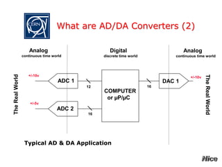
An Analog to Digital converter [AD or ADC]
is an electronic circuit which accepts an
analog input signal (usually a voltage) and
produces a corresponding digital number at
the output
An Digital to Analog converter [DA or DAC]
is an electronic circuit which accepts a
digital number at its input and produces a
corresponding analog signal (usually a
voltage) at the output
They exist as modules, ICs, or fully
integrated inside other parts, e.g. µCs](https://image.slidesharecdn.com/addalecturep1-230521012812-bd1e2c8c/85/ADDA_Lecture_P1-ppt-4-320.jpg)
![Digital coding methods (1)
8,10,12,14,16,18, 20-24bits?
Most/Least significant bit
MSB/LSB
Uni-polar, bipolar, straight
binary, 2’s complement -
invert MSB
Parallel I/O or serial [delay]
Bytes or words
Double buffering
Digital ‘breakthrough’
Digital correction methods
Time skewing & jitter
0v
+10v
-10v
0000 FFFF
8000
AD/DA Transfer Characteristic
0000 7FFF
FFFF
8000](https://image.slidesharecdn.com/addalecturep1-230521012812-bd1e2c8c/85/ADDA_Lecture_P1-ppt-9-320.jpg)
![Digital coding methods (2)
Resolution = 2n-1 [n = number of bits]
n 2n 1bit ppm [1x10⁻⁶]
8bits 256 3906
10bits 1024 976
12bits 4096 244
14bits 16384 61
16bits 65536 15
18bits 262144 3.8
20bits 1,048576 0.95
22bits 4,194304 0.24
24bits 16,777216 0.06](https://image.slidesharecdn.com/addalecturep1-230521012812-bd1e2c8c/85/ADDA_Lecture_P1-ppt-10-320.jpg)
![Waveform digitising (1)
A waveform is ‘digitised’ (sampled) at a constant
rate D t
Each such sample represents the instantaneous
amplitude at the instant of sampling
Between samples the value remains constant [zero
order hold]
What errors can occur in this process ?
time
Digital
value](https://image.slidesharecdn.com/addalecturep1-230521012812-bd1e2c8c/85/ADDA_Lecture_P1-ppt-11-320.jpg)
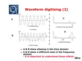
![Waveform digitising errors
For a DAC
output waveform is a ‘distorted’ version of original
higher frequencies not reproduced - aliasing ?
‘average shape’ displaced in time
‘sharp’ edges need filtering
For an ADC
converter sampling errors
with a ‘sample & hold’ circuit ahead of the converter?
integrating action during part, or all of the sample-time
?
conversion time
data ‘available’ delay
aliasing - [ is multiplication of input spectrum and
fs]
…[must ‘remove’ all spectrum > fs/2 before
sampling]](https://image.slidesharecdn.com/addalecturep1-230521012812-bd1e2c8c/85/ADDA_Lecture_P1-ppt-13-320.jpg)
![Sampling rate
Nyquist rate = 2x highest frequency of
interest
Practically, - always sample at least 5x, or
higher
Ensure ADCs have input filtering [anti-alias]
where necessary [large hf signals]
Filter DAC outputs to remove higher
frequencies and switching ‘glitches’
‘Over-sampling’ converters sample x4 to
x500 - this may reduce above problems
and/or extend resolution](https://image.slidesharecdn.com/addalecturep1-230521012812-bd1e2c8c/85/ADDA_Lecture_P1-ppt-14-320.jpg)
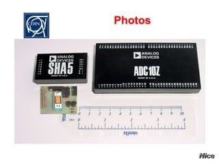
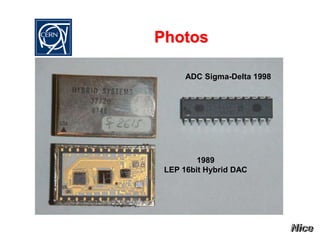
![Photos
1969
ISR Beam-Transfer DAC
[5 decimal decades]
Relay switching
Kelvin-Varley divider
1973
ISR Main Bends DAC
[16bit binary
All electronic switching](https://image.slidesharecdn.com/addalecturep1-230521012812-bd1e2c8c/85/ADDA_Lecture_P1-ppt-16-320.jpg)

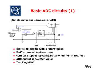
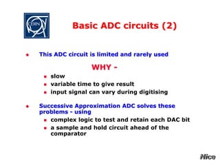
![Some very simple ideas
ADC =
precise reference voltage
comparison of divider value with unknown [analog input]
“digitally adjustable” divider or potentiometer [output
value]
DAC =
precise reference voltage ……. {multiplying dac}
“digitally adjustable” divider or potentiometer [input
value]
optional output amplifier of pot. value [analog output]
=
‘Digitally set’
potentiometer
dial
Comparator
equal
Vref
Unknown
voltage
DAC ADC
Vdac](https://image.slidesharecdn.com/addalecturep1-230521012812-bd1e2c8c/85/ADDA_Lecture_P1-ppt-20-320.jpg)
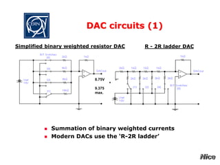
![DAC circuits (2)
Important circuit concepts
Resistor tracking - temp. & time > ratios
Switch is part of R [on & off resistance]
Limits for tracking and adjustment
Switch transition times - glitches
Switched current sources are faster
Other DAC methods
DC performance not needed for all uses
Different ladders, Caps. as well as Resistors
PWM, F>V
Sigma-Delta
Performance cannot be better than the Reference
- {multiplying DAC concept}](https://image.slidesharecdn.com/addalecturep1-230521012812-bd1e2c8c/85/ADDA_Lecture_P1-ppt-22-320.jpg)
![Sample & Hold Circuit (1)
Essential for defining the ‘exact’ moment of
sampling
Circuit introduces other error sources [ see (2) ]
LF398](https://image.slidesharecdn.com/addalecturep1-230521012812-bd1e2c8c/85/ADDA_Lecture_P1-ppt-27-320.jpg)