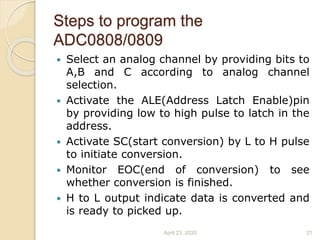
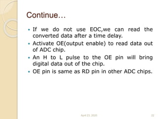
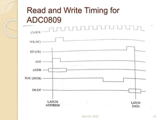
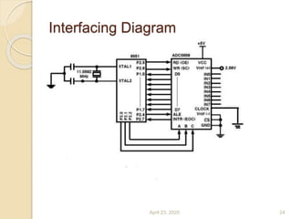
Dr. Vithalrao Vikhe Patil College of Engineering,
Ahmednagar
Department of Information Technology
Lecture on
Unit No 6
ADC Interfacing with 8051 Microcontroller
Processor Architecture & Interfacing (S.E.I.T.)
Presentation By
Prof. Ms. M. S. Gunjal
Department of Information Technology
Objectives
 What is ADC
 Pin diagram of ADC0804
 Pin description of ADC0804
 Interfacing Diagram of ADC with 8051
 Working of ADC
 Timing Diagram
 ADC0808/0809
April 23, 2020 2
 ADC Stands for “Analog to Digital Conversion"
 ADC converts the given analog value to a
digital value .
 Sensors and transducers used in industry are
analog in nature.
 It is necessary to convert the analog output
from the sensors to digital so that the
corresponding signal can be processed by the
controller.
ADC?
April 23, 2020 3
Continue…
 ADCs are used everywhere when we have to
process, store or transmit an analog signal
in digital form.
 ADCs are used in TV tuner cards.
 There are lot of digital ICs available to
convert analog to digital.
 In Microcontroller interfacing the frequently
used ICs are 0804 and 0808
 ADC chips are either parallel or serial.
April 23, 2020 4
ADC0804
 The ADC0804 IC is 20 Pin 8-bit parallel ADC.
 It works with +5volts and has a resolution of
8 bits.
 The ADC0804 is a commonly used ADC
module, for projects where an external ADC
is required.
 In this ADC the conversion time varies
depending on the clocking signals applied to
CLK IN pin.
 But the conversion time cannot be faster
than 110 microseconds.
April 23, 2020 5
Features of ADC0804 Family:
 8-bit resolution ADC
 Conversion time 110 μs
 Access time 135 ns.
 It has an on-chip clock generator.
 It does not require any zero adjustment.
 It operates on single 5V power supply.
 Output meet TTL voltage level specifications.
April 23, 2020 6
ADC0804 chip Pin diagram
April 23, 2020 7
Pin Diagram Description
Pin Symbol Descriptions
1 CS# Chip select is an active low input used to
activate the ADC0804 chip.
2 RD This is active low input signal. RD (Read)
Make this pin high(1) and after some time
low(0). This will bring data from internal
registers to the output pins after conversion
3 WR WR (Write) Make this pin low(0) to high(1) to
start conversion of data(analog to digital)
4 CLK IN Clock IN (CLK IN) Connect external clock to
this pin.
5 INTR# Interrupt (INTR) This pin automatically goes
low when conversion is done by ADC0804 or
when digital equivalent of analog input is
ready.
6 Vin(+) Vin (+) connect input analog sensor pin/input
voltage to this pin.
7 Vin(-) Vin (-) ground this pin.
April 23, 2020 8
Continue…
Pin Symbol Description
8 AGND AnalogGround (AGND) ground this pin.
9 Vref/2 Vref/2 set the reference voltage for analog
input(Very important pin discussed further)
10 DGND DigitalGround (DGND) ground this pin
11 to
18
D0 t0 D7 PIN 11 TO 18 ARE DATA PINS OUTPUT DATA
PINS
19 CLK R Clock R (CLK R) Used with clock IN pin when
internal clock source is used
20 Vcc +5 volts
April 23, 2020 9
ADC0804 reference pin (Vref/2)
 Vref/2 is voltage reference pin of ADC0804.
Reference means that after this much
amount of voltage change at input, output
must increase by 1 or the set limit.
 Vref/2 (pin-9) left open means input
voltage span is 0-5 volts and step size is
5/256=19.53 mV.
 Voltage span means that the ADC can
measure in the range for example for the
above case from 0-5 volts.
 step size it mean’s after the rise of 19.53 mv
at input the output increases by one unit. If
now output is 2 then after 19.53 mv
increase in input voltage output will be 3.
April 23, 2020 10
Different Vref/2 voltages and
corresponding analogue input voltage
spans.
Vref/2 (pin 9) Volts Input Voltage (volt) Step size(mv)
Left open 0-5 5/256=19.53
2 0-4 4/256=15.62
1.5 0-3 3/256=11.71
1.28 0-2.56 2.56/256=10
1.0 0-2 2/256=7.812
0.5 0-1 1/256=3.906
April 23, 2020 11
Interfacing Diagram
April 23, 2020 12
Working of ADC…
 For every interfacing initialization is needed.
 For ADC the initial values are
 INTR=1; // interrupt for completion of ADC
process
 rd=1; // read from 0804
 wr=0; // start conversion write..
 Next step is to start the process of
converting analog voltage to digital data
 By changing the state of the write pin
transition from 0 to 1 will start the
conversion.
 End of conversion will be acknowledged by
a change in the INTR state.
April 23, 2020 13
Steps for converting the analogue
input and reading the output from
ADC0804.
 Make CS=0 and send a low to high pulse to
WR pin to start the conversion.
 Now keep checking the INTR pin.
 If conversion is not finished (INTR=1) , poll
until it is finished.
 If conversion is finished (INTR=0), go to the
next step.
 Make CS=0 and send a high to low pulse to
RD pin to read the data from the ADC.
April 23, 2020 14
Timing Diagram
April 23, 2020 15
ADC0808/0809
 ADC 0809 is an 8 channel, 8 bit ADC.
 It can convert an analog voltage input into
an 8 bit digital data output.
 To select an input out of 8 options, there are
three select lines (C, B and A).
 We put a channel number on these lines
(0…7) and latch it using ALE.
 SC signal is given to indicate start of
conversion.
 Reference voltage for conversion is provided
using +Vref and –Vref. The clock supply
needed for conversion is given through CLK
(typically ~ 1MHz).
April 23, 2020 16
ADC0808/0809
 The end of conversion is indicated by the
ADC using EOC signal.
 There is no Vref/2 in the ADC0808/0809
chip.
April 23, 2020 17
ADC0808/0809
April 23, 2020 18
Analog Channel Selection
Selected Analog
Channel
C B A
IN0 0 0 0
IN1 0 0 1
IN2 0 1 0
IN3 0 1 1
IN4 1 0 0
IN5 1 0 1
IN6 1 1 0
IN7 1 1 1
April 23, 2020 19
Vref Relation to Vin
Vref (V) Vin (V) Step Size (mv)
Not Connected 0 to 5 5/256=19.53
4.0 0 to 4 4/256=15.62
3.0 0 to 3 3/256=11.71
2.56 0 to 2.56 2.56/256=10
2.0 0 to 2 2/256=7.81
1.0 0 to 1 1/256=3.90
April 23, 2020 20
Steps to program the
ADC0808/0809
 Select an analog channel by providing bits to
A,B and C according to analog channel
selection.
 Activate the ALE(Address Latch Enable)pin
by providing low to high pulse to latch in the
address.
 Activate SC(start conversion) by L to H pulse
to initiate conversion.
 Monitor EOC(end of conversion) to see
whether conversion is finished.
 H to L output indicate data is converted and
is ready to picked up.
April 23, 2020 21
Continue…
 If we do not use EOC,we can read the
converted data after a time delay.
 Activate OE(output enable) to read data out
of ADC chip.
 An H to L pulse to the OE pin will bring
digital data out of the chip.
 OE pin is same as RD pin in other ADC chips.
April 23, 2020 22
Read and Write Timing for
ADC0809
April 23, 2020 23
Interfacing Diagram
April 23, 2020 24
Thank You !!!
April 23, 2020 25

Adc interfacing

  • 1.
    Dr. Vithalrao VikhePatil College of Engineering, Ahmednagar Department of Information Technology Lecture on Unit No 6 ADC Interfacing with 8051 Microcontroller Processor Architecture & Interfacing (S.E.I.T.) Presentation By Prof. Ms. M. S. Gunjal Department of Information Technology
  • 2.
    Objectives  What isADC  Pin diagram of ADC0804  Pin description of ADC0804  Interfacing Diagram of ADC with 8051  Working of ADC  Timing Diagram  ADC0808/0809 April 23, 2020 2
  • 3.
     ADC Standsfor “Analog to Digital Conversion"  ADC converts the given analog value to a digital value .  Sensors and transducers used in industry are analog in nature.  It is necessary to convert the analog output from the sensors to digital so that the corresponding signal can be processed by the controller. ADC? April 23, 2020 3
  • 4.
    Continue…  ADCs areused everywhere when we have to process, store or transmit an analog signal in digital form.  ADCs are used in TV tuner cards.  There are lot of digital ICs available to convert analog to digital.  In Microcontroller interfacing the frequently used ICs are 0804 and 0808  ADC chips are either parallel or serial. April 23, 2020 4
  • 5.
    ADC0804  The ADC0804IC is 20 Pin 8-bit parallel ADC.  It works with +5volts and has a resolution of 8 bits.  The ADC0804 is a commonly used ADC module, for projects where an external ADC is required.  In this ADC the conversion time varies depending on the clocking signals applied to CLK IN pin.  But the conversion time cannot be faster than 110 microseconds. April 23, 2020 5
  • 6.
    Features of ADC0804Family:  8-bit resolution ADC  Conversion time 110 μs  Access time 135 ns.  It has an on-chip clock generator.  It does not require any zero adjustment.  It operates on single 5V power supply.  Output meet TTL voltage level specifications. April 23, 2020 6
  • 7.
    ADC0804 chip Pindiagram April 23, 2020 7
  • 8.
    Pin Diagram Description PinSymbol Descriptions 1 CS# Chip select is an active low input used to activate the ADC0804 chip. 2 RD This is active low input signal. RD (Read) Make this pin high(1) and after some time low(0). This will bring data from internal registers to the output pins after conversion 3 WR WR (Write) Make this pin low(0) to high(1) to start conversion of data(analog to digital) 4 CLK IN Clock IN (CLK IN) Connect external clock to this pin. 5 INTR# Interrupt (INTR) This pin automatically goes low when conversion is done by ADC0804 or when digital equivalent of analog input is ready. 6 Vin(+) Vin (+) connect input analog sensor pin/input voltage to this pin. 7 Vin(-) Vin (-) ground this pin. April 23, 2020 8
  • 9.
    Continue… Pin Symbol Description 8AGND AnalogGround (AGND) ground this pin. 9 Vref/2 Vref/2 set the reference voltage for analog input(Very important pin discussed further) 10 DGND DigitalGround (DGND) ground this pin 11 to 18 D0 t0 D7 PIN 11 TO 18 ARE DATA PINS OUTPUT DATA PINS 19 CLK R Clock R (CLK R) Used with clock IN pin when internal clock source is used 20 Vcc +5 volts April 23, 2020 9
  • 10.
    ADC0804 reference pin(Vref/2)  Vref/2 is voltage reference pin of ADC0804. Reference means that after this much amount of voltage change at input, output must increase by 1 or the set limit.  Vref/2 (pin-9) left open means input voltage span is 0-5 volts and step size is 5/256=19.53 mV.  Voltage span means that the ADC can measure in the range for example for the above case from 0-5 volts.  step size it mean’s after the rise of 19.53 mv at input the output increases by one unit. If now output is 2 then after 19.53 mv increase in input voltage output will be 3. April 23, 2020 10
  • 11.
    Different Vref/2 voltagesand corresponding analogue input voltage spans. Vref/2 (pin 9) Volts Input Voltage (volt) Step size(mv) Left open 0-5 5/256=19.53 2 0-4 4/256=15.62 1.5 0-3 3/256=11.71 1.28 0-2.56 2.56/256=10 1.0 0-2 2/256=7.812 0.5 0-1 1/256=3.906 April 23, 2020 11
  • 12.
  • 13.
    Working of ADC… For every interfacing initialization is needed.  For ADC the initial values are  INTR=1; // interrupt for completion of ADC process  rd=1; // read from 0804  wr=0; // start conversion write..  Next step is to start the process of converting analog voltage to digital data  By changing the state of the write pin transition from 0 to 1 will start the conversion.  End of conversion will be acknowledged by a change in the INTR state. April 23, 2020 13
  • 14.
    Steps for convertingthe analogue input and reading the output from ADC0804.  Make CS=0 and send a low to high pulse to WR pin to start the conversion.  Now keep checking the INTR pin.  If conversion is not finished (INTR=1) , poll until it is finished.  If conversion is finished (INTR=0), go to the next step.  Make CS=0 and send a high to low pulse to RD pin to read the data from the ADC. April 23, 2020 14
  • 15.
  • 16.
    ADC0808/0809  ADC 0809is an 8 channel, 8 bit ADC.  It can convert an analog voltage input into an 8 bit digital data output.  To select an input out of 8 options, there are three select lines (C, B and A).  We put a channel number on these lines (0…7) and latch it using ALE.  SC signal is given to indicate start of conversion.  Reference voltage for conversion is provided using +Vref and –Vref. The clock supply needed for conversion is given through CLK (typically ~ 1MHz). April 23, 2020 16
  • 17.
    ADC0808/0809  The endof conversion is indicated by the ADC using EOC signal.  There is no Vref/2 in the ADC0808/0809 chip. April 23, 2020 17
  • 18.
  • 19.
    Analog Channel Selection SelectedAnalog Channel C B A IN0 0 0 0 IN1 0 0 1 IN2 0 1 0 IN3 0 1 1 IN4 1 0 0 IN5 1 0 1 IN6 1 1 0 IN7 1 1 1 April 23, 2020 19
  • 20.
    Vref Relation toVin Vref (V) Vin (V) Step Size (mv) Not Connected 0 to 5 5/256=19.53 4.0 0 to 4 4/256=15.62 3.0 0 to 3 3/256=11.71 2.56 0 to 2.56 2.56/256=10 2.0 0 to 2 2/256=7.81 1.0 0 to 1 1/256=3.90 April 23, 2020 20
  • 21.
    Steps to programthe ADC0808/0809  Select an analog channel by providing bits to A,B and C according to analog channel selection.  Activate the ALE(Address Latch Enable)pin by providing low to high pulse to latch in the address.  Activate SC(start conversion) by L to H pulse to initiate conversion.  Monitor EOC(end of conversion) to see whether conversion is finished.  H to L output indicate data is converted and is ready to picked up. April 23, 2020 21
  • 22.
    Continue…  If wedo not use EOC,we can read the converted data after a time delay.  Activate OE(output enable) to read data out of ADC chip.  An H to L pulse to the OE pin will bring digital data out of the chip.  OE pin is same as RD pin in other ADC chips. April 23, 2020 22
  • 23.
    Read and WriteTiming for ADC0809 April 23, 2020 23
  • 24.
  • 25.