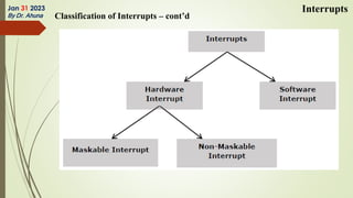
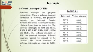
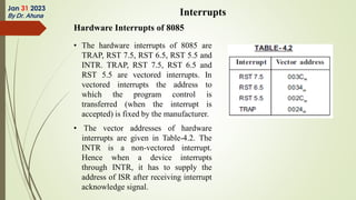
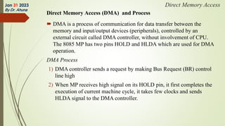
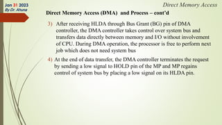
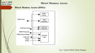
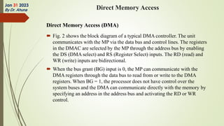
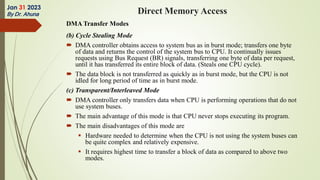
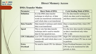
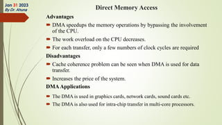
Topic 5a
[1] 8085 Interrupts
[2] Direct Memory Access
Feb 06 2024
By Dr. Ahuna
Interrupt and its Need
 An Interrupt is a signal send by an external device to the processor, for the
processor to perform a given task or work. In general, an interrupt is the process of
interrupting the normal program execution to carry out a specific task/work.
 In the microprocessor based system interrupts are used for data transfer between the
peripheral devices and the microprocessor.
 When a peripheral is ready for data transfer, it interrupts the processor by sending
an appropriate signal to the interrupt pin of the processor. If the processor accepts
the interrupt then the processor suspends its current activity and executes an
interrupt service subroutine to complete the data transfer between the peripheral
and processor.
 After executing the interrupt service routine the processor resumes its current
activity. This type of data transfer scheme is called interrupt driven data transfer
scheme.
Interrupts
Ways of Interrupting the microprocessor
 A processor can be interrupted in the following ways :
1) by an external signal generated by a peripheral,
2) by an internal signal generated by a special instruction in the
program,
3) by an internal signal generated due to an exceptional condition
which occurs while executing an instruction.
 When a microprocessor receives an interrupt signal, it stops executing
the current normal program, saves the status (or content) of various
registers (PC in case of 8085) in stack and then executes a
subroutine/procedure in order to perform the specific task/work
requested by the interrupt.
Jan 31 2023
By Dr. Ahuna Interrupts
Ways of Interrupting the microprocessor – cont’d
 The subroutine/procedure that is executed in response to an interrupt
is also called Interrupt Service Routine (ISR). At the end of ISR, the
stored status of registers in stack are restored to respective registers
and the processor resumes the normal program execution from the
point (instruction) where it was interrupted.
 The external interrupts are used to implement interrupt driven data
transfer scheme. The interrupts generated by special instructions are
called software interrupts and they are used to implement system
services/calls (or monitor services/calls). The system /monitor
services are procedures developed by the system designer for various
operations and stored in memory. The user can call these services
through software interrupts.
Jan 31 2023
By Dr. Ahuna Interrupts
Classification of Interrupts
 In general interrupts can be classified in the following three ways :
1) Hardware and software interrupts.
2) Maskable and non-maskable interrupts.
3) Vectored and non-vectored interrupts.
Hardware Interrupts
 Interrupts initiated by external hardware by sending an appropriate signal to
the interrupt pin of the processor is called hardware interrupt. The 8085
processor has five interrupt pins TRAP, RST 7.5, RST 6.5, RST 5.5 and
INTR and the interrupts initiated by applying appropriate signal to these
pins are called hardware interrupts of 8085.
Jan 31 2023
By Dr. Ahuna Interrupts
Classification of Interrupts – cont’d
Jan 31 2023
By Dr. Ahuna
Interrupts
Software Interrupts Of 8085
Jan 31 2023
By Dr. Ahuna Interrupts
Software interrupts are program
instructions. When a software interrupt
instruction is executed, the processor
executes an Interrupt Service
Routine(ISR) stored in the vector address
of that software interrupt instruction. The
software interrupts of 8085 are RST0,
RST1, RST2, RST3, RST4, RST5, RST6
and RST7. The software interrupts of
8085 are vectored interrupts. Software
interrupts cannot be masked or be
disabled. The Vector addresses of
software interrupts are given in Table-
4.1.
Hardware Interrupts of 8085
Jan 31 2023
By Dr. Ahuna Interrupts
• The hardware interrupts of 8085 are
TRAP, RST 7.5, RST 6.5, RST 5.5 and
INTR. TRAP, RST 7.5, RST 6.5 and
RST 5.5 are vectored interrupts. In
vectored interrupts the address to
which the program control is
transferred (when the interrupt is
accepted) is fixed by the manufacturer.
• The vector addresses of hardware
interrupts are given in Table-4.2. The
INTR is a non-vectored interrupt.
Hence when a device interrupts
through INTR, it has to supply the
address of ISR after receiving interrupt
acknowledge signal.
Hardware Interrupts of 8085 – cont’d
 TRAP is a non-maskable interrupt and RST 7.5, RST 6.5 and RST 5.5 are
maskable interrupts, which use the SIM (Set Interrupt Mask) instruction.
Interrupts can be masked by moving an appropriate data (or code) to the
accumulator and then executing the SIM instruction.
 The status of maskable interrupts can be read into the accumulator by
executing the RIM instruction (RIM - Read Interrupt Mask).
 All the hardware interrupts, except TRAP are disabled when the processor
is reset and they can also be disabled by executing the DI instruction. (DI -
Disable Interrupt).
 When an interrupt is disabled, it will not be accepted by the processor (i.e.,
INTR, RST 5.5, RST 6.5 and RST 7.5 are disabled by the DI instruction
and upon hardware reset). In order to enable (or to allow) the disabled
interrupts, the processor has to execute the EI instruction (EI - Enable
Interrupt).
Jan 31 2023
By Dr. Ahuna
Interrupts
Vectored Interrupts & Non-Vectored Interrupts
 When an interrupt signal is accepted by the processor, and the program
control automatically branches to a specific address (called vector address)
then the interrupt is called vectored interrupt.
 All the 8085 interrupts except INTR are vectored interrupts.
 The automatic branching to a vector address is predefined by the
manufacturer of the processor. (In these vector addresses the interrupt
service subroutines (ISR) are stored.)
 In non-vectored interrupts the interrupting device should supply the
address of the ISR to be executed in response to the interrupt.
Jan 31 2023
By Dr. Ahuna
Interrupts
Maskable & Non-Maskable Interrupts
 Processors have the facility for accepting or rejecting hardware interrupts. Programming
the processor to reject an interrupt is referred to as masking or disabling and
programming the processor to accept an interrupt is referred to as unmasking or enabling.
 Interrupts whose request can be either accepted or rejected by the processor are called
maskable interrupts. Interrupts whose request has to be definitely accepted (i.e., it cannot
be rejected) by the processor are called non-maskable interrupts.
 In 8085, the hardware interrupts RST 7.5, RST 6.5, and RST 5.5 can be
masked/unmasked using the SIM instruction. All hardware interrupts except TRAP are
disabled by executing DI instruction and they are enabled by executing EI instruction.
 Whenever a request is made by a non-maskable interrupt, the processor has to definitely
accept that request and service that interrupt by suspending its current program and
executing an ISR.
 In 8085 processor all the hardware interrupts except TRAP are maskable. The interrupt
initiated through TRAP pin and all software interrupts are non-maskable.
Jan 31 2023
By Dr. Ahuna
Interrupts
Maskable & Non-Maskable Interrupts – cont’d
 All the hardware interrupts except TRAP are disabled by executing DI
instruction and they are enabled by executing EI instruction.
 Interrupts whose request can be either accepted or rejected by the
processor are called maskable interrupts. Interrupts whose request has to
be definitely accepted (i.e., it cannot be rejected) by the processor are
called non-maskable interrupts.
 Whenever a request is made by a non-maskable interrupt, the processor
has to definitely accept that request and service that interrupt by
suspending its current program and executing an ISR.
 In 8085 processor all the hardware interrupts except TRAP are maskable.
The interrupt initiated through TRAP pin and all software interrupts are
non-maskable.
Jan 31 2023
By Dr. Ahuna
Interrupts
Priorities of Interrupts
 When all the interrupts are enabled, the priority sequence of hardware
interrupts from highest to lowest is TRAP, RST 7.5, RST 6.5, RST 5.5 and
INTR. When the 8085 processor accepts an interrupt it will disable all the
hardware interrupts except TRAP.
 Hence in order to allow the higher priority interrupt while executing
Interrupt Service Subroutine (ISR) for lower priority interrupt, enable the
interrupt system in the beginning of ISR of lower priority interrupt, by
executing EI instruction.
 For example, if the processor accepts RST 5.5 interrupt, then it will disable
RST 7.5, RST 6.5 and INTR interrupts. In order to allow the higher priority
interrupt RST 7.5 and RST 6.5 while executing ISR of RST 5.5, the EI
instruction should be executed in the beginning of ISR of RST 5.5.
 The execution of software interrupt will not disable any hardware interrupt.
Therefore while executing ISR of software interrupts, the processor will
recognize or allow the hardware interrupts.
Jan 31 2023
By Dr. Ahuna Interrupts
TRAP
RST 7.5
RST 6.5
RST 5.5
INTR
Enabling, Disabling & Masking 8085 Interrupts
TRAP
 The interrupt TRAP is non-maskable and it cannot be disabled by DI
instruction. Also the TRAP is not disabled by system (processor) reset or
after recognition of another interrupt. The only signal which can override
TRAP is HOLD signal. (i.e., If the processor receives HOLD and TRAP at
the same time then HOLD is recognized first and only then is TRAP
recognized.)
INTR
 The interrupt INTR is disabled by any one of the following operations:
 Executing DI instruction.
 System or processor reset.
 After recognition (acceptance) of an interrupt.
 The interrupt INTR can be enabled by executing EI instruction.
Jan 31 2023
By Dr. Ahuna Interrupts
TRAP
RST 7.5
RST 6.5
RST 5.5
INTR
Enabling, Disabling & Masking 8085 Interrupts
RST 7.5, RST 6.5 and RST 5.5
 The interrupt RST 7.5, RST 6.5 and RST 5.5 are disabled by any one of the
following operations.
 Executing DI instruction.
 System or processor reset.
 After recognition (acceptance) of an interrupt.
 These hardware interrupts can be enabled by executing EI instruction.
 The 8085 provides additional masking facility for RST 7.5, RST 6.5 and
RST 5.5 using SIM instruction. The status of these interrupts can be read by
executing RIM instruction.
Jan 31 2023
By Dr. Ahuna Interrupts
The masking or unmasking of RST 7.5, RST 6.5 and RST 5.5 interrupts can be performed
by moving an 8-bit data to accumulator and then executing SIM instruction. The format of
the 8-bit data is shown in Fig. 4.1.
Jan 31 2023
By Dr. Ahuna
RST 7.5, RST 6.5 and RST 5.5 – cont’d
The status of pending interrupts can be read from accumulator after executing RIM
instruction. When RIM instruction is executed, an 8-bit data is loaded to the accumulator,
which can be interpreted as shown in Fig. 4.2.
Jan 31 2023
By Dr. Ahuna
Interrupts – cont’d
RST 7.5, RST 6.5 and RST 5.5 – cont’d
EXAMPLE 1
 Write a program segment to mask RST 6.5 and RST 5.5 interrupts and enable RST 7.5
interrupt.
Solution
 The 8-bit data format to be loaded in the accumulator for enabling RST 7.5 and
masking RST 6.5 and RST 5.5 is shown below. The data to be loaded in accumulator
is 0BH.
Jan 31 2023
By Dr. Ahuna
Interrupts – cont’d
RST 7.5, RST 6.5 and RST 5.5 – cont’d
EXAMPLE 1
Program Segment
Jan 31 2023
By Dr. Ahuna
Interrupts – cont’d
RST 7.5, RST 6.5 and RST 5.5 – cont’d
EXAMPLE 2
 Assume that the 8085 microprocessor returns to the main program after servicing RST
6.5. (Remember that while servicing an interrupt all other interrupts are disabled.)
 Write a program segment to check whether RST 5.5 interrupt is pending. If it is
pending then the program has to enable RST 5.5 without affecting any other
interrupts. Otherwise the program has to enable all interrupts and return to main
program.
Solution
 The status of pending interrupts can be read by executing RIM instruction. This will
load an 8-bit data in accumulator. If RST 5.5 is pending then the bit D4 in accumulator
will be 1 and if it is not pending then bit D4 will be 0.
 The following program segment have been written to check whether bit D4 is 1 or 0.
If it is 1 then the program control jumps to another part of program to enable RST 5.5
and mask other interrupts.
Jan 31 2023
By Dr. Ahuna
Interrupts – cont’d
RST 7.5, RST 6.5 and RST 5.5 – cont’d
EXAMPLE 2
Jan 31 2023
By Dr. Ahuna
Interrupts – cont’d
Direct Memory Access
Direct Memory Access (DMA) and Process
 DMA is a process of communication for data transfer between the
memory and input/output devices (peripherals), controlled by an
external circuit called DMA controller, without involvement of CPU.
The 8085 MP has two pins HOLD and HLDA which are used for DMA
operation.
DMA Process
1) DMA controller sends a request by making Bus Request (BR) control
line high
2) When MP receives high signal on its HOLD pin, it first completes the
execution of current machine cycle, it takes few clocks and sends
HLDA signal to the DMA controller.
Jan 31 2023
By Dr. Ahuna
Direct Memory Access
Direct Memory Access (DMA) and Process – cont’d
3) After receiving HLDA through Bus Grant (BG) pin of DMA
controller, the DMA controller takes control over system bus and
transfers data directly between memory and I/O without involvement
of CPU. During DMA operation, the processor is free to perform next
job which does not need system bus
4) At the end of data transfer, the DMA controller terminates the request
by sending a low signal to HOLD pin of the MP and MP regains
control of system bus by placing a low signal on its HLDA pin.
Jan 31 2023
By Dr. Ahuna
Direct Memory Access
Direct Memory Access (DMA)
Jan 31 2023
By Dr. Ahuna Direct Memory Access
Fig. 1 The DMAC
Direct Memory Access (DMA)
Jan 31 2023
By Dr. Ahuna Direct Memory Access
Fig. 2 Typical DMAC Block Diagram
Direct Memory Access (DMA)
 Fig. 2 shows the block diagram of a typical DMA controller. The unit
communicates with the MP via the data bus and control lines. The registers
in the DMAC are selected by the MP through the address bus by enabling
the DS (DMA select) and RS (Register Select) inputs. The RD (read) and
WR (write) inputs are bidirectional.
 When the bus grant (BG) input is 0, the MP can communicate with the
DMA registers through the data bus to read from or write to the DMA
registers. When BG = 1, the processor does not have control over the
system buses and the DMA can communicate directly with the memory by
specifying an address in the address bus and activating the RD or WR
control.
Jan 31 2023
By Dr. Ahuna Direct Memory Access
Direct Memory Access (DMA)
 The DMA controller has three registers:
1) Address register - contains an address to specify the desired location
in memory. The address bits go through bus buffers into the address
bus. The address register is incremented after each word that is
transferred to memory.
2) Word count register - holds the number of words to be transferred.
The register is decremented by one after each word transfer and
internally tested for zero.
3) The control register - specifies the mode of transfer.
Jan 31 2023
By Dr. Ahuna Direct Memory Access
Tri-State Devices
Jan 31 2023
By Dr. Ahuna Direct Memory Access
 3 output states are high & low states and
additionally a high impedance state.
 When enable E is high the gate is
enabled and the output Q can be 1 or 0
(if A is 0, Q is 1, otherwise Q is 0).
However, when E is low the gate is
disabled and the output Q enters into a
high impedance state.
Tri-State Devices
For both high and low states, the output Q draws a current from the input of the OR gate.
 When E is low, Q enters a high impedance state; high impedance means it is
electrically isolated from the OR gate's input, though it is physically connected.
Therefore, it does not draw any current from the OR gate's input.
 When 2 or more devices are connected to a common bus, to prevent the devices from
interfering with each other, the tristate gates are used to disconnect all devices except
the one that is communicating at a given instant.
 The CPU controls the data transfer operation between memory and I/O device. Direct
Memory Access operation is used for large volume data transfer between memory and
an I/O device directly.
 The CPU is disabled by tri-stating its buses and the transfer is effected directly by
external control circuits.
 HOLD signal is generated by the DMA controller circuit. On receipt of this signal, the
microprocessor acknowledges the request by sending out HLDA signal and leaves out
the control of the buses. After the HLDA signal the DMA controller starts the direct
transfer of data.
Jan 31 2023
By Dr. Ahuna
Direct Memory Access
DMA Transfer Modes
 There are 3 different modes of DMA data transfer. They vary by how DMA
controller determines when to transfer data (but actual data transfer process
remains the same in all three cases).
(a) Burst Mode
 Entire block of data is transferred in one continuous sequence.
 Once the DMA controller is granted access to the system bus by CPU, it
transfer all bytes of data in the data block before relinquishing control of
system buses back to the CPU.
 This mode is useful for loading programs or data files into memory, but it
keeps CPU idle for relatively long period of time.
Jan 31 2023
By Dr. Ahuna Direct Memory Access
DMA Transfer Modes
(b) Cycle Stealing Mode
 DMA controller obtains access to system bus as in burst mode; transfers one byte
of data and returns the control of the system bus to CPU. It continually issues
requests using Bus Request (BR) signals, transferring one byte of data per request,
until it has transferred its entire block of data. (Steals one CPU cycle).
 The data block is not transferred as quickly as in burst mode, but the CPU is not
idled for long period of time as in burst mode.
(c) Transparent/Interleaved Mode
 DMA controller only transfers data when CPU is performing operations that do not
use system buses.
 The main advantage of this mode is that CPU never stops executing its program.
 The main disadvantages of this mode are
 Hardware needed to determine when the CPU is not using the system buses can
be quite complex and relatively expensive.
 It requires highest time to transfer a block of data as compared to above two
modes.
Jan 31 2023
By Dr. Ahuna Direct Memory Access
DMA Transfer Modes
Jan 31 2023
By Dr. Ahuna Direct Memory Access
Parameter Burst Mode of DMA Cycle Stealing Mode of DMA
Definition It is the DMA data transfer
technique in which no. of data
words are transferred continuously
until whole data is not transferred.
It is the data transfer technique in
which one data word is transferred
and then control is returned to CPU.
Data Transfer Data transfer Continues until whole
data is not transferred.
Data is transferred Only when CPU
is idle.
Speed This is very fast data transfer
technique and is used to transfer
data for fast speed devices.
It is the slow data transfer technique
as data is transferred only when
CPU is idle
CPU Utilization Low CPU Utilization because CPU
remains idle until whole data is not
transferred.
High CPU utilization because data
is transferred when CPU has no task
to perform.
Extra
Overhead
No need to check CPU for idleness Extra Overhead because every time
CPU has to be monitored for idle
periods or slots.
Advantages
 DMA speedups the memory operations by bypassing the involvement
of the CPU.
 The work overload on the CPU decreases.
 For each transfer, only a few numbers of clock cycles are required
Disadvantages
 Cache coherence problem can be seen when DMA is used for data
transfer.
 Increases the price of the system.
DMAApplications
 The DMA is used in graphics cards, network cards, sound cards etc.
 The DMA is also used for intra-chip transfer in multi-core processors.
Jan 31 2023
By Dr. Ahuna Direct Memory Access
Jan 31 2023
By Dr. Ahuna
Topic 5b
Time Delay Calculations
Jan 31 2023
By Dr. Ahuna

5a_8085 Interrupts & Direct Memory Access_pptx.pdf

  • 1.
    Topic 5a [1] 8085Interrupts [2] Direct Memory Access Feb 06 2024 By Dr. Ahuna
  • 2.
    Interrupt and itsNeed  An Interrupt is a signal send by an external device to the processor, for the processor to perform a given task or work. In general, an interrupt is the process of interrupting the normal program execution to carry out a specific task/work.  In the microprocessor based system interrupts are used for data transfer between the peripheral devices and the microprocessor.  When a peripheral is ready for data transfer, it interrupts the processor by sending an appropriate signal to the interrupt pin of the processor. If the processor accepts the interrupt then the processor suspends its current activity and executes an interrupt service subroutine to complete the data transfer between the peripheral and processor.  After executing the interrupt service routine the processor resumes its current activity. This type of data transfer scheme is called interrupt driven data transfer scheme. Interrupts
  • 3.
    Ways of Interruptingthe microprocessor  A processor can be interrupted in the following ways : 1) by an external signal generated by a peripheral, 2) by an internal signal generated by a special instruction in the program, 3) by an internal signal generated due to an exceptional condition which occurs while executing an instruction.  When a microprocessor receives an interrupt signal, it stops executing the current normal program, saves the status (or content) of various registers (PC in case of 8085) in stack and then executes a subroutine/procedure in order to perform the specific task/work requested by the interrupt. Jan 31 2023 By Dr. Ahuna Interrupts
  • 4.
    Ways of Interruptingthe microprocessor – cont’d  The subroutine/procedure that is executed in response to an interrupt is also called Interrupt Service Routine (ISR). At the end of ISR, the stored status of registers in stack are restored to respective registers and the processor resumes the normal program execution from the point (instruction) where it was interrupted.  The external interrupts are used to implement interrupt driven data transfer scheme. The interrupts generated by special instructions are called software interrupts and they are used to implement system services/calls (or monitor services/calls). The system /monitor services are procedures developed by the system designer for various operations and stored in memory. The user can call these services through software interrupts. Jan 31 2023 By Dr. Ahuna Interrupts
  • 5.
    Classification of Interrupts In general interrupts can be classified in the following three ways : 1) Hardware and software interrupts. 2) Maskable and non-maskable interrupts. 3) Vectored and non-vectored interrupts. Hardware Interrupts  Interrupts initiated by external hardware by sending an appropriate signal to the interrupt pin of the processor is called hardware interrupt. The 8085 processor has five interrupt pins TRAP, RST 7.5, RST 6.5, RST 5.5 and INTR and the interrupts initiated by applying appropriate signal to these pins are called hardware interrupts of 8085. Jan 31 2023 By Dr. Ahuna Interrupts
  • 6.
    Classification of Interrupts– cont’d Jan 31 2023 By Dr. Ahuna Interrupts
  • 7.
    Software Interrupts Of8085 Jan 31 2023 By Dr. Ahuna Interrupts Software interrupts are program instructions. When a software interrupt instruction is executed, the processor executes an Interrupt Service Routine(ISR) stored in the vector address of that software interrupt instruction. The software interrupts of 8085 are RST0, RST1, RST2, RST3, RST4, RST5, RST6 and RST7. The software interrupts of 8085 are vectored interrupts. Software interrupts cannot be masked or be disabled. The Vector addresses of software interrupts are given in Table- 4.1.
  • 8.
    Hardware Interrupts of8085 Jan 31 2023 By Dr. Ahuna Interrupts • The hardware interrupts of 8085 are TRAP, RST 7.5, RST 6.5, RST 5.5 and INTR. TRAP, RST 7.5, RST 6.5 and RST 5.5 are vectored interrupts. In vectored interrupts the address to which the program control is transferred (when the interrupt is accepted) is fixed by the manufacturer. • The vector addresses of hardware interrupts are given in Table-4.2. The INTR is a non-vectored interrupt. Hence when a device interrupts through INTR, it has to supply the address of ISR after receiving interrupt acknowledge signal.
  • 9.
    Hardware Interrupts of8085 – cont’d  TRAP is a non-maskable interrupt and RST 7.5, RST 6.5 and RST 5.5 are maskable interrupts, which use the SIM (Set Interrupt Mask) instruction. Interrupts can be masked by moving an appropriate data (or code) to the accumulator and then executing the SIM instruction.  The status of maskable interrupts can be read into the accumulator by executing the RIM instruction (RIM - Read Interrupt Mask).  All the hardware interrupts, except TRAP are disabled when the processor is reset and they can also be disabled by executing the DI instruction. (DI - Disable Interrupt).  When an interrupt is disabled, it will not be accepted by the processor (i.e., INTR, RST 5.5, RST 6.5 and RST 7.5 are disabled by the DI instruction and upon hardware reset). In order to enable (or to allow) the disabled interrupts, the processor has to execute the EI instruction (EI - Enable Interrupt). Jan 31 2023 By Dr. Ahuna Interrupts
  • 10.
    Vectored Interrupts &Non-Vectored Interrupts  When an interrupt signal is accepted by the processor, and the program control automatically branches to a specific address (called vector address) then the interrupt is called vectored interrupt.  All the 8085 interrupts except INTR are vectored interrupts.  The automatic branching to a vector address is predefined by the manufacturer of the processor. (In these vector addresses the interrupt service subroutines (ISR) are stored.)  In non-vectored interrupts the interrupting device should supply the address of the ISR to be executed in response to the interrupt. Jan 31 2023 By Dr. Ahuna Interrupts
  • 11.
    Maskable & Non-MaskableInterrupts  Processors have the facility for accepting or rejecting hardware interrupts. Programming the processor to reject an interrupt is referred to as masking or disabling and programming the processor to accept an interrupt is referred to as unmasking or enabling.  Interrupts whose request can be either accepted or rejected by the processor are called maskable interrupts. Interrupts whose request has to be definitely accepted (i.e., it cannot be rejected) by the processor are called non-maskable interrupts.  In 8085, the hardware interrupts RST 7.5, RST 6.5, and RST 5.5 can be masked/unmasked using the SIM instruction. All hardware interrupts except TRAP are disabled by executing DI instruction and they are enabled by executing EI instruction.  Whenever a request is made by a non-maskable interrupt, the processor has to definitely accept that request and service that interrupt by suspending its current program and executing an ISR.  In 8085 processor all the hardware interrupts except TRAP are maskable. The interrupt initiated through TRAP pin and all software interrupts are non-maskable. Jan 31 2023 By Dr. Ahuna Interrupts
  • 12.
    Maskable & Non-MaskableInterrupts – cont’d  All the hardware interrupts except TRAP are disabled by executing DI instruction and they are enabled by executing EI instruction.  Interrupts whose request can be either accepted or rejected by the processor are called maskable interrupts. Interrupts whose request has to be definitely accepted (i.e., it cannot be rejected) by the processor are called non-maskable interrupts.  Whenever a request is made by a non-maskable interrupt, the processor has to definitely accept that request and service that interrupt by suspending its current program and executing an ISR.  In 8085 processor all the hardware interrupts except TRAP are maskable. The interrupt initiated through TRAP pin and all software interrupts are non-maskable. Jan 31 2023 By Dr. Ahuna Interrupts
  • 13.
    Priorities of Interrupts When all the interrupts are enabled, the priority sequence of hardware interrupts from highest to lowest is TRAP, RST 7.5, RST 6.5, RST 5.5 and INTR. When the 8085 processor accepts an interrupt it will disable all the hardware interrupts except TRAP.  Hence in order to allow the higher priority interrupt while executing Interrupt Service Subroutine (ISR) for lower priority interrupt, enable the interrupt system in the beginning of ISR of lower priority interrupt, by executing EI instruction.  For example, if the processor accepts RST 5.5 interrupt, then it will disable RST 7.5, RST 6.5 and INTR interrupts. In order to allow the higher priority interrupt RST 7.5 and RST 6.5 while executing ISR of RST 5.5, the EI instruction should be executed in the beginning of ISR of RST 5.5.  The execution of software interrupt will not disable any hardware interrupt. Therefore while executing ISR of software interrupts, the processor will recognize or allow the hardware interrupts. Jan 31 2023 By Dr. Ahuna Interrupts TRAP RST 7.5 RST 6.5 RST 5.5 INTR
  • 14.
    Enabling, Disabling &Masking 8085 Interrupts TRAP  The interrupt TRAP is non-maskable and it cannot be disabled by DI instruction. Also the TRAP is not disabled by system (processor) reset or after recognition of another interrupt. The only signal which can override TRAP is HOLD signal. (i.e., If the processor receives HOLD and TRAP at the same time then HOLD is recognized first and only then is TRAP recognized.) INTR  The interrupt INTR is disabled by any one of the following operations:  Executing DI instruction.  System or processor reset.  After recognition (acceptance) of an interrupt.  The interrupt INTR can be enabled by executing EI instruction. Jan 31 2023 By Dr. Ahuna Interrupts TRAP RST 7.5 RST 6.5 RST 5.5 INTR
  • 15.
    Enabling, Disabling &Masking 8085 Interrupts RST 7.5, RST 6.5 and RST 5.5  The interrupt RST 7.5, RST 6.5 and RST 5.5 are disabled by any one of the following operations.  Executing DI instruction.  System or processor reset.  After recognition (acceptance) of an interrupt.  These hardware interrupts can be enabled by executing EI instruction.  The 8085 provides additional masking facility for RST 7.5, RST 6.5 and RST 5.5 using SIM instruction. The status of these interrupts can be read by executing RIM instruction. Jan 31 2023 By Dr. Ahuna Interrupts
  • 16.
    The masking orunmasking of RST 7.5, RST 6.5 and RST 5.5 interrupts can be performed by moving an 8-bit data to accumulator and then executing SIM instruction. The format of the 8-bit data is shown in Fig. 4.1. Jan 31 2023 By Dr. Ahuna
  • 17.
    RST 7.5, RST6.5 and RST 5.5 – cont’d The status of pending interrupts can be read from accumulator after executing RIM instruction. When RIM instruction is executed, an 8-bit data is loaded to the accumulator, which can be interpreted as shown in Fig. 4.2. Jan 31 2023 By Dr. Ahuna Interrupts – cont’d
  • 18.
    RST 7.5, RST6.5 and RST 5.5 – cont’d EXAMPLE 1  Write a program segment to mask RST 6.5 and RST 5.5 interrupts and enable RST 7.5 interrupt. Solution  The 8-bit data format to be loaded in the accumulator for enabling RST 7.5 and masking RST 6.5 and RST 5.5 is shown below. The data to be loaded in accumulator is 0BH. Jan 31 2023 By Dr. Ahuna Interrupts – cont’d
  • 19.
    RST 7.5, RST6.5 and RST 5.5 – cont’d EXAMPLE 1 Program Segment Jan 31 2023 By Dr. Ahuna Interrupts – cont’d
  • 20.
    RST 7.5, RST6.5 and RST 5.5 – cont’d EXAMPLE 2  Assume that the 8085 microprocessor returns to the main program after servicing RST 6.5. (Remember that while servicing an interrupt all other interrupts are disabled.)  Write a program segment to check whether RST 5.5 interrupt is pending. If it is pending then the program has to enable RST 5.5 without affecting any other interrupts. Otherwise the program has to enable all interrupts and return to main program. Solution  The status of pending interrupts can be read by executing RIM instruction. This will load an 8-bit data in accumulator. If RST 5.5 is pending then the bit D4 in accumulator will be 1 and if it is not pending then bit D4 will be 0.  The following program segment have been written to check whether bit D4 is 1 or 0. If it is 1 then the program control jumps to another part of program to enable RST 5.5 and mask other interrupts. Jan 31 2023 By Dr. Ahuna Interrupts – cont’d
  • 21.
    RST 7.5, RST6.5 and RST 5.5 – cont’d EXAMPLE 2 Jan 31 2023 By Dr. Ahuna Interrupts – cont’d
  • 22.
  • 23.
    Direct Memory Access(DMA) and Process  DMA is a process of communication for data transfer between the memory and input/output devices (peripherals), controlled by an external circuit called DMA controller, without involvement of CPU. The 8085 MP has two pins HOLD and HLDA which are used for DMA operation. DMA Process 1) DMA controller sends a request by making Bus Request (BR) control line high 2) When MP receives high signal on its HOLD pin, it first completes the execution of current machine cycle, it takes few clocks and sends HLDA signal to the DMA controller. Jan 31 2023 By Dr. Ahuna Direct Memory Access
  • 24.
    Direct Memory Access(DMA) and Process – cont’d 3) After receiving HLDA through Bus Grant (BG) pin of DMA controller, the DMA controller takes control over system bus and transfers data directly between memory and I/O without involvement of CPU. During DMA operation, the processor is free to perform next job which does not need system bus 4) At the end of data transfer, the DMA controller terminates the request by sending a low signal to HOLD pin of the MP and MP regains control of system bus by placing a low signal on its HLDA pin. Jan 31 2023 By Dr. Ahuna Direct Memory Access
  • 25.
    Direct Memory Access(DMA) Jan 31 2023 By Dr. Ahuna Direct Memory Access Fig. 1 The DMAC
  • 26.
    Direct Memory Access(DMA) Jan 31 2023 By Dr. Ahuna Direct Memory Access Fig. 2 Typical DMAC Block Diagram
  • 27.
    Direct Memory Access(DMA)  Fig. 2 shows the block diagram of a typical DMA controller. The unit communicates with the MP via the data bus and control lines. The registers in the DMAC are selected by the MP through the address bus by enabling the DS (DMA select) and RS (Register Select) inputs. The RD (read) and WR (write) inputs are bidirectional.  When the bus grant (BG) input is 0, the MP can communicate with the DMA registers through the data bus to read from or write to the DMA registers. When BG = 1, the processor does not have control over the system buses and the DMA can communicate directly with the memory by specifying an address in the address bus and activating the RD or WR control. Jan 31 2023 By Dr. Ahuna Direct Memory Access
  • 28.
    Direct Memory Access(DMA)  The DMA controller has three registers: 1) Address register - contains an address to specify the desired location in memory. The address bits go through bus buffers into the address bus. The address register is incremented after each word that is transferred to memory. 2) Word count register - holds the number of words to be transferred. The register is decremented by one after each word transfer and internally tested for zero. 3) The control register - specifies the mode of transfer. Jan 31 2023 By Dr. Ahuna Direct Memory Access
  • 29.
    Tri-State Devices Jan 312023 By Dr. Ahuna Direct Memory Access  3 output states are high & low states and additionally a high impedance state.  When enable E is high the gate is enabled and the output Q can be 1 or 0 (if A is 0, Q is 1, otherwise Q is 0). However, when E is low the gate is disabled and the output Q enters into a high impedance state.
  • 30.
    Tri-State Devices For bothhigh and low states, the output Q draws a current from the input of the OR gate.  When E is low, Q enters a high impedance state; high impedance means it is electrically isolated from the OR gate's input, though it is physically connected. Therefore, it does not draw any current from the OR gate's input.  When 2 or more devices are connected to a common bus, to prevent the devices from interfering with each other, the tristate gates are used to disconnect all devices except the one that is communicating at a given instant.  The CPU controls the data transfer operation between memory and I/O device. Direct Memory Access operation is used for large volume data transfer between memory and an I/O device directly.  The CPU is disabled by tri-stating its buses and the transfer is effected directly by external control circuits.  HOLD signal is generated by the DMA controller circuit. On receipt of this signal, the microprocessor acknowledges the request by sending out HLDA signal and leaves out the control of the buses. After the HLDA signal the DMA controller starts the direct transfer of data. Jan 31 2023 By Dr. Ahuna Direct Memory Access
  • 31.
    DMA Transfer Modes There are 3 different modes of DMA data transfer. They vary by how DMA controller determines when to transfer data (but actual data transfer process remains the same in all three cases). (a) Burst Mode  Entire block of data is transferred in one continuous sequence.  Once the DMA controller is granted access to the system bus by CPU, it transfer all bytes of data in the data block before relinquishing control of system buses back to the CPU.  This mode is useful for loading programs or data files into memory, but it keeps CPU idle for relatively long period of time. Jan 31 2023 By Dr. Ahuna Direct Memory Access
  • 32.
    DMA Transfer Modes (b)Cycle Stealing Mode  DMA controller obtains access to system bus as in burst mode; transfers one byte of data and returns the control of the system bus to CPU. It continually issues requests using Bus Request (BR) signals, transferring one byte of data per request, until it has transferred its entire block of data. (Steals one CPU cycle).  The data block is not transferred as quickly as in burst mode, but the CPU is not idled for long period of time as in burst mode. (c) Transparent/Interleaved Mode  DMA controller only transfers data when CPU is performing operations that do not use system buses.  The main advantage of this mode is that CPU never stops executing its program.  The main disadvantages of this mode are  Hardware needed to determine when the CPU is not using the system buses can be quite complex and relatively expensive.  It requires highest time to transfer a block of data as compared to above two modes. Jan 31 2023 By Dr. Ahuna Direct Memory Access
  • 33.
    DMA Transfer Modes Jan31 2023 By Dr. Ahuna Direct Memory Access Parameter Burst Mode of DMA Cycle Stealing Mode of DMA Definition It is the DMA data transfer technique in which no. of data words are transferred continuously until whole data is not transferred. It is the data transfer technique in which one data word is transferred and then control is returned to CPU. Data Transfer Data transfer Continues until whole data is not transferred. Data is transferred Only when CPU is idle. Speed This is very fast data transfer technique and is used to transfer data for fast speed devices. It is the slow data transfer technique as data is transferred only when CPU is idle CPU Utilization Low CPU Utilization because CPU remains idle until whole data is not transferred. High CPU utilization because data is transferred when CPU has no task to perform. Extra Overhead No need to check CPU for idleness Extra Overhead because every time CPU has to be monitored for idle periods or slots.
  • 34.
    Advantages  DMA speedupsthe memory operations by bypassing the involvement of the CPU.  The work overload on the CPU decreases.  For each transfer, only a few numbers of clock cycles are required Disadvantages  Cache coherence problem can be seen when DMA is used for data transfer.  Increases the price of the system. DMAApplications  The DMA is used in graphics cards, network cards, sound cards etc.  The DMA is also used for intra-chip transfer in multi-core processors. Jan 31 2023 By Dr. Ahuna Direct Memory Access
  • 35.
    Jan 31 2023 ByDr. Ahuna
  • 36.
    Topic 5b Time DelayCalculations Jan 31 2023 By Dr. Ahuna