Download to read offline
![ISSN: 2277 – 9043
International Journal of Advanced Research in Computer Science and Electronics Engineering
Volume 1, Issue 2, April 2012
Design and Simulation of 1-Bit Sigma–Delta
ADC Using Ngspice Tool
Anup G. Dakre, Prof. A.M.Chopde
Electronics and Telecommunication Department
Vishwakarma Institute of Technology, Pune (India)
Abstract - This paper presents the design of a first order digital voice and audio applications with conversion rate
1-bit sigma-delta oversampling analog-to-digital converter has entered into the megahertz range as high as possible
(ADC) which is realized using CMOS technology .Power 15 bits of resolution.
consumption is the major issue in VLSI Design. In this paper Sigma delta (Oversampling)analog to digital converter
an efficient low power first Order 1-bit Sigma-Delta ADC
designed which accept input signal bandwidth of 10 KHz
based on oversampling method .it uses high frequency
and a 5 MHz sampling clock frequency and implemented in modulation and thus eliminates the need for anti-aliasing
a standard 0.18μm n-well CMOS process. The ADC operates filters at the input to ADCs like Nyquist rate ADCs
at 2.5 reference voltage. The Simulation of design is done by Compared with other ADCs the analog circuitry of
using Ngspice Simulation Software[8]. This paper firstly Sigma-Delta ADC (Σ-Δ ADC ) is simpler and easier to be
elaborate about ADC types and Classification among realized[1][6].
Nyquist rates and Oversampling ADCs. Further, design of An Σ-Δ ADC contains very simple analog electronics (a
1-bit Sigma Delta ADC is to be proposed which consists of comparator, voltage reference, a switch, and one or more
Opamp as a key component in Sigma delta ADC. Opamp at integrators and summing circuits) and quite complex
integrator stage is with the open loop voltage gain
10,530V/V, Gain Bandwidth (GB) is 5MHz, output
digital computational circuitry this circuitry consists of a
resistance is 122.5KΩ, and power dissipation is digital signal processor (DSP) which acts as filter. In this
0.806 mW. Finally, a first order 1-bit Sigma Delta ADC is project, design of Σ-Δ ADC with 0.18um CMOS
implemented using ±2.5 power supply and simulation results technology .The ADC uses the Op-amp to design of
are plotted using Ngspice tool. integrator and comparator at an operating power supply of
± 2.5v .The Final Circuit is constructed and simulated
Index Terms- 1-bit Sigma Delta ADC, CMOS Technology, using Ngspice simulation tools.
Ngspice Tool
II. Basics of ADCs
I. Introduction An analog-to-digital converter (A/D) is a device which
converts continuous quantity to a discrete time digital
The sigma delta conversion technique has been in
existence for many years, but recent technological
advances now make the devices practical and their use is
becoming widespread. The converters have found homes
in such applications as communications systems,
consumer and professional audio, industrial weight scales,
and precision measurement devices. The sigma-delta
(Σ-Δ) ADC is now used in many applications where a low
cost, low bandwidth, low power, high resolution ADC is
required. [1]
The key feature of these converters is that they are the
only low cost conversion method which provides both
high dynamic range and flexibility in converting low
bandwidth input signals. They are best suited for the slow
and medium speed conversions such as instrumentation, Figure 1. The Basic ADC [2]
124
All Rights Reserved © 2012 IJARCSEE](https://image.slidesharecdn.com/43-131-1-pb-120507065549-phpapp01/85/43-131-1-pb-1-320.jpg)
![ISSN: 2277 – 9043
International Journal of Advanced Research in Computer Science and Electronics Engineering
Volume 1, Issue 2, April 2012
Design and Simulation of 1-Bit Sigma–Delta
ADC Using Ngspice Tool
Anup G. Dakre, Prof. A.M.Chopde
Electronics and Telecommunication Department
Vishwakarma Institute of Technology, Pune (India)
Abstract - This paper presents the design of a first order digital voice and audio applications with conversion rate
1-bit sigma-delta oversampling analog-to-digital converter has entered into the megahertz range as high as possible
(ADC) which is realized using CMOS technology .Power 15 bits of resolution.
consumption is the major issue in VLSI Design. In this paper Sigma delta (Oversampling)analog to digital converter
an efficient low power first Order 1-bit Sigma-Delta ADC
designed which accept input signal bandwidth of 10 KHz
based on oversampling method .it uses high frequency
and a 5 MHz sampling clock frequency and implemented in modulation and thus eliminates the need for anti-aliasing
a standard 0.18μm n-well CMOS process. The ADC operates filters at the input to ADCs like Nyquist rate ADCs
at 2.5 reference voltage. The Simulation of design is done by Compared with other ADCs the analog circuitry of
using Ngspice Simulation Software[8]. This paper firstly Sigma-Delta ADC (Σ-Δ ADC ) is simpler and easier to be
elaborate about ADC types and Classification among realized[1][6].
Nyquist rates and Oversampling ADCs. Further, design of An Σ-Δ ADC contains very simple analog electronics (a
1-bit Sigma Delta ADC is to be proposed which consists of comparator, voltage reference, a switch, and one or more
Opamp as a key component in Sigma delta ADC. Opamp at integrators and summing circuits) and quite complex
integrator stage is with the open loop voltage gain
10,530V/V, Gain Bandwidth (GB) is 5MHz, output
digital computational circuitry this circuitry consists of a
resistance is 122.5KΩ, and power dissipation is digital signal processor (DSP) which acts as filter. In this
0.806 mW. Finally, a first order 1-bit Sigma Delta ADC is project, design of Σ-Δ ADC with 0.18um CMOS
implemented using ±2.5 power supply and simulation results technology .The ADC uses the Op-amp to design of
are plotted using Ngspice tool. integrator and comparator at an operating power supply of
± 2.5v .The Final Circuit is constructed and simulated
Index Terms- 1-bit Sigma Delta ADC, CMOS Technology, using Ngspice simulation tools.
Ngspice Tool
II. Basics of ADCs
I. Introduction An analog-to-digital converter (A/D) is a device which
converts continuous quantity to a discrete time digital
The sigma delta conversion technique has been in
existence for many years, but recent technological
advances now make the devices practical and their use is
becoming widespread. The converters have found homes
in such applications as communications systems,
consumer and professional audio, industrial weight scales,
and precision measurement devices. The sigma-delta
(Σ-Δ) ADC is now used in many applications where a low
cost, low bandwidth, low power, high resolution ADC is
required. [1]
The key feature of these converters is that they are the
only low cost conversion method which provides both
high dynamic range and flexibility in converting low
bandwidth input signals. They are best suited for the slow
and medium speed conversions such as instrumentation, Figure 1. The Basic ADC [2]
124
All Rights Reserved © 2012 IJARCSEE](https://image.slidesharecdn.com/43-131-1-pb-120507065549-phpapp01/75/43-131-1-pb-1-2048.jpg)
![ISSN: 2277 – 9043
International Journal of Advanced Research in Computer Science and Electronics Engineering
Volume 1, Issue 2, April 2012
representation. The basic ADC function is shown in
Figure 1 above. This could also be referred to as a
quantizer. Most ADC chips also include some of the
support circuitry, such as clock oscillator for the sampling
clock, reference (REF), the sample and hold function, and
output data latches. In addition to these basic functions,
some ADCs have additional circuitry built in.
These functions could include multiplexers, sequencers,
auto-calibration circuits, programmable gain amplifiers
(PGAs), etc.
III. Types of ADCs
ADCs can be separated into two categories depending
Figure 2 .Comparison of all ADCs according to resolution
on the rate of sampling. The first category samples the
input at the Nyquist rate, or fN = 2F where F is the (Bits) and sampling rate (samples/s) [7]
bandwidth of the signal and fN is the sampling rate. The
second type samples the signal at a rate much higher than IV. Classification of ADCs architectures
the signal bandwidth. This type of converter is called an
oversampling converter. The oversampling ADC is able Table No. I Classification of ADCs according to their
to achieve much higher resolution than the Nyquist rate Architectures [3]
converters. The accuracy of the converter does not depend
on the component matching, precise sample-and-hold Conversion Nyquist ADCs Oversampled ADCs
circuitry, or trimming, and only a small amount of analog Type
circuitry is required. However, because of the amount of Slow Integrating Very high resolution
time required to sample the input signal, the throughput is (serial) >14-bits
considerably less than the Nyquist rate ADCs. Medium Successive Moderate resolution
approximation > 10-bits
(1-bit pipeline
A. Nyquist-Rate ADCs
architecture)
Fast Flash Low resolution
Flash ADCs (Multiple-bit > 6-bits
pipeline)
Sub-Ranging ADCs
V. 1-bit Delta-Sigma Converter
Folding ADCs
Pipelined ADCs
Successive Approximation
(Algorithmic) ADCs
Integrating (Serial ) ADCs
B. Oversampling ADCs
Delta-Sigma based ADCs
Figure 3. 1bit Delta-Sigma ADC implementation [5]
125
All Rights Reserved © 2012 IJARCSEE](https://image.slidesharecdn.com/43-131-1-pb-120507065549-phpapp01/85/43-131-1-pb-2-320.jpg)
![ISSN: 2277 – 9043
International Journal of Advanced Research in Computer Science and Electronics Engineering
Volume 1, Issue 2, April 2012
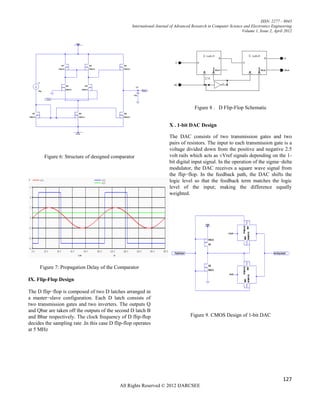
Figure shows the block diagram of a proposed first order
Delta-sigma Converter (Σ-Δ ADC). It consists of
Integrator, a comparator (1 bit ADC), D-latch, 1-bit DAC.
In above circuitry a 1-bit ADC (generally known as a
Comparator), drive it with the output of an integrator, and
feed the integrator with an input differenced with the
output a 1-bit DAC fed from D-latch output.
VI. Circuit Description
The integrator is simple Miller integrator using a large
resistor and small capacitor to minimize layout space. The
values of the resistor and the capacitor decide the time
constant of the integrator .The time constant shouldn’t be
too big. Otherwise, the integrator will go into saturation
status. Op-amp is the core part of the sigma delta
converter .It provides a large open loop gain to integrate
smoothly. The output of integrator feeds to the input of a
comparator referenced to ground to quantize this signal to Figure 4. The Op-amp Design using CMOS [3]
VDD or VSS. This output is then fed to a D flip-flop,
which inserts the necessary delay to clock the circuit. The
output of this is fed into a DAC reference level
adjustment which converts this back to dynamic range of
the input signal. The DAC operates from the Q and Q bar
outputs of the flip-flops. The sum at the input to the
Miller integrator is a negative sum because the DAC
output is negatively referenced. The summing resistance
values are equal to assign an equal weight to both parts in
the integration. The following sections detail the deign
aspects of each circuit component.[4]
VII. Op-amp Design
The operational amplifier that the integrator uses must
have the high gain to effectively carry out a smooth
integration as well as a large enough bandwidth to support
the high frequency sine waves it will be integrating. The Figure 5: The frequency response of op-amp (magnitude
op amp operates at the clock frequency, since the and phase plots)
differences are being integrated over the region of time.
Therefore, the gain bandwidth product of the opamp must VIII. Comparator Design
be greater than one at the clock frequency to effectively
pass the signal. The amplifier used is shown in figure. The The 1- bit Sigma Delta consists of a 1-bit ADC which is
key thing to note to about the amplifier is the frequency composed of a comparator and a D-flip-flop. The design
compensation network which is used to push the high of comparator is similar enough to that of an Op-amp
frequency zero out of the pass band of the opamp. The .The only difference is the use of the compensation
Frequency response of Op-Amp is shown below. The network consists of resistor and capacitor and extra
open loop voltage gain is 10,530V/V, Gain Bandwidth multipliers on a biasing NMOS device. The comparator
(GB) is 5MHz, output resistance is 122.5KΩ, and power does not need the compensation network because its only
dissipation is 0.806 mW. Phase margin for 10pF load is function is to switch from rail to rail. Stability is not
65° and the open loop output voltage swing is needed as it will only slow down the switching speed.
+2.3 to -2.2 V. When a sine wave is input to the circuit, the comparator
switches from positive rail to negative rail. The
propagation delay of the comparator is 5ns.
126
All Rights Reserved © 2012 IJARCSEE](https://image.slidesharecdn.com/43-131-1-pb-120507065549-phpapp01/85/43-131-1-pb-3-320.jpg)
![ISSN: 2277 – 9043
International Journal of Advanced Research in Computer Science and Electronics Engineering
Volume 1, Issue 2, April 2012
XI. Simulation Result of 1-bit Sigma Delta ADC
Authors
The circuit design of first order Sigma -Delta (Σ-Δ ADC)
have been developed and implemented by using 0.18um Anup G. Dakre received the
CMOS technology .The whole First order Sigma-Delta Bachelors of Engineering degree in
ADC system works very well under the following electronics engineering from the
conditions. Nagpur University, India in 2007,
and pursuing his Master in
Input sine wave frequency up to 10 KHz
engineering degree from Pune
University in VIT, Pune (India). He
Clock frequency (D-Latch) 5MHz
is pursuing his post graduation work in Signal Processing
The output signal of converter is a pulse density and VLSI.
waveform .Figure 10 shows the input and output of (Σ-Δ) Contact No:+91-9860287626
ADC modulator.
Figure 10. The Input and Output results of 1-bit Σ-Δ
ADC
XIII. References
[1] “R. Jacob Baker, Harry W. Li and David E. Boyce, CMOS Circuit
Design, Layout, and Simulation. New York, NY: Wiley-IEEE
Press, 1997” chapter 29, pp-790-854
[2] Max W. Hauser, "Principles of Oversampling A/D Conversion,"
Journal Audio EngineeringSocietyVol.39No.1/2, January/February
1991, pp. 3-26
[3] P. E. Allen and D. R. Holberg, CMOS Analog Circuit Design, 2nd
edition, Oxford University Press, 2002.pp.270-280,453-454
[4] “Sigma -Delta Modulator “by Jeremy Ferris, Alfred Blais,
University of Maine.
www.eece.maine.edu/vlsi/Fall_00/SDM_547_Final.pdf
[5] “An Introduction to Delta-Sigma Converters”,
www.beis.de/Elektronik/DeltaSigma/DeltaSigma.html
[6] Walt Kester, Analog-Digital Conversion, Analog Devices, 2004,
ISBN 0-916550-27-3
[7] “ADC Architectures” http://www.springer.com/978-90-481-
8651-8
[8] Ngspice Tool Version 21 by Paolo Nenzi , Holger Vogt
Ngspice home page http://ngspice.sourceforge.net/
128
All Rights Reserved © 2012 IJARCSEE](https://image.slidesharecdn.com/43-131-1-pb-120507065549-phpapp01/85/43-131-1-pb-5-320.jpg)

1) The document describes the design and simulation of a first-order 1-bit sigma-delta analog-to-digital converter (ADC) using Ngspice simulation software. 2) A key component of sigma-delta ADCs is the op-amp, which is used in the integrator stage. The designed op-amp has a high open loop voltage gain and bandwidth suitable for the integrator. 3) The 1-bit sigma-delta ADC was implemented in a 0.18μm CMOS process with a ±2.5V power supply. The circuit was constructed and simulated using Ngspice to verify the design.