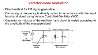
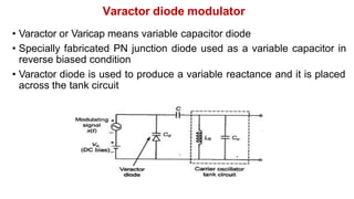
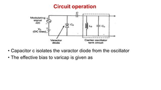
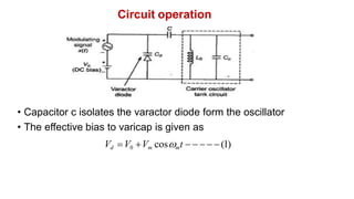
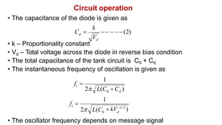
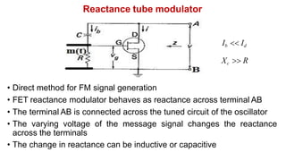
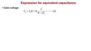
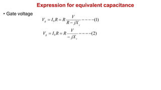
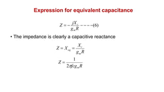
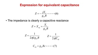
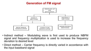
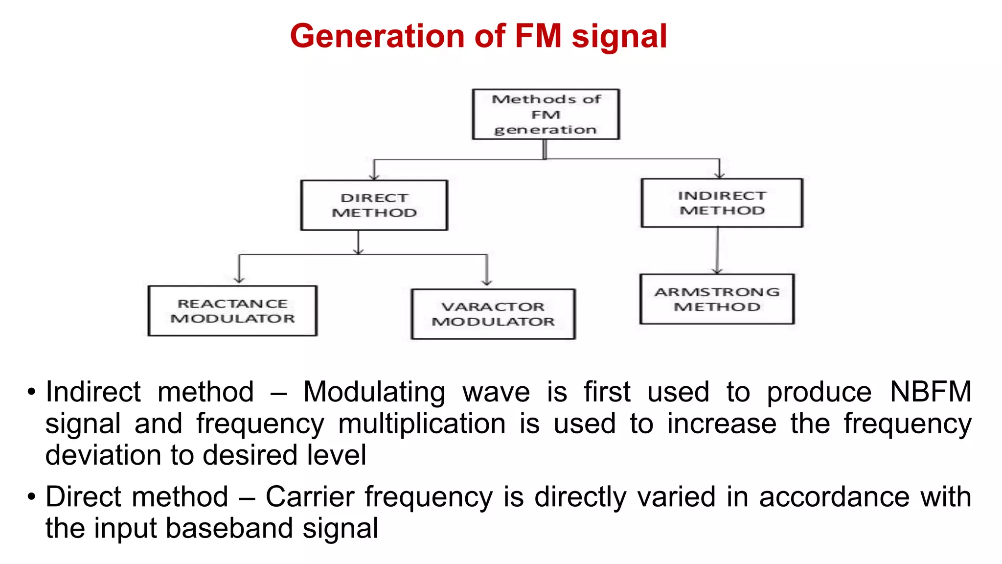
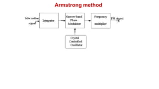
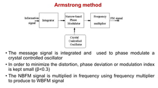
The document discusses various methods of generating FM signals, including the Armstrong method and using a varactor diode or reactance tube modulator. The Armstrong method involves integrating the message signal and using it to phase modulate a crystal oscillator. The output is then multiplied in frequency using a frequency multiplier. Varactor diode and reactance tube modulators directly vary the carrier frequency in accordance with the baseband signal using a voltage-controlled oscillator. The reactance tube modulator behaves as a variable reactance across the oscillator tank circuit, changing the oscillation frequency.
![Armstrong method
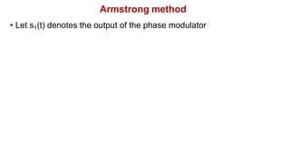
• Let s1(t) denotes the output of the phase modulator
t
s1(t) Ac cos[2f1t 2kf m(t)dt] (1)
0](https://image.slidesharecdn.com/14fmgeneration-230528184440-c68dfffb/85/14-FM_Generation-pdf-5-320.jpg)
![Armstrong method
• Let s1(t) denotes the output of the phase modulator
t
s1(t) Ac cos[2f1t 2kf m(t)dt] (1)
0
• f1 – Frequency of the crystal controlled oscillator
• kf – Frequency sensitivity (constant)
• For a sinusoidal modulating wave, the output s1(t) is given as](https://image.slidesharecdn.com/14fmgeneration-230528184440-c68dfffb/85/14-FM_Generation-pdf-6-320.jpg)
![Armstrong method
• Let s1(t) denotes the output of the phase modulator
t
s1(t) Ac cos[2f1t 2kf m(t)dt] (1)
0
• f1 – Frequency of the crystal controlled oscillator
• kf – Frequency sensitivity (constant)
• For a sinusoidal modulating wave, the output s1(t) is given as
s1(t) Accos[2f1t 1 sin 2fmt] (2)
• The phase modulator output is multiplied ‘n’ times in frequency by
using frequency multiplier to produce the desired WBFM wave](https://image.slidesharecdn.com/14fmgeneration-230528184440-c68dfffb/85/14-FM_Generation-pdf-7-320.jpg)
![Armstrong method
• Let s1(t) denotes the output of the phase modulator
t
s1(t) Ac cos[2f1t 2kf m(t)dt] (1)
0
• f1 – Frequency of the crystal controlled oscillator
• kf – Frequency sensitivity (constant)
• For a sinusoidal modulating wave, the output s1(t) is given as
s1(t) Accos[2f1t 1 sin 2fmt] (2)
• The phase modulator output is multiplied ‘n’ times in frequency by
using frequency multiplier to produce the desired WBFM wave
s(t) Ac cos[2nf1t n1 sin 2fmt] (3)](https://image.slidesharecdn.com/14fmgeneration-230528184440-c68dfffb/85/14-FM_Generation-pdf-8-320.jpg)
![Armstrong method
• In case of sinusoidal modulating wave
s(t) Ac cos[2fct sin 2fmt] (4)
• Frequency multiplier n1 shifts the NBFM to WBFM
• Frequency translator will not change the frequency deviation, it only
shifts the FM signal to either upwards and downwards in the spectrum
• Frequency multiplier n2 is used to increase the Δf and fc
n1
fc nf1](https://image.slidesharecdn.com/14fmgeneration-230528184440-c68dfffb/85/14-FM_Generation-pdf-10-320.jpg)