Essay About SWOT Analysis For Wondermusic, A Non-Profit...
PROJ322 Roberto Weiser Report
1. MINI ELECTRONIC CONGAS FOR MUSIC
PERFORMANCE BY ROBERTO WEISER
A REPORT SUBMITTED TO THE UNIVERSITY OF
PLYMOUTH IN PARTIAL FULFILMENT FOR THE
DEGREE OF BENG (HONS) ELECTRICAL AND
ELECTRONIC ENGINEERING, SPRING 2014
2. 1
ABSTRACT
This report is a technical design guide that covers the whole process involved with the design concepts,
components selection, circuit schematic, PCB layout, software implementation and product design of a
music performance device that imitates the Latin American percussion instrument known as the Conga.
This is followed by a section reviewing the difficulties, and decisions taken to solve the problems
encountered. It also features a cost analysis and a user manual showing how to play the device and
change the samples included, to the own user samples. Finally it reviews the whole project by
suggesting improvements and recommendations for future versions. This report was made to be read
electronically (PDF) as it have links to external websites and videos.
ACKNOWLEDGMENTS
This whole work wouldn’t have been possible without the personal, intellectual and professional support
of certain individuals. Firstly I would like to thanks my parents for giving me all the personal and
financial support to be able to live and study in England, without all their hard work back home it
wouldn’t have been possible for me to have the opportunity to live and learn from this amazing
experience. For this project in particular I want to specially say thank you to my mum, for her full
commitment of finding a craftsman in Venezuela that could build the Mini Congas for me, she asked
half of the country and never stopped until she found the right person. Another person that has been
essential for the development of this project is my friend and ex-colleague Niall Dunican, without his
professional advice and expertise in embedded electronics and programming this project could have
had taken much longer. Lastly I would like to say thank you to the Smeaton electronics lab and
workshop staff for their patience and all the help they offered me across the duration of the project.
3. 2
TABLE OF CONTENTS
Abstract ................................................................................................................................................. 1
Acknowledgments.................................................................................................................................. 1
Glossary ................................................................................................................................................ 3
Introduction............................................................................................................................................ 4
About the Congas and Latin American music ........................................................................................ 4
About music performance devices ......................................................................................................... 6
Project Management.............................................................................................................................. 7
Initial design and considerations............................................................................................................ 8
Design and implementation ................................................................................................................. 27
Modifications, improvements, changes & mistakes.............................................................................. 53
Costs ................................................................................................................................................... 61
Testing................................................................................................................................................. 64
Device User Manual ............................................................................................................................ 67
Conclusions......................................................................................................................................... 68
References .......................................................................................................................................... 71
Appendix.............................................................................................................................................. 74
4. 3
GLOSSARY
These are the abbreviations used in this project which the reader might not be familiar with:
BJT – Bipolar Junction Transistor
CAD – Computer Aided Design
DAC – Digital to Analogue Converter
DCI – Data Converter Interface
DSP – Digital Signal Processor
EQ – Equalizer
ESR – Effective Series Resistance
Hz – Hertz, the unit of frequency
I/O – Input/Output
I2
C – Inter Integrated Circuit
I2
S – Inter-IC Sound
IC – Integrated Circuit
Li-Ion – Lithium Ion
LPF – Low Pass Filter
MCU – Micro Controller Unit
MIDI - Musical Instrument Digital Interface
MIPS – Millions of Instructions per seconds
PCB – Printed Circuit Board
PCM – Pulse Code Modulation
RAM – Random Access Memory
SD – Secure Digital
SMT – Surface Mount Technology
SPI – Serial Peripheral Interface
USB – Universal Serial Bus
Vcc – Power Supply Voltage
5. 4
INTRODUCTION
Music is one of the most beautiful things in life, and it has been around human beings since the
beginning of civilization, the earliest and largest collection of prehistoric musical instruments was found
in China and dates back to between 7000 and 6600 BC [1]. But more impressive than music itself is the
ability to make it, been part of a song can take a person into a state which is hard to describe.
This project came out of a necessity, as a Latin DJ much time is spent waiting for the next song; some
genres such as Salsa and Bachata are completely made of bands. An analogy for the unfamiliar reader
will be to compare a Salsa band with a Rock band, there is a bass, percussion, vocals, pianos and so
on. DJ’s are a relatively new breed of musicians/performers that came to happen as a consequence of
electronic music such as Techno, House and Dubstep. These genres normally have a much defined
4/4 beat which allows the DJ to mix one tune with another. As the reader can imagine, a Rock or Salsa
band doesn’t normally have this beat clearly defined, therefore making it hard for a DJ to mix, simply
because of the nature of the music itself. This is where the necessity of an extra “toy” comes from, DJ’s
are entertainers, and standing idle is never a good thing for a performer, for this reason adding the
ability to play an instrument that can blend well with the music being played can substantially increase
the participation of the DJ. Across Latin America there are Clubs that have already implemented this
idea although they normally have a percussion band alongside the DJ, this project aims to provide the
DJ with a good enough tool to be able to achieve similar results on its own.
The purpose of this project is to create a musical instrument which is normally big and heavy, into a
portable and easy to carry device. This is hoped to be achieved by creating a miniature version of the
actual instrument that can be played with the fingers. Because of the size, sonic properties that define
the Congas will be lost. For this reason an electronic instrument will be designed that can play digital
audio files of the required Conga tones without losing the feel a real drum gives, as much as possible.
Also a low power/renewable energy approach will be adopted.
ABOUT THE CONGAS AND LATIN AMERICAN MUSIC
Much of the culture in Latin America is the result of a blend between European Spanish, black Africans
and native indigenous people, and music is not an exception.
The modern Conga is an adaptation of the African drum which was originally brought by the African
slaves into the Caribbean and the Americas.
The Congas can be heard in most music that comes from the Caribbean/Latin American region and it
has made its way into popular western music as well. It was first popularized in the US during the Salsa
boom in the 1950’s.
Most modern congas have a staved wooden or fiberglass shell, and a screw-tensioned drumhead.
They are usually played in sets of two to four with the fingers and palms of the hand. Typical congas
stand approximately 75 centimeters (30 in) from the bottom of the shell to the head. The drums may be
played while seated. Alternatively, the drums may be mounted on a rack or stand to permit the player to
play while standing [2]. Figure 1 shows a standard Conga setup:
6. 5
FIGURE 1: STANDARD CONGAS SETUP
STROKES
There are five basic strokes [2]:
Open tone (tono abierto): played with the four fingers near the rim of the head, producing a clear
resonant tone with a distinct pitch.
Muffled or mute tone (tono ahogado): like the open tone, is made by striking the drum with the
four fingers, but holding the fingers against the head to muffle the tone.
Bass tone (tono bajo): played with the full palm on the head. It produces a low muted sound.
Slap tone (tono seco): the most difficult technique producing a loud clear "popping" sound
(when played at fast and short intervals is called floreo, played to instill emotion in the dancer).
Touch tone (toque de punta): as implied by the name, this tone is produced by just touching the
fingers or heel of the palm to the drum head. It is possible to alternate a touch of the palm with a
touch of the fingers in a maneuver called heel-toe (manoteo), which can be used to produce the
conga equivalent of drumrolls.
If the reader is interested in watching a demo of the Congas being played please follow the YouTube
link [3]
7. 6
THE CONGAS IN DIFFERENT MUSICAL GENRES
Congas are one of the many percussion instruments in a typical Latin American/Caribbean band. In
combination with the Bongos they play a very important role as they add a distinctive and important
component in the music. Since it is a percussion instrument and doesn’t have defined notes such as a
piano, the Conga can be implemented in countless styles as a background instrument. In the Latin
American music world it can normally be heard in genres such as Salsa, Bachata and Merengue where
it normally plays an important role as one of the main percussion instruments.
Example of the Congas in Salsa: YouTube link [4]
ABOUT MUSIC PERFORMANCE DEVICES
For the last 5 years there has been a change in the market where DJing if shifting from traditional vinyl
disc and CD players into controllers, which are devices that normally connect to a computer via USB
and control a software using MIDI commands. This controllers range from traditional looking devices
that imitate the original DJ setup which is composed by a 2 channels mixer, EQ control, pitch control, a
disc plate and faders, to drum pads, synthesizers and touch sensitive devices, there is even the
development of controllers which work with iPads. All the devices mentioned before share the same
characteristics as the Mini Congas: they are all small portable device and have the purpose of giving
more tools to the DJ in order to make a better performance.
Some of the devices that have the closest similarity to this project are the drum pads, which are
essentially the same idea as the Mini Congas; they played assigned samples when they are hit,
however they are not stand alone and require a software and to be connected to the computer. An
example of such devices is the Akai LPD8 which can be bought for the modest price of £32.00 and
seen in Figure 2 [5]:
FIGURE 2: AKAI LPD8
Another device that is quite similar to the proposed in this project is the Acoustic Solutions CDD 302
Mini. This is a 4 pad electronic drum kit, however it is not as portable for a DJ to carry. The device can
be appreciated in Figure 3 and acquired by a price of £50.00 [6].
8. 7
FIGURE 3: ACOUSTIC SOLUTIONS CDD 302 MINI
The Mini Electronic Congas will aim to achieve a combination of the characteristics offered by the
previous two devices:
Keep the quality and feel/response of real drums
The device should be stand alone and not dependent of external software and power source
PROJECT MANAGEMENT
This section aims to show how the project development stages will be distributed throughout the
academic year
The project consists in 4 main stages:
1. Hardware design
2. Software design
3. Debugging and testing
4. Report writing
To administrate these task and its subsequent subtasks a Gantt chart was used. The Gantt chart can
be found in the Appendix.
Although the Gantt chart was a rough guide to keep track of timing, it was of clear importance as it
helped to manage and keep track of the work done.
9. 8
INITIAL DESIGN AND CONSIDERATIONS
In this section general ideas of how to design the Mini Congas will be shown, also the specifications
and requirements will be laid down. This is followed by specifying the type of components required and
the justification of why they were selected.
Concept approach
Every idea starts in the head, the hard part is to take the idea in the head and make it into something
tangible.
OBJECTIVES
To have a stand-alone device capable of reproducing, adjust gain and mix digital audio file(s) when the
user hits one of the drums with the least latency possible and maximum battery life, and able to
recharge it. Also make it the smallest size possible to increase portability.
SPECIFICATIONS
The following is a technical list of the required specs for the project
1. Device should be small and light enough to be carried and fitted in tight spaces
2. Device should aesthetically look like a Conga and feel like a drum
3. Device should run on battery for at least 5 hours, therefore consuming the least power possible
4. Battery should be able to be recharged via USB or a solar panel
5. Latency should be less than 100mS as it is the minimum latency perceived by a human [7]
6. Device should have the highest audio quality possible
7. User should be able to change the samples stored in the device
8. The device should at least have 3 different volume levels which should adjust according to the
strength of the hit to the drum by the user
9. The device should be able to mix digital audio files in real time
10. Device should have an audio output that can be connected to an external mixer or amplifier
11. Device should have an ON/OFF switch
12. The device should be in a box that can be easily opened in order to see the circuit
13. There must be a light that indicates the device is ON and another one to indicate that is
charging
REQUIREMENTS
In order to meet the specifications the following will be required:
1. A small object that looks like a Conga
2. Sensors to go inside
3. A battery
4. USB port
5. External solar panel
6. A fast MCU that can deal with mathematical operations
7. A high quality DAC
8. A system to detect and assign different volumes to the drums hit
9. External memory that can be easily accessed by the user
10. 9
Engineering approach to the concept
Using the previous specifications and requirements a solution was developed, this is best expressed in
diagrams that will be explained in a later section.
GENERAL HARWARE BLOCK DIAGRAM
MCU
Sensor
Buffer/Amp
External
Memory
DAC
LPF
LPF
Battery
Switch
Solar Panel
Programmer
Voltage
Regulator
USB Power
Battery Charger
IC
Sensor
Buffer/Amp
Sensor
Buffer/Amp
Sensor
Buffer/Amp
Sensor
Buffer/Amp
Sensor
Buffer/Amp
Comparator Array
Indicator
Indicator
Crystal
Serial
Serial
LOUT
ROUT
3x lines
3x lines
3x lines
3x lines
3x lines
3X lines
FIGURE 4: HARDWARE BLOCK DIAGRAM
11. 10
GENERAL SOFTWARE FLOWCHART
FIGURE 5: GENERAL SOFTWARE FLOWCHART
Start
Declare global variables
Configure MCU and
peripherals
External Interrupt?
Poll flags
Enter Idle mode and
wait until interrupt
happens
No
flag is high?
No
Set Input flags if
interrupt has been
triggered
Yes
End of interrupt
Load buffer with
respective file from
external memory
Apply gain accordingly
to digital data
Send data to digital
mixer
Mix data and send to
DAC
Return
Yes
Another interrupt flag is
high?
No
Yes
12. 11
INITIAL MECHANICAL DRAFTS FOR PARTS
The following photo is a rough design taken from the Log Book which shows the initial dimensions and
how the board will be spread.
FIGURE 6: INITIAL PRODUCT DESIGN
Decisions and designs about the Mini Conga will be explained in detail in a later section.
13. 12
Getting into detail with the electronics
This section explains first why a particular type of component or device is required for the design with a
short explanation of how it works and how it will affect the final design. Then different communication
interfaces are researched to find out which might be the best for the proposed design. Finally the
components selection is discussed by comparing different options where appropriate and explaining
why they were chosen.
ENGINEERING SOLUTIONS TO MEET THE SPECIFICATIONS
Battery
As mentioned above, the device will run on battery and the battery needs to be able to be recharged.
Also because of the low power approach it needs to be a low voltage battery. Another consideration is
the current capacity. Since we need the device to be able to stay on for 5 hours, then, on the
assumption that the device won’t consume more than 100mAh, a battery is required that have a
capacity of at least 500mAh. The battery also needs to be recharged through a 5V source with a max
current of 500mA according to USB power specifications [8].
The following table compares different types of battery materials [9]:
TABLE 1: COMPARISSON OF DIFFERENT BATTERY MATERIALS
Parameter NiCd NiMH Lead
Acid
Li-ion Li-ion
polymer
Reusable
Alkaline
Gravimetric Energy Density(Wh/kg) 45-80 60-120 30-50 110-160 100-130 80 (initial)
Internal Resistance
(includes peripheral circuits) in mΩ
100 to 200
6V pack
200 to 300
6V pack
<100
12V pack
150 to 250
7.2V pack
200 to 300
7.2V pack
200 to 2000
6V pack
Cycle Life (to 80% of initial capacity) 1500 300 to 500 200 to
300
500 to
1000
300 to
500
50
(to 50%)
Fast Charge Time 1h typical 2-4h 8-16h 2-4h 2-4h 2-3h
Overcharge Tolerance moderate Low high very low low moderate
Self-discharge / Month (room
temperature)
20% 30% 5% 10% ~10% 0.3%
Cell Voltage(nominal) 1.25V 1.25V 2V 3.6V 3.6V 1.5V
Load Current
- peak
- best result
20C
1C
5C
0.5C or
lower
5C
0.2C
>2C
1C or
lower
>2C
1C or lower
0.5C
0.2C or
lower
Operating Temperature(discharge
only)
-40 to
60°C
-20 to
60°C
-20 to
60°C
-20 to
60°C
0 to
60°C
0 to
65°C
Maintenance Requirement 30 to
60 days
60 to
90 days
3 to 6
months
not req. not req. not req.
Typical Battery Cost
(US$, reference only)
$50
(7.2V)
$60
(7.2V)
$25
(6V)
$100
(7.2V)
$100
(7.2V)
$5
(9V)
Cost per Cycle(US$) $0.04 $0.12 $0.10 $0.14 $0.29
Commercial use since 1950 1990 1970 1991 1999
14. 13
Battery charging
A battery needs to be charged according to its voltage, current capacity and material used. Connecting
the battery straight to the power source could damage the battery and considerably decrease its life
cycle. For this reason a circuit must be designed which can manage the battery charging. Alternatively
a battery charger IC can be a viable option.
There are different ways of charging a battery. Each different method is used for a different type of
material. A common parameter in battery charging is the C rate, which is a way of expressing how
much current is being used in comparison with the rated current capacity of the battery. For example: if
a battery is charged at 0.3C for a 600mAh battery, then the charger will constantly output 180mA.
𝐼𝑜𝑢𝑡 = 600𝑚𝐴ℎ × 0.3 = 180𝑚𝐴ℎ
Table 2 [10] compares different charging methods with different battery types and C rates.
Type Chemistry C-rate Time Temperatures Charge termination
Slow
charger
NiCd
Lead acid
0.1C 14h 0ºC to 45ºC
(32ºF to
113ºF)
Continuous low charge or fixed timer. Subject to
overcharge. Remove battery when charged.
Rapid
charger
NiCd, NiMH,
Li-ion
0.3-
0.5C
3-6h 10ºC to 45ºC
(50ºF to
113ºF)
Senses battery by voltage, current, temperature
and time-out timer.
Fast
charger
NiCd, NiMH,
Li-ion
1C 1h+ 10ºC to 45ºC
(50ºF to
113ºF)
Same as a rapid charger with faster service.
Ultra-fast
charger
Li-ion, NiCd,
NiMH
1-10C 10-60
minutes
10ºC to 45ºC
(50ºF to
113ºF)
Applies ultra-fast charge to 70% SoC; limited to
specialty batteries.
TABLE 2: COMPARISSON BETWEEN DIFFERENT CHARGING METHODS
Power Management
Even though the power source is a DC source, it still needs to be regulated in order to reduce ripple
caused by spurious current bursts and isolate it from the rest of the electronics in the circuit. A typical
approach is to use a voltage regulator, which produces a steady voltage source, capable of dealing with
supply ripples. Voltage regulators are mainly divided into two categories:
Linear
A linear regulator operates by using a voltage-controlled current source to force a fixed voltage to
appear at the regulator output terminal. The control circuitry must monitor (sense) the output voltage,
and adjust the current source (as required by the load) to hold the output voltage at the desired value
[11].
Linear regulators subdivide into Low Drop Out (LDO) and Standard. The main difference between both
is dropout voltage, which is defined as the minimum voltage drop required across the regulator to
maintain output voltage regulation. A critical point to be considered is that the linear regulator that
operates with the smallest voltage across it dissipates the least internal power and has the highest
efficiency. The LDO requires the least voltage across it, while the Standard regulator requires the most
[11].
15. 14
Switching
A switching regulator converts the DC input voltage to a switched voltage applied to a power MOSFET
or BJT switch. The filtered power switch output voltage is fed back to a circuit that controls the power
switch on and off times so that the output voltage remains constant regardless of input voltage or load
current changes [12]. Typical topologies for switching regulators include: the buck, which converts a
higher input voltage into a lower output voltage and a boost which converts a lower input voltage into a
higher output voltage.
Regulators comparison
Table 3 [13] compares Linear with Switching regulators:
Regulator Linear Switching
Function Only steps down; input voltage must be
greater than output
Steps up, steps down, or inverts
Efficiency Low to medium, but actual battery life
depends on load current and battery
voltage over time; high if VIN -
VOUT difference is small
High, except at very low load currents (µA), where
switch-mode quiescent current (IQ) is usually higher
Waste Heat High, if average load and/or input/output
voltage difference are high
Low, as components usually run cool for power
levels below 10W
Complexity Low, which usually requires only the
regulator and low-value bypass
capacitors
Medium to high, which usually requires inductor,
diode, and filter caps in addition to the IC; for high-
power circuits, external FETs are needed
Size Small to medium in portable designs, but
may be larger if heatsinking is needed
Larger than linear at low power, but smaller at
power levels for which linear requires a heat sink
Total Cost Low Medium to high, largely due to external
components
Ripple/Noise Low; no ripple, low noise, better noise
rejection
Medium to high, due to ripple at switching rate
TABLE 3: LINEAR VS SWITCHING REGULATORS
Microcontroller
In order to control, process, easily change parameters of the design on demand and keep the design
tidy and relatively low complexity, it is unpractical to approach a solution using purely discrete analogue
and digital components. For this reason, a natural choice is the use of a microcontroller. A
microcontroller is basically a computer shrinked to a chip. It contains a CPU, memory, I/O pins and
peripherals, all in a single package [14]. The following section will aim to explore and explain where
appropriate, the features that are required for the proposed design.
Types or models
There are many microcontrollers’ manufacturers and architectures in the market, some that are most
common in the market and the “student and hobbyist” sector are:
PIC from Microchip
AVR from Atmel
8051 from Intel
ARM from different manufacturers
16. 15
Each different type has its own advantages and disadvantages but at the same time they can all be
very similar as well. For this reason, different models will be considered at the time of selecting a MCU
in a later section.
Peripherals
According to the Hardware Block Diagram (Figure 4), the following peripherals are required in the MCU
Two serial interfaces to communicate with external memory and DAC (serial interfaces will be
discussed in a later section)
A timer might be necessary for time sensitive subroutines
I/O Pins
From the Hardware Block diagram (Figure 4) it can be seen that a number of I/O pins are required.
There are 3 lines from every comparator array, and there are six of those, that makes a total of 18
required pins. Also some of the serial peripherals might require an extra I/O pin, for that reason the
minimum number required will be 20. Also the comparator pins are required to work as external
interrupts, this means a MCU with a minimum number of 18 external interrupts will be necessary.
CPU speed
Because of the mathematical operations, in particular the digital mixing, a fairly quick CPU will be
required. The CPU will need to fetch data from the external memory and do the mathematical
operations in less time than the sample rate of the audio file, which is normally 44.1 KHz or 22.67 uS.
Determining theoretically how long the processor will take to do the processes mentioned above is
unrealistic as it cannot be accurately determined until the code has been written and optimized. For this
reason the aim will be to acquire a MCU that can work at high CPU speeds.
Crystal
Microcontrollers normally have an inbuilt oscillator, but usually it is not a very fast one. Therefore an
external oscillator is required which is normally achieved by using a crystal that connects directly to the
microcontroller pins that have an internal oscillator circuit. Standard values of crystals are normally
between 8-16MHz, which is not fast enough for performance applications. Most microcontrollers
employ a technique called Phase Locked Loop (PLL), this is a feedback system combining a voltage
controlled oscillator (VCO) and a phase comparator so connected that the oscillator maintains a
constant phase angle relative to a reference signal. Phase-locked loops can be used to generate stable
output high frequency signals from a fixed low-frequency signal [15]. Therefore PLL is a necessary
feature in this design in order to achieve high clock speeds from a cheaper and slower crystal.
Memory
The memory in microcontrollers is specially designed to hold the program or firmware. For this reason
is normally small, fast, and reprogrammable. Since the audio samples are relatively big compared to
internal memory, this will not be a critical parameter as it will only be used to store the program.
Another type of memory included in the microcontroller is RAM memory. This parameter is more
important for the proposed design as the device needs to be able to hold buffers in memory which can
be relatively big. For this reason a MCU with a substantial amount of RAM is desirable.
17. 16
DSP features
Because of the mathematical operations involved it will be beneficial to have DSP capabilities in the
microcontroller, this way the time taken to perform the operations could be substantially reduced.
However it might not be necessary if the CPU speed is fast enough.
Programming interface
In order to program the microcontroller a programmer/debugger is necessary, this is normally found on
the manufacturer of the MCU or with third parties. The main aspect when looking for a programmer is
that it can interface with the MCU with the less hassle possible. This means by avoiding complicated
connections or required pre-programming.
Sensors
The aim of the sensors is to provide the microcontroller with a reference or a signal in the form of a
voltage that a drum has been hit.
The first obvious approach is to have a simple push switch that will go high when the user hits the
drum. This could be an acceptable approach, however it will not replicate realistically the feel of real
drums. Also with time and constant hitting the mechanical parts of the switch could break.
Another option is to use a piezoelectric sensor, which is normally used in electronic drums [16] [17].
The piezoelectric sensor is used for flex, touch, vibration and shock measurement. Its basic principal, at
the risk of oversimplification, is as follows: whenever a structure moves, it experiences acceleration. A
piezoelectric shock sensor, in turn, can generate a charge when physically accelerated [18]. This
means that when the sensor is hit it can generate a voltage proportional to the strength of the hit and
replicating its natural oscillation and decay.
Sensors to MCU interface
If a piezoelectric sensor is to be used then it cannot be connected straight to an I/O pin for this
particular application. This is because the I/O pin will only read as high or low, meaning that there won’t
be a way to tell the MCU if the impact signal was of low, medium, or high voltage, therefore there is no
way to set the corresponding gain of the sample. There are two approaches to resolve this issue:
Using an Analogue to Digital Converter (ADC)
Most microcontrollers have one or more inbuilt ADC’s. By feeding the signal from the piezoelectric
sensor to the ADC, the software can then compare the actual signal with the ADC range and set a
determined gain value. For example, if an 8 bit ADC is used then it will have 28
or 256 different possible
levels, then when the program reads the signal it will look for the highest peak and from there give a
gain value. So if the highest peak is at 167 that means that 0.65 of the ADC range was used (256/167)
therefore it will set the gain of the sample at 0.65 or 65%.
Using a comparator array
Another way to approach the problem is to use a comparator array as expressed in the Hardware Block
Diagram (Figure 4). The way this work is by using 3 comparators per sensor, each comparator will be
set at a different voltage level, for example: 1, 2 and 3 Volts. Then when the sensor is hit, it will produce
a voltage that depending on the strength of the hit, it will trigger one, two or all comparators. These
comparators will be connected to the I/O pins in the MCU, and then the program can read the inputs
and detect the level of gain. For example: when a soft hit happens it will trigger only one comparator
18. 17
therefore the MCU will see in its inputs a 001 (each digit is a separate comparator). This then means
that the lowest gain should be applied to the sample so 0.35. Opposite scenario, the drum is hit very
strong and all comparators trigger, showing a 111 in the inputs, therefore the gain applied to the file will
be 1.
External memory
As required by the specifications, external memory will store the samples, and it should be accessible
by the user in order for him/her to change the samples if desired. Serial interfaced types of memories
will only be considered since they have a lower circuit complexity and power consumption. Two
different types of memory will be reviewed for this project:
EEPROM
Electrically Erasable Programmable ROM, EEPROMs are a type of non-volatile memory that allows
data to be written to each address via electric signals. Unlike bytes in most other kinds of non-volatile
memory, individual bytes in a traditional EEPROM can be independently read, erased, and re-written
[19].
Flash
Flash memory is an electronic non-volatile storage medium that can be electrically erased and
reprogrammed. There are two main types of flash memory, which are named after
the NAND and NOR logic gates. The internal characteristics of the individual flash memory cells exhibit
characteristics similar to those of the corresponding gates.
Whereas EPROMs had to be completely erased before being rewritten, NAND type flash memory may
be written and read in blocks (or pages) which are generally much smaller than the entire device [20].
Types of Flash memory
Discrete Flash NAND IC
Flash NAND IC’s can be found in small packages of 8-pin, with adequate storage capacity. The main
advantage of using a discrete IC is that it can reach speeds of up to 400 MB/s interfacing via SPI. It
also features a low current consumption of a max of 50mA over 3.3V [21].
SD Card
Secure Digital cards is a form of flash NAND, in a more complete package. It incorporates the memory
with a controller in a single package. Making the final device more flexible and convenient at the
expense of speed and power consumption. SD cards are divided into different categories depending on
its capacity and speed. Capacity varies from 2 GB to more than 32 GB and speed from 2 MB/s to 312
MB/s for top performance cards. SD Cards also feature a SPI interface mode. Power consumption can
be up to 100mA over 3.3V with inrush currents of the order of 200mA [22].
DAC
A Digital to Analogue Converter, is responsible for converting the digital samples of the audio file, into a
voltage waveform, this is done by outputting a voltage at the right amplitude and at the right time,
because this process is done so fast (at least every 25uS) it seems like a constant waveform to the
human perception. There are different types of DAC’s, such as Delta Sigma and Ladder, which their
19. 18
main difference is the way they output the amplitude of the waveform while the timing remains the
same as it is done by an external clock [23].
Following the specification of achieving the highest audio quality possible, the integrated DAC that
normally an MCU has, will not be used. Therefore an external DAC with a serial interface will be
required.
The main specs desired in the DAC for this particular design are:
Resolution of at least 16-bit
Sampling rate of at least 44.1 KHz
Extra features such as up sampling and internal anti-aliasing filter
Minimum number of pins and small package
Serial interface
Post DAC Low-pass filter
A low pass filter after the DAC will be necessary in order to filter any high frequency harmonics created
by the DAC. These harmonics are called imaging and are generated when the DAC “waits” for the next
amplitude of the next sample, this is an inherent property of all sampled systems and generates a “stair
case” waveform as seen in Figure 7 [24]:
FIGURE 7: EFFECTS OF ALIASING
20. 19
Typical low pass filters with a corner frequency of 20 KHz (upper limit of human hearing) can be used.
This includes passive filters using resistors and capacitors or active filters using operational amplifiers.
Filters will normally have a Butterworth response as it has the less ripple in the band pass area.
CHOOSING COMMUNICATION INTERFACES
Note that this technical report is only concerned in using the available technologies and finding
information already available rather than research as a main goal. For this reason explanations of the
communication interfaces has been directly taken from outside sources and are referenced accordingly.
Serial Peripheral Interface (SPI)
SPI was first introduced by Motorola in 1979 and it has become one of the most popular ways to
interface peripherals in embedded systems.
SPI is a single-master communication protocol and it requires a minimum of 4 data lines. This means
that one central device initiates all the communications with the slaves. When the SPI master wishes to
send data to a slave and/or request information from it, it selects a slave by pulling the corresponding
CS line low and it activates the clock signal at a clock frequency usable by the master and the slave.
The master generates information onto the Master Out-Slave In (MOSI) line while it samples the Master
In-Slave Out (MISO) line. SPI bus speed is limited by the controller used rather than the protocol. [25]
Inter-Integrated Circuit (I2C)
I2
C was developed in 1982 by Philips and its original purpose was to provide an easy way to connect a
CPU to peripheral chips in a TV set.
I²C is a multi-master protocol that uses 2 signal lines. The two I²C signals are called ‘serial data’ (SDA)
and ‘serial clock’ (SCL). There is no need of chip select (slave select) or arbitration logic. Virtually any
number of slaves and any number of masters can be connected onto these 2 signal lines. The data rate
has to be chosen between 100 kbps, 400 kbps and 3.4 Mbps, respectively called standard mode, fast
mode and high speed mode. [25]
Inter-IC Sound (I2S)
Developed by Philips, this less-heard serial interface was specially designed to interface digital audio
serially between IC’s.
The bus has only to handle audio data, while the other signals, such as sub-coding and control, are
transferred separately. To minimize the number of pins required and to keep wiring simple, a 3-line
serial bus is used consisting of a line for two time-multiplexed data channels (DIN), a word select line
(LRCLK) and a clock line (BCLK). Since the transmitter and receiver have the same clock signal for
data transmission, the transmitter as the master, has to generate the bit clock, word-select signal and
data. [26]
21. 20
COMPONENTS SELECTION
In this section the actual components used in the circuit will be selected according to the design
specifications. Comparisons between different alternatives will be made where appropriate. Please note
as well that all datasheets can be found at the Appendix
General criteria
The following are features and characteristics that all the devices are required to have:
Audio Quality
Because audio quality is of foremost importance, device selection needs to always take into account
this parameter. Extra allowance on price will be allocated if it delivers a better audio performance.
Size
This project needs to be physically small. For this reason components in the format of SMT and
minimum number of pins will be required.
Power
Another parameter of high importance is the power usage each component has. Because the design
aims to extend the battery life as much as possible, components with low power consumption will only
be considered.
Cost
The project budget is of £100. Low costs components will be selected as long as they do not interfere
with the parameters mentioned above.
Battery
The battery type selected for the design was Li-Ion for the following reasons as seen in Table 1
Fast charge time (2 to 4hours)
o This is required from the specifications
Cell Voltage (3.6V)
o This is beneficial for the tidiness of the design as only one battery will be necessary and
it is also close to 3.3V
Maintenance required (none)
o This is very beneficial as the user will not need to change the battery unless it totally
breaks
To select a Li-Ion battery different manufacturers were looked however most of them did not offer many
options below the 1Ah range. An adequate battery was found from the manufacturer EEMB Battery with
the following specifications:
Nominal capacity: 550mAh
Nominal Voltage: 3.7V
Charging method: Constant current/Constant voltage
22. 21
Battery charging
To charge the battery it was decided to use an IC instead of creating a circuit with discrete components.
This way it will save space and design time. Because of the type of battery selected, an IC specially
designed to recharge Li- Ion batteries will be necessary. It also needs to be able to charge the battery
on a CC/CV mode at 4.2V and be able to flash an LED to indicate the user when charging is complete.
The IC MCP73831” Miniature Single-Cell, Fully Integrated Li-Ion, Li-Polymer Charge Management
Controller” from Microchip is a battery charger IC designed to charge a Li- Ion battery through USB
power, and it was selected as it satisfied all the requirements at a low cost.
Solar Panel
The required solar panel ideally should behave on the same way as the USB power input. From the
MCP73831 it was found that the minimum input voltage must be 3.75V while the maximum is 7V. Also
the charging current can be set with a resistor (more on this in the circuit design section).
A module with flexible silicon film was selected from the UK manufacturer Select Solar. This module
featured an open circuit voltage of 6.8V and a short circuit current of 125mA at 100% Sun. With a
working voltage and current of 4.8V and 100mA respectively advertised. The implementation of a
Maximum Power Point Tracker circuit was thought however it was discarded as it will increase the
complexity of the board and it will not be of much benefit because of the small power output from the
panel.
Power Management and circuit protection
To regulate the battery voltage a 3.3V linear regulator was selected for the following reasons:
Low circuit complexity
Does not introduce switching noise in the power supply
Voltage drop will only be 0.4V so not much power will be wasted in the form of heat
(0.4x0.1=0.4 Watts approx.)
The TC1262 from Microchip was selected for the following features:
Very Low Dropout Voltage
High accuracy
Over current and over temperature protection
Small PCB package
Designed specifically for battery operated systems
Also a 250mA, very fast acting fuse from Littelfuse was selected for extra circuit protection.
Microcontroller
Features required in the microcontroller will be summarized for simplicity:
1. Popular and well-resourced manufacturer
2. Two SPI peripherals
3. One I2
C peripheral
4. One I2
S peripheral
23. 22
5. A timer
6. 20 I/O pins of which 18 are interrupt controlled
7. Fast CPU speed support
8. PLL support
9. Substantial amount of RAM
10. DSP features
11. Easy and practical programming interface
12. Low power
13. Lowest pin count
Many microcontrollers in the market can meet all those requirements, therefore microcontroller
selection is stripped down to the preference of the implementer/programmer. For this reason it was
decided to select a MCU from Microchip as the designer had the most experience working with PIC’s
above all other options.
The microcontroller selected was the 16-bit digital signal controller dsPIC33FJ128GP706A for the
following reasons:
PIC microcontrollers are very popular and there are many forums and code examples available
in the web to support programmers
Two SPI modules
Two I2
C modules
One I2
S module
Up to nine 16-bit timers
53 I/O pins with external interrupt support
CPU speed up to 40 MIPS with low jitter PLL support
16 KB of RAM
DSP features included (two 40-bit accumulators)
Dedicated software (MPLAB X) and programmer (REAL ICE) available in the Smeaton Lab
Low power modes including Idle and Sleep
TQFP 64-pin PCB package
Crystal
To choose a crystal it was simply selected a crystal with an even number in between 10 and 20 MHz so
it can be easily scaled by the PLL. A 16 MHz quartz crystal was selected.
Sensors
A piezoelectric sensor was selected over the push button for its robustness and its natural imitation of a
drum hit in the form of a voltage.
The ABT-441-RC from Multicomp was selected as it has an adequate size that fits the mechanical
dimensions of the project.
Sensors to MCU interface
Using an ADC gives extra accuracy and lower circuit complexity as there is no need of external
components since the ADC will be part of the MCU. However it comes with more challenges at the time
24. 23
of programing and it introduces delay as the MCU will have to sample the signal at regular intervals,
possibly delaying the whole process too much, therefore not meeting the design specifications. Also it
will require a total of 6 ADC’s. For these reasons it was decided to use a comparator array instead.
Before the comparator array the signal needs to be conditioned first by a buffer/amplifier. For this the
MCP601 operational amplifier from Microchip was selected for the following reasons:
Single supply: 2.7V to 6V
Low quiescent current (230uA)
Single PCB package
CMOS high impedance input as required to interface piezoelectric sensors [27]
The following step is to choose the comparator. Note a change in the design: because a comparator
with 3 inputs could not be found, the design was changed to only having two different gain levels. This
decision was taken as it will reduce PCB design complexity and lower the cost of the final product.
The dual input comparator LM2903 from ST was chosen as it featured a single supply operation (2V
min) and low power consumption (0.4mA).
External memory
For the selection of external memory, it was only considered flash NAND, as it is normally used in
applications where memory needs to be overwritten, while EEPROM can be found in applications
where the memory does not change, such as in computer BIOS.
From the flash NAND options it was selected the SD card over the flash NAND IC for the following
reasons:
Practicality: the SD card can be easily removed and files changed by the user
Microchip features an SD library with the aim of making the interface of SD card with the PIC as
seamless as possible
SD cards does not require pre-programming
DAC
The selected DAC was the WM8727 from Wolfson microelectronics. This is a high performance DAC
that supports 16-24-bit I2
S digital audio interface. It supports sampling rates up to 192 KHz, has internal
low pass filters and it comes in a small 8-pin PCB package.
Low-pass filter
Because the DAC has an internal low pass filter, a simple single pole RC filter will be used. However
the components selected will have in mind audio quality. For the resistor, a metal film 0.25W will be
selected as it introduces less noise in comparison with thick film 0603 resistors. For the capacitor, a
metal film polypropylene will be used as it has low loss and good capacitance stability. Capacitors from
the German manufacturer WIMA were selected as they are highly regarded in the audiophile
community.
25. 24
Oscillator
The DAC requires an external oscillator to drive the master clock. An oscillator was designed using a
crystal and an unbuffered inverter configuration (more info in the circuit design section). The
NL27WZ04DTT1G dual inverter from On Semiconductor was selected.
Connectors
The board will require connectors to interface with external cables and components.
Audio Outputs: standard phono jack connectors will be used
USB input: a micro USB connector will be used
Solar panel in: for this a phono jack will be used as well as it can be easily connected from
outside
SD Card slot: a microSD card slot will be selected to hold the card and connect it to the PCB
tracks
Generic connectors: to connect the sensors and ON/OFF switch, generic Molex connector will
be used
Getting into detail with software
This section is concerned in exploring and finding ways to meet the specifications from a software and
programming perspective.
PROGRAMMING LANGUAGE, ENVIRONMENT AND AUDIO FORMAT DECISIONS
The choose of programing language will be C and the software used for writing the code, compiling it,
and debugging it will be Microchip MPLAB X. Also it was decided that the format of the audio file will be
in RAW with a bit depth of 16-bit and a sampling rate of 48 KHz. This decision was taken because
RAW files are pure PCM code without any headers files that are not necessary for the application. The
bit depth set to 16-bit is because the PIC peripheral that sends the audio data only supports a max of
16-bit per transmit buffer and 48 KHz were chosen as it is good quality and it will take less time for the
PIC to fetch the data from the SD card since there is less samples per second, compared to 96 KHz for
example.
SPECIAL SUBROUTINES REQUIRED
The following are required subroutines especially for the type of application the design involves.
Reading data from SD card
Reading files from the SD card through SPI is a complex process that will take an enormous amount of
time to code for a beginner – intermediate programmer. Fortunately, Microchip has already developed a
library where the programmer can easily implement code to read, write and modify files in the SD card.
These libraries will be used and configured accordingly for the application.
Buffering data
Data needs to be fetched intelligently from the SD card and stored in a buffer which in turn will send the
data to the I2
S peripheral. However this peripheral will only send data every 20.83 uS, and is
impractical to wait for the buffer to empty and do nothing for that period of time. For that reason, a
circular buffer in combination with the peripheral interrupt will be implemented. This way the buffer will
be continually filled and the peripheral interrupt will only trigger every 20.83 uS and send the oldest
26. 25
data in the buffer. A circular or ring buffer is a general purpose data structure that implements a cyclic
first-in-first-out (FIFO) queue, convenient for buffering data streams or other types of sequential
communications where newer data can be allowed to overwrite older [28]. Figure 8 is a useful graphical
representation of a circular buffer:
FIGURE 8: CIRCULAR BUFFER GRAPHICAL REPRESENTATION
In addition to the memory buffer itself, the structure maintains [28]:
Two offsets — one for reading, and one for writing to the queue;
The buffer’s current capacity (the maximum number of elements it can hold)
A bytes count holding the number of elements currently in the buffer.
Applying different gains and mixing signals digitally
The method describing in how to choose which gain needs to be applied to the data has been
described in an earlier section.
To apply the gain, the sample will be multiplied by half its original value so:
𝑆𝑎𝑚𝑝𝑙𝑒_1 = 𝑆𝑎𝑚𝑝𝑙𝑒_1 × 0.5
However to avoid floating point arithmetic the operation will divide the sample by two instead:
27. 26
𝑆𝑎𝑚𝑝𝑙𝑒_1 =
𝑆𝑎𝑚𝑝𝑙𝑒_1
2
To mix the samples, Equation 2 will be used [29] :
𝑍 = 𝐴 + 𝐵 −
𝐴 × 𝐵
2 𝑛
EQUATION 1: DIGITAL MIXER OPERATION
Where A and B are the samples and n is the bit depth of the samples. The purpose of this equation is to
mix the samples avoiding any clipping or loss of information and maintaining the maximum dynamic range
available. A full explanation of the method can be found in the referenced website.
Getting into detail with mechanical parts
The following section explains decision made regarding the mechanical parts and the guidelines that
will be used for the design of the parts in a later section.
Mini Congas
It was decided that instead of having one Conga with six sensors, six Mini Congas that can be hit with
the fingers will be used.
It was never the intention of this work to design and produce the Mini Congas mechanical parts, for that
reason they will be bought instead of crafted. Since this is an un-common item it was not found in any
shop that was looked in the internet. For this reason it was decided to look for a music instrument
maker in Venezuela that could do the job. After much searching, the craftsman and music instruments
maker, Claudio Lazcano Del Castillo was found in Caracas and was happy to produce the Mini Congas.
The following were the specifications and instructions sent to him:
Dimensions: 72mm (height) x 32mm (head)
All six must fit in an area of 140mm x 80mm
The Congas do not require sonic properties
The head must be accessible to place the sensors
Diameter of sensor: 27mm
Product must be robust as it will be hit constantly
3D CAD models were also sent for reference.
PCB size
The size of the PCB was not determined by any specific reason. It was simply set at 140mm by 80mm
as this is a small portable size that it is still comfortable to space the Mini Congas without feeling
crammed.
Box enclosure
A box was required to place the PCB inside while the Mini Congas rest on top. It was decided to make
the box transparent so the circuit inside could be appreciated. For this, polycarbonate was chosen as
the material for its strength and transparency. Also the box will require holes to pass through the sensor
cables, fix the Mini Congas and the connectors such as the audio, solar in, USB and SD card. The box
28. 27
also requires some sort of mechanism to open and close easily. For this, hinges will be used. Stand
offs for the PCB where also used in order to fit the battery beneath and rubber feet to prevent the box
from sliding. The polycarbonate sheets were obtained from sheetplastics.co.uk and the hinges from
alwayshobbies.com
Stand for solar panel
The stand for the solar panel did not have any particular requirements, so a triangular structure with 45
degrees inclination was selected.
DESIGN AND IMPLEMENTATION
This section will go thoroughly through the design stages and explain decisions made regarding the
circuit, source code and mechanical design. The cost of components will be discussed in a later section
Hardware Design
Hardware design consists in the design of the circuit schematic and the PCB layout. Both were created
using Proteus 8 electronics design software.
CIRCUIT SCHEMATIC
The circuit schematic will be divided in different sections that follow the initial Hardware Block Diagram.
Decisions and explanations about component choices will be made when appropriate. Full circuit
diagrams can be found in the Appendix.
Battery Charging
Figure 9 shows the battery charging circuit. The components used for the battery charger IC mostly
follow the suggested configuration in the datasheet. A rectifier diode was added at the solar panel input
to prevent any reverse voltages to damage the panel. Note that it is a Schottky diode and it only have
0.21Vf drop. This way less voltage is wasted from the panel. R16 was set to 9.1K so the battery
charges at roughly 100mA constantly.
FIGURE 9: BATTERY CHARGER CIRCUIT
29. 28
Power Management
Figure 10 shows the voltage regulator implementation, in conjunction with the fuse, switch terminals
and the LED indicator. 4.7uF electrolytic capacitors in parallel with 100nF ceramic were chosen for
decoupling.
FIGURE 10: VOLTAGE REGULATOR CIRCUIT
Buffer/Amplifier
The buffer amplifier circuit is a voltage mode amplifier, which is used in piezoelectric sensors signal
conditioning when the amp is close to the sensor [27]. The gain of the amp is set to 2 and it has a
feedback filter set at 7235 Hz from Equation 3:
𝐹𝑐 =
1
2 × 𝜋 × 𝑅3 × 𝐶3
EQUATION 2: LOW PASS FILTER EQUATION
After the buffer an RC LPF set at 72 KHz filters out any other high frequencies that could interfere with
the signal and a 3.3V Zener diode is added for protection. The circuit can be seen in Figure 11.
FIGURE 11: BUFFER/AMPLIFIER STAGE
30. 29
Comparator Array
The comparator circuit is very simple, the only extra components used are a 100nF decoupling
capacitor and a pull-up resistors that is required at the output, as suggested from the datasheet. Figure
12 shows the circuit:
FIGURE 12: COMPARATOR ARRAY CONFIGURATION
Note that the last two circuits are repeated another 5 times for a total of 6 of these as required for the
six sensors. Also it is not shown but a voltage divider with 2 10K resistors was also placed to create
one of the reference voltages.
31. 30
External Memory
The following is the circuit surrounding the SD card connector. Pull-up resistors were placed in the data
lines as shown in application notes [30]. Also the resistors selected to connect the data lines to the
dsPIC were chosen as 56 ohms. The reason for this is so the lines can change at a high frequency
without getting underdamped, this is because the PIC inputs are perceived as tiny capacitors. Finally,
low ESR ceramic capacitors were added for decoupling. The circuit can be appreciated in Figure 13:
FIGURE 13: SD CARD INTERFACE CIRCUIT
DAC/ Lowpass Filter
The DAC IC was decoupled as recommended in the datasheet and again 56 ohms resistors were used
in order to keep signal integrity. The DAC output consists of 10uF electrolytic capacitors to remove the
DC offset at Vcc/2. These capacitors were specially chosen for audio quality, from Nover manufacturer
they present less ripple current and less loss than average electrolytic capacitors. Following this is the
single pole RC LPF set at 20 KHz as this is the maximum frequency that can be perceived by the
human hearing. The resistor and capacitor values were determined with Equation 3:
𝐹𝑐 =
1
2 × 𝜋 × 𝑅 × 𝐶
EQUATION 3: LOW PASS FILTER EQUATION
32. 31
Figure 14 shows the previously mentioned circuit:
FIGURE 14: DAC AND LPF CIRCUIT
DAC Oscillator
For the oscillator circuit, an application note from On Semiconductor was used [31]. This circuit creates
a feedback network using an inverter. For the selection of capacitors Equation 4 [32] was used:
C1, C2 = 2 × CL – 2 × Cstray
EQUATION 4: CAPACITOR VALUES FOR OSCILATOR
Where CL is load capacitance given in the datasheet and Cstray is the capacitance introduce by the
PCB traces. Also a connection was made available to the PIC in case that both devices needed to run
from the same oscillator in order to prevent timing errors. The value chosen for the crystal was
12.288MHz as this is the specified value for 256fs @ 48KHz sampling rate (digital filters speed) in the
datasheet. Figure 15 shows the circuit:
FIGURE 15: OSCILLATOR CIRUIT
33. 32
dsPIC
The dsPIC only requires low ESR decoupling capacitors as specified in the datasheet and a few
components for the crystal. The capacitors for the crystal were chosen with Equation 5 as before.
Figure 16 shows the dsPIC circuit:
FIGURE 16: DSPIC CONNECTIONS
34. 33
PCB LAYOUT
For the PCB layout a rough design was made first to determine where the main components will be
placed in relation to the whole board. Figure 17 shows such arrangement:
FIGURE 17: PCB COMPONENTS LAYOUT
It was decided that for better performance regarding noise and ease of design that a double layer board
will be used with the bottom layer made a ground plane.
The PCB was then designed using the following general principles:
Keep tracks as short as possible
Use the less number of vias possible
Keep Vcc DC tracks away from high frequency components
For through hole components use the bottom copper layer when tracking
Do not make right angles with the PCB track
IC decoupling in specially the 100nF caps, needs to be positioned as close as possible to the IC
A track pad was specially made for the voltage regulator to improve heat dissipation, Figure 18 shows
the technique:
FIGURE 18: PAD TO IMPROVE HEAT REGULATION
dsPIC
DACSensor
Sensor
Sensor
Sensor
Sensor
Sensor
SD
Vreg
Btt
Chrg
USB
Solar
Audio out
Osc
ICD
Osc
Battery
35. 34
The following Figure 19 is a screenshot of the final PCB layout design, a bigger copy can also be found
in the Appendix.
FIGURE 19: FINAL PCB LAYOUT
PCB Ordering and Soldering
The PCB was ordered from an outside manufacturer called PCB Train. The PCB took about 3 weeks to
be delivered. Figure 20 shows a picture of the PCB without any soldered components:
FIGURE 20: PCB BOARD WITHOUTH COMPONENTS
36. 35
To solder the SMT components the oven technique was used. For this, a paste had to be placed first in
all the SMT pads and then the components positioned on top. Then the PCB was put inside the oven;
with the heat the paste melts and solders the components to the pads.
Following this, the through hole components were soldered, Figure 21 shows the PCB with most of the
components soldered:
FIGURE 21: PCB BOARD WITH MOST COMPONENTS SOLDERED
37. 36
Software Design
This section will go step by step through the source code offering explanations of what was done.
Sections of the code will be pasted when appropriate. The full code can be found in the Appendix.
INITIALIZATION
The function of the following code is to setup the dsPIC before the main loop
Declaring global variables
First thing to do is to declare variables that will be used throughout the whole code. This program only
used two global variables: IntFlag which is used to indicate if an external interrupt has happened and
AudioFile which is a structure composed of 3 different variables: the name of the file, file position and
flag. This structure was made so each different Conga could be addressed individually. Figure 22
shows the code explained above:
FIGURE 22: GLOBAL VARIABLE DECLARATIONS
Configuring the dsPIC
The following code configures the dsPIC oscillator. The configuration bits code generator tool from
MPLAB X was used to generate this code. All parameters were left as default except the primary
oscillator configuration which was set to high speed with PLL. Then the PLL configuration bits were set
according to Equation 5 in the datasheet:
𝐹𝐶𝑌 =
𝐹𝑂𝑆𝐶
2
= (
𝑂𝑆𝐶𝑥𝑀
𝑁1𝑥𝑁2
2
)
EQUATION 5: EQUATION TO SETUP PLL
Where OSC = 16 MHz, M = 20, N1 = N2 = 2 so FCY = 40 MHz
38. 37
Setup peripherals and interrupts
Input/Output Pins
Before setting up the peripherals the I/O pins were assigned a function (either input or output) and the
PORTB was set as a digital I/O because is configured as analogue by default. Also nested interrupts
were enabled. Figure 23 shows the code:
FIGURE 23: INPUT PINS I/O CONFIGURATION
Configuring Timer 1
Timer 1 was enabled in case a function requires any sort of timing operation
The timer was configured with a prescaler with a value of 256. One clock tick is 1/40 MHz so one tick is
25 nS. With the prescaler then one tick is 25 nS x 256 = 6.4 uS. Figure 24 shows this configuration:
FIGURE 24: TMR1 CONFIGURATION
39. 38
Setup Data Converter Interface
The DCI peripheral is in charge of sending the audio data in I2
S format to the DAC. The clocking
scheme had to be setup according to Figure 25:
FIGURE 25: I2S CLOCKING SCHEME
Where fs = 48 KHz and n = 16
This means that for one data frame the number of bits are 48K x 16 x 2 = 1.536M therefore the bit clock
is required to have a frequency of 1.536 MHz
To achieve the clocking scheme the DCI peripheral was configured as followed [33]:
Word size = 16
Two data words will be buffered between interrupts
Setup LRCLK to 1 word per frame (one frame is Fs/2) so LRCLK = 48 KHz
Enable I2
S mode so duty cycle is 50%
Data changes on serial clock falling edge
To setup the BCLK Equation 6 was used according to the datasheet:
𝐷𝐶𝐼𝐶𝑂𝑁3 = (
𝐹𝐶𝑌
2
× 𝑤𝑜𝑟𝑑 𝑙𝑒𝑛𝑔𝑡ℎ × 𝐹𝑠) − 1 = 12
EQUATION 6: DCI EQUATION FOR BCLK
Where FCY = 40M, word length = 16 and Fs = 48K
Note that the audio data is stored in an interleaved format. That means that for every 16-bit chunk one
chunk is the right channel and the following chunk is left channel and so on.
Finally the interrupt was enabled. Figure 26 shows the code:
40. 39
FIGURE 26: DCI CONFIGURATION
Setup External Interrupts
External interrupts were enabled according to the I/O pins the comparators were connected to. Figure
27 shows the configuration:
FIGURE 27: INTERRUPTS CONFIGURATION
41. 40
Pin Mapping
I/O pins and DCI buffers were given logical names for ease of programming as it can be seen in Figure
28:
FIGURE 28: INPUT PINS NAMES
Initialize SD library
The SD library had to be previously configured by assigning the pins that are to be used by the SPI
peripheral and declare parameters such as the system clock. Also a few modifications were made by
enabling the SPI peripheral to go in idle mode and the SPI clock was increase to 13.3 MHz from the
default 10 MHz by changing the prescaler bits. The initialization subroutines are part of the library and
they initialize the module and setup the SPI peripheral, also it checks if an SD card is present. This
subroutines were called before the main loop as it can be seen in Figure 29:
FIGURE 29: SD LIBRARY INITIALIZATION
SUBROUTINES
These are the main subroutines used by the program. Subroutines regarding the SD card interface will
not be mentioned since these were written by Microchip programmers.
PlaySample
This is the main subroutine that opens a file from the SD card and sends it to the circular buffer, while it
test if an interrupt has been triggered. It is best explained through the flow chart in Figure 30. The
complete code can be found in the Appendix.
42. 41
FIGURE 30: PLAYSAMPLE FLOWCHART
Start (name)
Open file (name)
End of file
reached?
IntFlag is high?
Get space remaining in
output buffer
Is there enough
space?
Read audio data from
SD card and send it to
buffer
No
No
Yes
Close file (name)
No
End
Yes
43. 42
GetCircBuffSpace
The purpose of this function is to return the number of samples remaining in the circular buffer. This is
so this function can be used in the PlaySample function described in Figure 30 to test if there is any
space in the buffer to introduce new samples. It works by returning the value of the last sample to be
written minus the last sample that has been read. Or in the opposite case, to prevent a negative
number it sums the last sample read with the difference of the last sample written and the size of the
buffer. It can be easily appreciate by reading the code in Figure 31:
FIGURE 31: OBTAINING BUFFER SPACE
CircBuffWrite
This function is called as well from the PlaySample function and it stores the sample read from the SD
card into the circular buffer. It does this by placing the sample in the corresponding position of the
buffer, and then shifts that indexed value for the next sample to come. Figure 32 shows the code:
FIGURE 32: WRITE NEW VALUE TO BUFFER
CircBuffRead
This function is called by the DCI interrupt and it returns a sample from the circular buffer according to
the index which indicates the position of the sample relative to the buffer. Then it checks for under run
by comparing both head and tail which should not be equal. Figure 33 is the code implementation:
FIGURE 33: READ VALUE FROM BUFFER
44. 43
CheckFlag
This subroutine simply reads IntFlag and returns the value.
Mixer and gain
This was the subroutine in charge of managing the digital mixing by grabbing data from different
circular buffers, applying corresponding gains, mixing it and then sending it to a Master buffer which will
be the final value sent to the DAC. However this was not implemented and it will discussed in a later
section of the report.
45. 44
INTERRUPTS
The following are the interrupt subroutines used in the program.
External Interrupts
The interrupts need to be as quick and simple as possible. The interrupt service routine only purpose is
to set the flag of a particular sensor to high if it’s been hit, but only if the Timer 1 is bigger than 10mS,
this was done to prevent debouncing in the sensors. The code can be found in the Appendix. Figure 34
express the process mentioned before in a flowchart:
FIGURE 34: EXTERNAL INTERRUPTS FLOWCHART
Start
TMR1<10mS?
VT1 = 1?
VT2 = 1?
VT3 = 1?
VT4 = 1?
VT5 = 1?
VT6 = 1?
Yes
Sample_1 flag = 1
IntFlag = 1
Reset TMR1
End of Interrupt
Sample_2 flag = 1
IntFlag = 1
Reset TMR1
Sample_3 flag = 1
IntFlag = 1
Reset TMR1
Sample_4 flag = 1
IntFlag = 1
Reset TMR1
Sample_5 flag = 1
IntFlag = 1
Reset TMR1
Sample_6 flag = 1
IntFlag = 1
Reset TMR1
Yes
Yes
Yes
Yes
Yes
No
No
No
No
No
No
Yes
No
46. 45
DCI Interrupt
The DCI interrupt simply calls the function CircBuffRead and sends the returned value to the output
buffer of the peripheral as shown in Figure 35:
FIGURE 35: DCI INTERRUPT
MAIN LOOP
The main loop is the same as described in the initial software flowchart in Figure 5. The program
checks if any of the sample flags are high, in the case there is one, it clears both the sample flag and
the IntFlag and then plays the corresponding sample using the PlaySample function described before.
Otherwise the dsPIC enters in idle mode until an interrupts wakes it up, starting the process again from
the beginning.
47. 46
CAD 3D Models
These are 3D models of the desired outcome of the project. This was done in order to visualize better
the end product. 3D Studio Max Design 2014 was used to edit the models and to render the final
image.
PCB
Proteus provides a 3D model of the designed PCB. This model was exported to 3Ds Max Design and
rendered. The final render can be seen in Figure 36:
FIGURE 36: 3D MODEL OF PCB
MINI CONGAS
A model was bought from the TurboSquid website in order to simulate a Conga and scale it to the
desired dimensions, Figure 37 shows a front view of the model:
FIGURE 37: 3D MODEL OF MINI CONGA
48. 47
DESIRED DESIGN
Then the six Congas were placed above the PCB to simulate the final design as seen in Figure 37, note
that the final design includes a box, however this was not included in the rendering.
FIGURE 38: 3D MODEL OF DESIRED PRODCUT
49. 48
Mechanical Design
This section will go into detail in the design and methods used to build the box. Also it will display
photos of the acquired Mini Congas and the final product.
MINI CONGAS
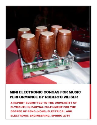
The Mini Congas were retrieved from Venezuela during Christmas 2013. A quick glance an
examination showed that the Mini Congas met the specifications as they were the right size, they
looked strong and sturdy and the heads were removable so the sensor could be placed. They also had
screw holes at the bottom to attach it to the box and an internal path to pass the wires through. Figure
39 shows the Mini Conga:
FIGURE 39: ONE MINI CONGA
50. 49
Figure 40 shows a Mini Conga with the lid open, where the sensor and the hole where its cables go
through can be appreciated:
FIGURE 40: MINI CONGA WITH LID LIFTED
51. 50
BOX ENCLOSURE AND STAND FOR SOLAR PANEL
The box enclosure was first designed by hand and then in AutoCAD. This was done in order to use an
automatic laser cutter instead of the manual drills and saws, making the final box more accurate and
clean. This job was done in the Faculty workshop at the bottom floor of Smeaton building. Figure 41
shows the AutoCAD model:
FIGURE 41: MECHANICAL DESIGN FOR BOX
52. 51
MECHANICAL ASSEMBLY
The assembly of the box was done using glue to join the polycarbonate together and it was left to dry
overnight. Also the hinges were screwed after the structure was solid. Figure 42 shows a photo of the
final product:
FIGURE 42: FINAL PRODCUT
53. 52
Figure 43 shows the solar panel attached to the stand and with the power cable soldered:
FIGURE 43: SOLAR PANEL WITH STAND
54. 53
MODIFICATIONS, IMPROVEMENTS, CHANGES & MISTAKES
The section before explained the design process without mentioning any challenges or problems
encountered. This section aims to explain the modifications done during the design stages in order to
get the final product to work. It also takes into account mistakes in the design and specifications that
could not be met.
Hardware
A series of modifications were made to the circuit because of wrongly placed components and
improvised improvements.
MODIFICATION #1
The first circuit alteration was done in the SPI lines interfacing the dsPIC with the SD card. This is
because the lines were originally wrongly connected; the SPI transmit line of the dsPIC was connected
to the SD card SPI transmit line and the same with the receive line. However the right configuration
would be to connect the transmit line to the receive line. The problem was fixed by lifting the 56 ohms
resistors and using a thin mod wire to connect it to the right line. Also the Chip Detect line from the SD
card was connected to a spare I/O pin. This was done so the program could detect the presence of a
card through hardware. Both modifications can be seen in Figure 44:
FIGURE 44: MODIFICATION 1
55. 54
MODIFICATION #2
When testing the analogue circuit it was noted that the trigger from the comparator where the reference
was 3.3V was not working. It was determined that this was because Vcc = Vref. No solution was
available as the schematic needed to be changed completely to add an extra voltage divider and its
respective tracks. For this reason, the gain function could not exist anymore as there will not be a way
to tell the dsPIC the amplitude of the signal.
MODIFICATION #3
The DAC external oscillator was not working initially. After debugging it, it was noticed that the pin
layout was wrong, pin 4 was were pin 6 should be and the other way around as it can be seen in Figure
45:
FIGURE 45: DUAL INVERTER WRONG LAYOUT
This was a very complicated issue to solve as the components used were extremely small and delicate.
It was decided to lift the legs of the IC and wire them with thin wire as seen in Figure 46:
FIGURE 46: MODIFICATION 3
56. 55
MODIFICATION #4
When programming the interrupts it was notice that not all the comparators were connected to external
interrupt capable pins. For this reason 3 tracks had to be re-routed using thin wire to usable pins. Pins
from the previous comparators that became unused after modification #2 were used as some of them
were already connected to external interrupt pins.
MODIFICATION #5
Some of the comparator triggers were working intermittently. It was determined that by removing the
Zener diodes used for protection the issue will go away. It was decide to completely remove all the
Zeners as the voltage should not go higher than Vcc after the buffer/amplifier, therefore they are not
required for protection.
MODIFICATION #6
When testing the PlaySample function, it was noticed that some sort of under buffering was happening
as it can be seen in Figure 46:
FIGURE 47: SIGNAL SUFFERING FROM BUFFER UNDERUN
It seemed that the program was not fast enough to catch up and some samples were being lost.
However after trying different solutions it was determined that the transfer speed between the SD card
and the dsPIC was not fast enough. In order to solve the issue the SPI transfer speed was increased to
its maximum, however the problem did not change. After more debugging it was found that the current
SD card used was Class 4 which has a transfer speed of 4.7MB/s, this was then upgraded to a Class
10 SD card with a speed of 14.6MB/s [34] which effectively fixed the issue.
57. 56
MODIFICATION #7
After upgrading the SD card the output from the DAC improved, however there were still intermittently
spikes happening as seen in Figure 48:
FIGURE 48: SIGNAL SUFFERING FROM SPORADIC SPIKES
It was determined that this was happening because of synchronization errors between the DAC and the
dsPIC as they were running off different clock sources. To solve this problem, the 16 MHz crystal was
removed and the track connecting the external oscillator to the dsPIC was enabled, making the whole
system run from a single clock. Software changes were made as appropriate. This modification fixed
the problem, further improving the output waveform of the DAC.
58. 57
MODIFICATION #8
When playing a low amplitude wave a noise could be heard. By probing the power supply it was
determined that this noise was caused by power supply ripple and it only happened while the DAC and
SD card were in use. The noise had a ripple at 390Hz, therefore perfectly audible, also it could reach
up to 80mV as seen in Figure 49:
FIGURE 49: VCC RIPPLE WHEN PLAYING A FILE
After debugging it was determined that the component causing the ripple was the SD card, Figure 50
shows the ripple only happening when the SPI CS line goes high (so SPI peripheral is in use):
FIGURE 50: RIPPLE HAPPENING AT THE SAME TIME AS SPI IN USE
59. 58
The first logical step to take was to increase the value of the decoupling capacitors in the SD card. This
was done, however it did not cause any changes. Then it was decided to increase decoupling in
general: larger capacitors were added in the voltage regulator and DAC, also smaller capacitors were
placed in parallel across the dsPIC decoupling capacitors in order to improve decoupling in general.
Again this did not produce any change. The final decision was to implement a low pass filter for the
power supply just before reaching the DAC Vcc pin. An LC filter with a corner frequency of 160 Hz was
decided to use with a 100uH inductor and a 10,000uF capacitor as it can be seen in Figure 51:
FIGURE 51: MODIFICATION 8
Luckily the capacitor fitted fine and the supply ripple was removed, solving the issue.
60. 59
MODIFICATION #9
The last circuit modification in this project is also concerned with audio quality. When listening to low
amplitude signal, a distortion that actually modulates the signal and makes it sound like something else,
happens. This issue has a massive impact in the audio quality making it very low, which is the opposite
of the required by the specifications. Figure 52 shows a low amplitude 1 KHZ sine wave and the effects
the distortion has on it:
FIGURE 52: SIGNAL SUFFERING FROM ALIASING
The signal has a slight staircase shape, therefore it was determined that the problem could be imaging.
For this reason a more sophisticated post-DAC LPF was implemented. It was decided to use the active
LPF that is recommended in the WM8727 DAC datasheet. However instead of using a non-inverting
amplifier configuration, an inverting amplifier was used, this is because even at the gain of 1, the
amplification will make the signal higher than Vcc, therefore going over the dynamic range the opamp
can support. Figure 53 shows the schematic of the filter:
FIGURE 53: ACTIVE LPF CIRCUIT
61. 60
Note that it is a stereo signal so two filters are required. Also the new filter was combined with the
previous RC filter.
Figure 54 shows the PCB layout of the active filter circuit:
FIGURE 54: ACTIVE LPF PCB LAYOUT
Figure 55 is a photo of the final PCB board with the components soldered:
FIGURE 55: ACTIVE LPF FINAL BOARD
62. 61
The new board was connected to the circuit, with the filtered power supply so the ripple will not affect
the signal. The new circuit was tested and it worked, however it did not remove the distortion. This
could only point that the error was in the DAC or file itself. It was then determined that the problem
came from an error in the program. The buffer reading the file in the SD card was set as a signed char
type. This was originally done because the data was 2’s compliment type. However in a signed char the
MSB will determine the sign, and lower will subtract from upper when the MSB is set. This means that
when reading the sample it was only reading half of the information, effectively down sampling it to 8-
bit. The data type was changed to “BYTE” and the issue was fixed.
Software
Because in software changing a parameter is easy and does not take all the complications of changing
a physical component in hardware, it only makes sense to talk about software modifications when the
main structure of the program is altered.
The only two cases where the main structured of software was altered was when it was decided to not
implement and program the gain adjustment function and the digital mixer.
The gain function was not implemented because of hardware issues as explained in modification #2.
On the other hand the reason to not implement the digital mixer function was because the product was
good enough as it was without the mixer and lack of time and ability to program it.
COSTS
The following are the costs involved in the project. All prices were checked in Farnell at the moment of
writing the report (10/04/2014).
Bill of Materials
ELECTRONIC COMPONENTS FOR CIRCUIT
Table 4 shows all the components used in the electronic circuit and the associated costs:
Category Quantity Value Unit Cost Total
Capacitors 4 4.7uF £0.037 £0.15
Capacitors 12 2.2nF £0.064 £0.77
Capacitors 24 100nF £0.064 £1.54
Capacitors 2 10uF £0.032 £0.06
Capacitors 3 10uF £0.037 £0.11
Capacitors 2 47nF £0.30 £0.60
Capacitors 2 26pF £0.064 £0.13
Capacitors 1 470nF £0.064 £0.06
Capacitors 2 15pF £0.064 £0.13
Resistors 7 1M £0.005 £0.04
Resistors 11 10K £0.005 £0.06
Resistors 6 1K £0.005 £0.03
Resistors 12 15K £0.005 £0.06
Resistors 1 430R £0.036 £0.04
64. 63
PCB
The PCB was sourced from an outside manufacturer, Table 6 compares different options:
Manufacturer Price Delivery included Turnover
PCB Pool £42 No Unknown
Quick-Tek £74 Yes 11 working days
PCB Train £43 Yes 15 working days
TABLE 6: COST OF DIFFERENT PCB MANUFACTURERS
PCB Train was selected as it offered a good price and acceptable delivery time. The PCB used for the
active filter board was produced in Smeaton and it cost £4.
SOLAR PANEL
The solar panel was selected from SelectSolar, an UK based company and it costed £25.00
MINI CONGAS
To workout the price of the Mini Congas it is a bit difficult as Venezuelan economy is very changeable.
Because the government has total control over foreign currency exchange, an alternative market called
“the black market” has developed where mainly $US can be bought at a high price. To compare, $1 at
the official rate is Bs.F 6.29 while the free market one $ is Bs.F 66.60. This is nearly 10 times more
expensive. Therefore when converting to another currency if the official rate is used it will seem as “too
expensive” or in the other hand if the black market rate is used it will seem as “quite cheap”. The
product cost was Bs.F 17,000. In Sterling Pounds that would be £1611, which is an insane amount, in
comparison it will be £152 when the black market rate is used. As most of the country uses the black
market rate because the government doesn’t give enough allowance to use foreign currency, the black
market price will be used as reference price for this project.
BOX ENCLOSURE
The components for the box were: the polycarbonate sheets with a cost of £4.98 and the hinges with a
cost of £1
MOD COMPONENTS
These are made from the components used for the power supply filter and the active filter. Table 7
shows the prices:
Category Quantity Value Unit Cost Total
Capacitors 2 1nF £0.064 £0.13
Capacitors 2 680pF £0.064 £0.13
Capacitors 4 10uF £0.064 £0.26
Capacitors 1 10,000uF £1.56 £1.56
Capacitors 1 100nF £0.064 £0.06
Resistors 2 1.8K £0.005 £0.01
Resistors 1 8.2K £0.005 £0.01
Resistors 2 10K £0.005 £0.01
Resistors 2 1K £0.005 £0.01
Resistors 2 47K £0.005 £0.01
Resistors 1 7.5K £0.005 £0.01
Resistors 2 169 £0.005 £0.01
65. 64
Inductors 1 100uH £0.115 £0.12
Integrated Circuits 1 MCP602 £0.42 £0.42
Total £2.73
TABLE 7: COST OF MOD COMPONENTS
TOTAL COST
Table 8 summarizes all costs and calculates the final cost of the project:
Item Cost
Electronic Components £20.33
Extra Components £24.02
PCB’s £47
Solar panel £25
Mini Congas £152
Box enclosure £5.98
Mod components £2.73
Total £277.06
TABLE 8: TOTAL COST OF PROJECT
The total cost of the project was £277.06. Note that the Mini Congas were privately funded while the
remainder £125.06 was used from the project budget.
TESTING
The following test were made to ensure the device was performing well and met the specifications
Battery Charging
This will test if the battery is successfully charged and how long it will take. The battery charger IC was
set to charge the battery at a constant current of 100mA, given that the battery capacity is of 550mAh
then theoretically the time it will take to charge the battery will be:
𝐶ℎ𝑎𝑟𝑔𝑖𝑛𝑔 𝑡𝑖𝑚𝑒 =
550𝑚𝐴ℎ
100𝑚𝐴
= 5.5 ℎ𝑜𝑢𝑟𝑠 𝑜𝑟 5 ℎ𝑜𝑢𝑟𝑠 𝑎𝑛𝑑 30 𝑚𝑖𝑛𝑢𝑡𝑒𝑠
USB
An USB cable was connected to the USB socket. The red LED turned on and it was left there until the
LED turned off, indicating that the charging process was complete.
SOLAR PANEL
The solar panel was first individually tested to measure the voltage and current when connected to the
load imposed by the charger. Using a multimeter the voltage was determined to be 4.1V after the
Schottky diode and the current 93mA. Then the same procedure used for the USB charging was
implemented giving the same results. Note that this only worked when the panel was exposed to bright
sunshine, this is because it was only at those levels of irradiance that the panel was able to produce the
required current.
66. 65
Power consumption and battery life
To determine power consumption, a multimeter measuring current was connected in series with the
ON/OFF switch terminals in order to measure the amount of current the device was using. It was
determined that when in idle the device will use 77.2mA, while in full use 123.6mA.
To determine battery life, an estimate must be calculated where the amount of current used in one hour
is the product of a combination of idle and full use mode.
In average a Salsa song has 100 Beats Per Minute (BPM), that means that each beat lasts 60/100 =
0.6 seconds. All dance genres are in 4/4, so one phrase will be 0.6 x 4 = 2.4 seconds, however the
Congas are normally played at the beat. Let’s say that in a 4 minute song the Congas are played for
60% of the duration of the song, that means that for 144 seconds (60x240/100) the Congas are used,
giving a total number of 60 hits per song (144/2.4), while 96 seconds (240 – 144) of idleness. In an hour
15 songs can be played (60/4). Then it is calculated that there is 36 minutes of full usage (15x144/60)
and 24 minutes of idleness (60-36). Then averaging the results to fit it a one hour format:
𝐶𝑢𝑟𝑟𝑒𝑛𝑡 𝑢𝑠𝑒𝑑 𝑖𝑛 𝑜𝑛𝑒 ℎ𝑜𝑢𝑟 =
(24𝑚𝑖𝑛 × 77.2𝑚𝐴) + (36𝑚𝑖𝑛 × 123.6𝑚𝐴)
60𝑚𝑖𝑛
= 105𝑚𝐴
This means that the total battery life in hours will be:
550𝑚𝐴ℎ
105𝑚𝐴
= 5.23 ℎ𝑜𝑢𝑟𝑠 𝑜𝑟 5 ℎ𝑜𝑢𝑟𝑠 𝑎𝑛𝑑 15 𝑚𝑖𝑛
This approximate number just fits the initial specification of 5 hours of battery life.
Delay
As explained in the software design section a debouncing method was used where the program will not
play any other sample for at least 10mS after the last sample. For this reason it can be inferred that the
total latency will be approximately 10mS as other processes do not have an important impact in the
total latency. This is well below the specifications which set minimum latency less than 100 mS.
Audio Quality
To asses audio quality there are many specific test that are normally used in the Hi-Fi industry such as
measuring the total harmonic distortion, signal to noise ratio, crossover and frequency response.
However to measure such parameters specialist equipment such as the Audio Precision analyzer are
required. Because of the lack of such equipment, the audio test will be a simple survey rating the audio
from 1 to 5 from 5 different users, the results are shown below in Table 9 (5 is the highest score):
User Score
User 1 5
User 2 3
User 3 5
User 4 3.5
User 5 4
Total score 4.1
TABLE 9: AUDIO QUALITY SCORE
67. 66
Debut night at the Havana Lounge
The device was tested in a “real world” environment by bringing it to an event and performing with it in
front of a crowd and with the intended equipment it was designed to be connected to. The event was
held in a local bar in Plymouth, the Havana Lounge, on Sunday the 20th
of April 2014. These are some
of the highlights from the experience:
The device connected successfully to the bar’s main mixer without introducing any ground loops
and with a good audio quality
Other artists/DJ’s/performers were impressed with the product
The size and weight of the device made it easy to carry and setup
The device did not need recharging for the period of use (approx. 3 hours)
The main drawback that was noted while using the device was that the device will trigger samples from
other sensors instead of the intended one. These means that it is hard to get a coherent pattern while
playing, since it is unpredictable when the device will play the right sample. Figure 56 shows the device
connected to the main mixer:
FIGURE 56: DEVICE CONNECTED TO THE BAR’S MAIN MIXER
68. 67
DEVICE USER MANUAL
This is a quick start guide for the user that desires to start using the Mini Electronic Congas
Strokes legend:
1: Touch 3: Bass 5: Muffle
2: Slap 4: Open 6: Open Slap
Refer to Figure 57 in the next page.
How to play
A video tutorial can be downloaded here
How to change samples
Please follow the step by step guide:
1. Download and install the Open Source audio editor Audacity.
2. Open Audacity and load your file
3. Make sure the Project rate is set at 48000 Hz, this can be changed at the bottom left corner
4. Make sure there are no peaks in the file, this can be seen by clicking View>Show Clipping
5. If red lines appear it means there is clipping and needs to be removed
6. To remove clipping, select all the file and click Effect>Normalize
7. In the amplitude parameter type in: -0.1 and click OK
8. The file is ready now to be exported, click File>Export
9. In the Save as type box select: Other uncompressed files and then click the Options box at the
bottom right of the new window
10. In header select: RAW (header-less) and in Encoding select: Signed 16 bit PCM
11. Click OK to close the options and then save to save the file
12. Save the file to the SD card under the name Sample_X where X can be any number from 1 to 6
13. Figure 56 shows the corresponding sample number to Mini Conga location:
69. 68
FIGURE 57: MINI CONGAS TO SAMPLE NUMBER REFERENCE
Things not to do
Please do not attempt to do any of the following as its consequences are unknown and might
negatively affect the product:
Do not connect the solar panel and USB power at the same time
If files are loaded that have clipping this will be heard in the audio playback as clicks and pops
Loading a file with a different sampling rate will play the file at a different speed and pitch
Hitting the Mini Congas too hard will spread the vibrations across the board, triggering other
Mini Congas
CONCLUSIONS
This is the final section of the report. It will go through recommendations for the next version and a final
wrap up.
Future Improvements & Recommendations
This is a list of different modifications that can be done to the final product to increase its quality and
also to mass produce it.
HARDWARE
The first changes to the circuit should be to apply the modifications described in the previous section to
the PCB board, this involves:
Re-tracking of wrongly placed lines such as the SPI and the external interrupts
Fix wrong PCB packages such as the one used for the dual inverter
Add an extra voltage divider to setup a new reference for the comparators
Remove Zener diodes used in the buffer/amp stage
Remove the 16 MHz crystal and the passive components used for its circuit
Increase general decoupling, in particular near the SD card
1
2
3
4
5
6
SD
70. 69
Include the active filter circuit in the main PCB
Extra hardware modifications
These are other modifications that were not implemented but can improve the final product
General
Add a voltage divider before the buffer/amp to attenuate the signal from the piezoelectric
sensor. This is required because the signal coming from the sensors is higher than 3.3V and it
gets even more amplified by the non-inverting amplification factor of 2. This makes mostly all
taps to the drums to produce a signal in saturation, therefore triggering the comparator. This is
unwanted as it is harder to distinguish a strong tap from a soft tap. Another solution is get
different sensors that produce a smaller voltage. By properly distinguishing the signals it might
be possible to remove the TMR1 10 mS debouncing implementation, reducing the total latency
considerably
The current circuit features two different connections for the debugger, this was for precaution
as the designer was not sure about which connection was the right one. One of them can be
taken away now as the right connection is now known.
Also shortening some ground tracks and connections will be beneficial
Another desired connector to add to the board will be a mini jack output, making the device able
to connect to other devices using different types of cables
Power saving
Further reading into the DAC datasheet shows that the device can be turned off if the MCLK
signal is removed, therefore saving a substantial amount of power. This can be done by using a
simple BJT switch configuration controlled be a GPIO pin in the dsPIC.
SOFTWARE
As the software was left incomplete, it will be desirable for the next version to successfully implement
the gain adjustment feature and the digital mixer. Apart from that a few modifications can be made by
an experienced programmer:
Use of Direct Memory Access (DMA) to send the samples to the DAC through the DCI
peripheral: the DCI peripheral is capable of use DMA: by reading the samples directly from
memory instead of waiting for the CPU to fetch them can increase the performance, therefore
reducing the latency. However it might not be necessary for this application as the latency is
already kept in low values
DSP implementation: the special DSP functions were never used as no mathematical
operations were implemented. In the case of implementing the gain adjustment and digital
mixer, the DSP functions could be beneficial as it will increase the speed of the process.
However, again, it might not be necessary for this application.
UNKNOWN ISSUES
There was only one issue in this project that negatively affected the final product considerably. It was
regarding audio quality and was addressed with modification 8.
The supply ripple from modification 8 was fixed by inserting a high value capacitor, however this is not
a practical solution for the application because of its big size and relatively high cost. For this reason,
71. 70
this problem should be addressed differently in the next version. It is known that is caused by the
current used by the SD card however it seems uncommon to be a normal issue as there are many
devices that use SD cards to play audio files and are powered by a 3.7V Li-Ion battery such as mobile
phones for example. Attempts were made to solve this issue by changing the values of the pull-up
resistors in the SPI line and changing the speed of the SPI clock. Also as mentioned before, bypass
and decoupling capacitors were added but it did not change the problem. The board was even directly
connected to an external power supply to see if the problem was the battery or the regulator, however,
again, it did not change.
COST REDUCTIONS
It is possible to reduce the cost of the final product by changing components for cheaper ones and not
using some.
Electronic components
Referring to the cost tables before it can be seen that the most expensive components were the DAC
and the dsPIC. A cheaper MCU could easily be chosen if it’s determined that the 40 MIPS CPU speed
and DSP functions are not required.
Other components
It is obvious that the solar panel was not necessary. This was more of a proof of concept and a
philosophical decision for the project, so the device is completely stand-alone and capable of
recharging its own battery using renewable energy. Therefore if this is mass produced, the solar panel
can be discarded straight away or offered as an accessory.
The other very expensive component was the Mini Congas. As this was produced by an instrument
maker, strictly following the design guidelines, the price paid for the product was the same one will pay
an artist for a piece of art. This will not be the case if mass produced, since the process can be
automated in a factory, producing thousands of parts, reducing the price tremendously.
Final Thoughts
This project has been a very complete work where the electronic circuit, software and product design
were all evaluated and designed in order to produce a final product. In industry this is normally done by
separate engineering departments.
Furthermore the product was tested in real usage conditions to evaluate its performance in the variable
and unpredictable conditions of real life.
The result was a fully working device that can be used as initially intended, to improvise as a drummer
during long periods of waiting and to increase the “performance” factor of the DJ.
Finally I would like to add that this has been a great experience were I have combined the knowledge
acquired in my degree with the practical experience I got in my placement year with Cambridge Audio
to produce a tangible and useful device that works and entertains. For me this is what engineering is,
using science to produce devices that improve human existence in some way. In this case, is giving
anyone the possibility to become a Latin Conga drummer with less effort compared to the traditional
way, as no technique is required, only rhythm and a bit of memory. (This last paragraph was written in
first person deliberately).